ABSTRACT
LI, CHAO. Optimizing Memory Efficiency for Many-Core Architecture. (Under the direction of Dr. Huiyang Zhou).
Massively parallel, throughput-oriented processors such as graphics processing units (GPUs) leverage high thread-level parallelism to overlap long latency memory accesses with computation. On-chip memory resources, including register files, shared memory, and data caches which were designed to provide high-bandwidth low-latency data accesses, remain critical to application performance.
In this dissertation, we study these memory resources and propose optimizations to improve the memory efficiency for GPU architecture in a whole stack, from hardware architecture, compiler, to application-level algorithms. First, I will present our work on understanding the tradeoffs between software-managed vs. hardware-managed caches in GPUs. To manage on-chip caches, either software-managed or hardware-managed schemes can be employed. State-of-the-art accelerators, such as the NVIDIA Fermi or Kepler GPUs support both software-managed caches, aka. shared memory, and hardware-managed L1 data caches (D-caches). Shared memory and the L1 D-cache on a GPU utilize the same physical storage and their capacity can be configured at runtime. In this work, we present an in-depth study to reveal interesting and sometimes unexpected tradeoffs between shared memory and the hardware-managed L1 D-caches in GPU architecture.
Secondly, I will present our novel compiler scheme for the judicious utilization of on-chip memory resources on GPUs. To manage these intricate on-on-chip memory resources is non-trivial for application developers. Moreover, the varying on-chip resource across different GPU generations makes performance portability a daunting challenge. In this study, we propose compiler-driven automatic data placement scheme, to refine GPU programs by altering data placement among different on-chip resources to achieve both performance enhancement and performance portability.
On-contain a significant amount of requests with low reuse, which greatly reduce the cache efficacy. We propose an efficient locality monitoring mechanism to dynamically filter the access stream on cache insertion such that only the data with high reuse and short reuse distances are stored in the L1 D-cache. We propose a design that integrates the locality filtering functionality into the decoupled tag store of the current L1 D-cache through simple and cost-effective hardware extensions.
© Copyright 2016 Chao Li
Optimizing Memory Efficiency For Many-Core Architecture
by Chao Li
A dissertation submitted to the Graduate Faculty of North Carolina State University
in partial fulfillment of the requirements for the degree of
Doctor of Philosophy
Computer Engineering
Raleigh, North Carolina
2016
APPROVED BY:
_______________________________ _______________________________
Huiyang Zhou Gregory Byrd Committee Chair
_______________________________ _______________________________
DEDICATION
BIOGRAPHY
Chao Li was born in Lianyungang, a beautiful city in the northeastern Jiangsu province in China. He received his bachelor degree on software engineering from DaLian University of Technology(DLUT) in 2009 and got his master degree in computer science and technology from Institute of Software, Chinese Academy of Sciences (ISCAS) in 2012.
ACKNOWLEDGMENTS
I would like to express my greatest gratitude for those who have helped me through my PhD period. First and foremost, I would like to thank my PhD advisor, Dr. Huiyang Zhou. Without his support and guidance, this dissertation would not have been possible. I would like to express my greatest gratitude to him for the tremendous time, effort and wisdom that he has invested in my graduate research. His insightfulness on research and responsible attitude towards life will be treasured by me for a long time.
I also would like to thank Dr. James Tuck, Dr. Xipeng Shen and Dr. Gregory Byrd for serving on my PhD advisory committee. I would like to show my appreciation to Dr. Yi Yang, Dr. Frank Mueller, Dr. Shuaiwen Song and Dr. Shengen Yan, Dr. Albert Sidelnik, Dr. Siva Hari, Michael Mantor for their great suggestions and collaborations on my research.
Many thanks go to my colleagues including Hongwen Dai, Xiangyang Guo, Qi Jia, Zhen Lin, Yuan Liu, Yi Yang, Ping Xiang and Saraubh Gupta for their helps during my study. I especially want to thank Yi Yang and Hongwen Dai for their valuable advices in my research. Also, I would like to express my thanks to Amro Awad and Sungkwan Ku for their friendship and generous help.
I would like to thank my wife Jing Rao, my father Dayong Li, my mother Xiuju Zhang, my brothers Jiling Li, Yuling Li so deeply for their continuous support, trust and love.
TABLE OF CONTENTS
LIST OF TABLES --- viii
LIST OF FIGURES --- ix
Chapter 1 ... 1
1 Introduction ... 1
Chapter 2 ... 4
2 Understanding the Tradeoffs between Software-Managed vs. Hardware-Managed Caches in GPUs ... 4
2.1 Introduction ... 4
2.2 Background ... 6
2.3Tradeoffs between shared memory and L1 D-caches ... 7
2.3.1 Case Study I: Matrix Multiplication ... 7
2.3.2 Case Study II: Fast Fourier Transform (FFT) ... 13
2.3.3 Case Study III: Matching Cube (MC) ... 17
2.3.4 Case Study IV: Path Finder (PF) ... 19
2.4 Experiments ... 21
2.4.1 Experimental Methodology ... 21
2.4.2 Experimental Results on GTX 480 and GTX680 GPUs ... 23
2.4.3 Experimental Results on GPGPUsim ... 24
2.4.4 The TLP Impact of the D-Cache Versions ... 27
2.4.5 Impact on Energy Consumption ... 28
2.4.6 Summary ... 30
2.5 Related Works. ... 30
2.6 Conclusions ... 31
Chapter 3 ... 32
3 Automatic Data Placement into GPU On-Chip Memory Resources ... 32
3.1 Introduction ... 32
3.2 Background and Motivation ... 34
3.3.1 Data Placement Patterns ... 37
3.3.2 Compiler Algorithms and Implementation ... 45
3.4 Experimental Methodology ... 51
3.5 Experimental Results ... 52
3.6 Related works... 58
3.7 Conclusion ... 59
Chapter 4 ... 61
4 Locality-Driven Dynamic GPU Cache Bypassing ... 61
4.1 Introduction ... 61
4.2 Background ... 63
4.2.1 Baseline Architecture ... 63
4.2.2 Baseline Memory Request Handling ... 64
4.3 GPU Cache Inefficency and Workload Analysis... 66
4.3.1 GPU Cache Inefficiency ... 67
4.3.2 Impact of Applications On Performance ... 70
4.4 Design Methodology ... 72
4.4.1 Decoupled L1D: Structure ... 74
4.4.2 Decoupled L1D: Operations ... 75
4.4.3 SM Dueling ... 76
4.5 Experimental Methodology ... 77
4.6 Result And Analysis ... 78
4.6.1 Overall Performance Evaluation ... 78
4.6.2 Design Space Exploration ... 87
4.6.3 Sensitivity to L1 D-cache Sizes ... 90
4.6.4 Sensitivity to Warp Scheduling Policies ... 91
4.6.5 Hardware Cost And Energy Efficiency ... 92
4.7. Ralted Work ... 92
4.8. Conclusions ... 94
Chapter 5 ... 95
5 Optimizing Memory Efficiency for Deep Convolutional Networks on GPUs ... 95
5.1 Introduction ... 95
5.2.1 Convolutional Neural Networks ... 98
5.2.2 Deep CNN Libraries ... 101
5.3 Methodology ... 101
5.4 Memory Issue A: Data Layout ... 103
5.4.1 Data Layout in Convolutional Layers ... 103
5.4.2 Data Layout in Pooling Layers ... 109
5.4.3 A Fast Data Layout Transformation for CNNs... 110
5.4.4 Wrap Up: Automatic CNN Data Layout Support ... 112
5.5 Memory Issue B: Off-chip Memory Accesses ... 113
5.5.1 Memory Analysis and Optimization on Pooling Layers... 113
5.5.2 Memory Analysis and Optimization on Softmax Layers ... 114
5.6 Results and Analysis ... 117
5.6.1 Results on Data Layout Optimization ... 117
5.6.2 Results on Off-chip Memory Access Optimization ... 120
5.6.3 Results on Whole Networks... 121
5.7 Related Works ... 124
5.8 Conclusion ... 126
Chapter 6 ... 127
6 Instruction Cache Study for GPU Architecture ... 127
6.1 Introduction ... 127
6.2 Background ... 128
6.3 Methodology ... 129
6.4 GPU Instruction Cache Efficiency Analysis... 131
6.5 Memory Prefetcher ... 134
6.6 Experimental Results ... 134
6.7 Summary ... 136
Chapter 7 ... 137
7 Conclusion ... 137
LIST OF TABLES
Table 2.1. The GPGPUsim configuration. ... 21
Table 2.2. The benchmarks used in experiments. ... 22
Table 3.3. A comparison of hardware characteristics across different GPU generations. ... 36
Table 3.2. Parameters used in experiments. ... 51
Table 3.3. Benchmarks and their resource usage. ... 52
Table 3.4. The auto-tuning time on GTX 680 ... 56
Table 4.1. Application categorization based on cache bypassing impact. CNF: Cache Unfriendly, CI: Cache Insensitive, CF: Cache Friendly. IPC is normalized to the case of all taking L1 D-Path (N-IPC). The selected applications include Particular Filter (PTF), Srad2 (SD2), Needleman-Wunsch (NW), Single-Source Shortest Path (SSSP), LU Decomposition (LUD), Hotspot (HS), Barnes-Hut (BH), CFD Solver (CFD), Leukocyte (LFK), Gaussian Elimination (GS), Fourier Transformation (FFT), Myocyte (MYC), PathFinder (PF), Srad1 (SD1), Heartwall (HT), Matrix Multiplication (MM), B+Tree (BT), and Back Propagation (BP). ... 66
Table 4.2. Baseline architecture configuration. ... 77
Table 4.3. Configurations of our proposed Decoupled L1D. ... 78
Table 5.1. The CNNs and their layers used in the experiments. ... 101
Table 6.1. Baseline Architecture Configurations. ... 130
LIST OF FIGURES
Figure 3.6. The compiler algorithm to promote shared or global memory to registers to be shared among threads. ... 48 Figure 3.7. Performance speedups achieved by automatic data placement for all benchmarks on three different GPUs. ... 53 Figure 3.8. Auto-tuning of our automatic data-placement for all benchmarks on GTX680 (Performance normalized to original kernel). ... 54 Figure 3.9. The optimal parameter, the number of shared memory array to be promoted and the C-Factor, determined for different GPUs. ... 55 Figure 3.10. Performance speedup of optimized kernels in Marching Cubes with different input sizes... 57 Figure 4.1. Memory request handling in the baseline architecture. ... 64 Figure 4.2. L1 (right) and L2 (left) level contention study by increasing their associativity and capacity. It clearly shows that the major performance bottleneck resides at the L1 D-cache level for CNF workloads... 68 Figure 4.3. Reuse breakdown for CNF applications. It shows the percentage of addresses in L1 D-cache have been referenced by m number of times. The values of m are shown in the legend. ... 70 Figure 4.4. The reuse distance histograms of L1 D-cache access stream of the CNF
Figure 5.1. Performance comparison between the CHWN layout (cuda-convnet2) and
NCHW layout (cuDNNv4) on convolutional and pooling layers in AlexNet [72] ... 96 Figure 5.2. The structure of an example CNN. ... 99 Figure 5.3. Performance comparison between two different data layouts for the convolutional layers in Table 5.1. The performance is normalized to cuda-convnet measured on GTX TITAN BLACK. ... 105 Figure 5.4. Sensitivity study of data layouts on the N and C dimensions. CONV7 in Table 5.1 is used while others show similar trends... 106 Figure 5.6. Performance comparison between different data layouts for the pooling layers in Table 5.1. The performance is normalized to cuda-convnet. The numbers on top denote the highest bandwidth (GB/S) achieved for each layer. ... 110 Figure. 5.7. Kernels for data layout transformation implementation ... 111 Figure 5.8. Overlapped pooling with a window size of 4. The 2D image is simplified to 1D. vector... 113 Figure 5.9. Optimized kernel after kernel fusion(C<11K) ... 116 Figure 5.10. Speedups achieved on all convolutional layers. For both NCHW and CHWN data layout, the best achieved performance is measured on calculating the performance difference. ... 118 Figure 5.11. Achieved memory bandwidth using three methods for data layout
transformation. The Transform-Opt2 is not available for CV10, CV11, CV12 whose N is smaller than 64. ... 119 Figure 5.12. Performance comparison among four different implementations for the pooling layers in Table 5.1. The performance is normalized to cuda-convnet. ... 120 Figure 5.13. Performance comparison (GB/S) of softmax layers with a wide range of
configurations. x/y means the batch size x and the number of categories y. ... 121 Figure 5.14. The overall network performance comparison among various schemes. ... 123 Figure 5.15. The performance comparison of different layers in AlexNet, Time Speedup Normalized to cuDNN-MM. “Opt_NoTran” bar denotes the performance without the
Chapter 1
Introduction
developers to explicitly manage shared memory with the existence of the hardware managed L1 D-caches in GPUs? And (b) what are the main reasons for code utilizing shared memory to outperform code leveraging L1 D-caches (and vice versa)? To answer them, we present an in-depth study to reveal interesting and sometimes unexpected tradeoffs between shared memory and the hardware-managed L1 D- caches in GPU architecture.
Secondly, as observed in our first work, the trade-offs among these on-chip memory resources are complex and sometimes non-intuitive. Thus, it is non-trivial for application developers to explicitly manage these on-chip memory resources for high memory efficiency. More importantly, as on-chip resources have been changing significantly for different generations of GPUs, an optimized kernel upon one generation becomes suboptimal on another one. Thus performance portability becomes a daunting challenge for application developers. We tackle this problem with compiler-driven automatic data placement. We focus on programs that have already been reasonably optimized either manually by programmers or automatically by compiler tools. Our proposed compiler algorithms refine these programs by revising data placement across different types of GPU on-chip resources to achieve both performance enhancement and performance portability.
Chapter 2
Understanding the Tradeoffs between
Software-Managed vs. Hardware-Software-Managed Caches in
GPUs
2.1 Introduction
To manage on-chip caches effectively, either explicit software management or implicit hardware management schemes have been widely used in computer systems. While hardware-managed caches relieve the application developers of explicit data management, it is expected that software approaches may offer higher cache performance (i.e., hit rates) with the knowledge of data reuse patterns. State-of-art graphics processing units (GPUs), such as the NVIDIA GTX480 and GTX680 GPUs, include both software managed caches, aka. shared memory, and hardware managed L1 data caches (D-caches). An outstanding feature of these GPUs is that shared memory and L1 D-caches utilize the same physical resource and their capacities can be configured through APIs. As a result, GPUs provide an ideal platform to study the intriguing tradeoffs between hardware-managed caches and software-managed caches.
managed L1 D-caches in GPUs? And (b) what are the main reasons for code utilizing shared memory to outperform code leveraging L1 D-caches (and vice versa)?
We start our journey with the well-known matrix multiplication algorithm. From an optimized kernel using shared memory, we remove shared memory arrays while ensuring that the same tiling optimization has been applied. As the tiles fit in the D-cache/shared memory capacity, both versions enjoy very high hit rates after the tiles are initially loaded into shared memory/the L1 D-cache. The measured execution times on GTX480 GPUs (GTX680 GPUs do not cache global memory data in L1 D-caches), however, show that the L1 D-cache version is surprisingly much slower (43.8%) than the shared-memory version. Puzzled with these results, we resort to a GPU architectural timing simulator, which reports a similar performance trend, to retrieve detailed execution statistics. Through micro-kernels, assembly-level code analysis, and cycle-by-cycle instruction execution information, we pinpoint the unexpected reason: the shared-memory version achieves much higher memory-level parallelism (MLP) than the L1 D-cache version. Other factors including hit rates, memory coalescing, and dynamic instruction counts, have relatively little impact in comparison.
Besides matrix multiplication, we also perform detailed case studies on FFT, MC, and PF due to their distinctive data access patterns. Then, we categorize a set of 16 GPGPU workloads based on whether or not there is data sharing among threads. Our results show that for most applications, the GPU kernels utilizing shared memory deliver significantly higher performance than those leveraging L1 D-caches. The fundamental reasons are MLP and coalescing. For a few benchmarks for which the L1 D-cache versions have higher performance, the performance impact is mainly due to improved thread-level parallelism (TLP) and allocating more data to registers. Overall, rather than cache hit rates, the subtle factors including MLP, coalescing, and TLP often have more profound performance impacts.
and discusses their tradeoffs in utilizing shared memory or L1 D-caches. Section 2.5 addresses the related work. Section 2.6 concludes the chapter.
2.2 Background
State-of-art GPUs leverage high degrees of TLP to achieve high computational throughput. In GPU programming models such as NVIDIA CUDA [6], a GPU kernel is launched as a grid of thread blocks (TBs) and each TB in turn contains many threads. During execution, the threads in a TB are grouped into multiple warps based on their thread identifiers (ids) and threads in a warp execute in a lockstep manner, meaning that there is one program counter (pc) for all the threads in a warp.
shared-memory usage is that it may limit the number of TBs that can run concurrently in an SM.
2.3
Tradeoffs between shared memory and L1 D-caches
2.3.1 Case Study I: Matrix Multiplication
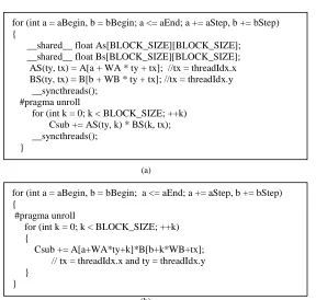
For matrix multiplication with large matrices, the key optimization is loop tiling/blocking to reduce the working set size and thereby reduce reuse distances. The matrix multiplication kernel from CUDA SDK [5] uses shared memory to store the tiles and the code is shown in Figure 2.1a.
The code in Figure 2.1a computes a tile of elements in the product matrix. It reads a tile from either of the two input matrices and stores the two tiles into shared memory. Then, it performs multiplication between the two tiles before moving on to the next set of tiles. Since the tiles already reside in shared memory when multiplication is performed, the accesses to the tiles have low latency, thereby achieving high performance. This code illustrates the explicit way of managing data, which dictates where the data are stored and where to access them. It also showcases an overhead of shared-memory usage. The data are loaded to registers first and stored to shared memory. The same data will then be loaded again from shared memory into registers to perform computation. Such redundant data accesses result in increased dynamic instruction counts.
capacity as 48kB on a GTX480 GPU. For the D-cache version, we configure the L1 D-cache capacity as 48kB on the same GPU. The input matrices have a size of 256x256 and the tile size is 16x16. Therefore, each tile has a size of 1kB (=16x16x4B). With either configuration, the register usage is the limiting factor on how many TBs can run concurrently on an SM. For both versions, 5 TBs can run concurrently on a TB. Since the L1 D-cache and shared memory actually use the same physical on-chip storage and the capacity is large enough for the working sets (10kB for 5TBs), our initial expectation is the two versions should have similar performance. If we consider the instruction overhead for explicit data movement, the shared-memory version may have a slightly lower performance. Our actual experimental results on the GTX480 GPU, however, show that the D-cache version, (i.e., the code in Figure 2.1b) is 43.8% slower than the shared-memory version (i.e., the code in Figure 2.1a).
To explain the unexpected experimental results, we first use a micro-benchmark, similar to the one used in [16], to measure the shared-memory access latency and the L1 D-cache hit latency. Our experimental results show that for GTX480, the shared-memory access latency is 44 cycles and the L1 D-cache hit latency is 80 cycles. However, considering the fact that the benchmark matrix multiplication has a high degree of TLP to hide such latencies, the latency difference may not be a reason for our observed performance difference. Also, it is not clear how much the data movement overhead costs on the actual hardware. Therefore, we resort to a microarchitectural-level timing simulator, GPGPUsim V3.2.1 [2], to simulate the two code versions on a GPU configuration similar to GTX480. The shared-memory access latency and the L1 D-cache hit latency are 3 cycles and 1 cycle, respectively, in this simulator shared memory and the L1 D-cache both have the same throughput of 1 access per cycle. The results from the simulator show a trend similar to our actual hardware measurements, i.e., the D-cache version is 112.2% slower than the shared-memory version.
shared-memory version but offers no explanation why the shared-shared-memory version has much higher performance.
Figure 2.1 Code segments for the matrix multiplication kernel. (a) The kernel explicitly uses shared memory to store tiles (i.e., the shared-memory version); (b) the kernel implicitly uses the L1 D-cache to store tiles (i.e., the D-cache version).
Suspecting that the D-cache may suffer from conflict misses since the capacity is sufficient for the working sets, we use a perfect cache without any misses. Our results show that even with a perfect cache, the shared-memory version is still 0.2% faster than the D-cache version. Puzzled with the results, we craft a microkernel to check whether it is possible for a D-cache version to outperform its equivalent shared-memory version. This microkernel loads a block of data and then re-accesses the same block many times. The results from this micro-benchmark confirm that the D-cache version is 13.0% faster than the corresponding shared-memory version (i.e., the block of data is located in shared shared-memory). The data movement in the shared-memory version accounts for 8.3% dynamic instruction count overhead in this
for (int a = aBegin, b = bBegin; a <= aEnd; a += aStep, b += bStep) {
__shared__ float As[BLOCK_SIZE][BLOCK_SIZE]; __shared__ float Bs[BLOCK_SIZE][BLOCK_SIZE]; AS(ty, tx) = A[a + WA * ty + tx]; //tx = threadIdx.x BS(ty, tx) = B[b + WB * ty + tx]; //tx = threadIdx.y __syncthreads();
#pragma unroll
for (int k = 0; k < BLOCK_SIZE; ++k) Csub += AS(ty, k) * BS(k, tx); __syncthreads();
}
for (int a = aBegin, b = bBegin; a <= aEnd; a += aStep, b += bStep) {
#pragma unroll
for (int k = 0; k < BLOCK_SIZE; ++k) {
Csub += A[a+WA*ty+k]*B[b+k*WB+tx]; // tx = threadIdx.x and ty = threadIdx.y }
}
(a)
microkernel. With this result, now we are facing two key questions for the matrix multiplication kernel: (a) Why is the D-cache version slightly slower than the shared-memory version even with a perfect cache? (b) With a realistic cache, why is the D-cache version much slower?
To answer the first question, we look into the cycle-by-cycle instruction execution through the GPU pipeline. We observe that the load instruction corresponding to the array access ‘A[a+WA*ty+k]’ in Figure 2.1b experiences additional pipeline stalls. The reason is that for a warp of 32 threads, when the TB dimension is 16x16, will have two rows of threads. For example, threads in warp 0 in TB 0 will have the thread id along the X direction, threadIdx.x, ranging from 0 to 15 and the thread id along the Y direction, threadIdx.y (i.e., ty in A[a+WA*ty+k]), ranging from 0 to 1. As a result, for this warp, the load instruction will access A[a+WA*0+k] and A[a+WA*1+k]. With a cache-line size of 128 bytes, these two accesses will fall into two separate cache lines. In other words, two cache accesses are needed to complete this load instruction for each warp using the D-cache version. In contrast, for the shared-memory version, the tiles are stored into shared memory before the loop. Then, inside the loop, the array access ‘AS(ty,k)’ will correspond to AS(0,k) and AS(1,k) for warp 0. With shared memory featuring 32 banks and the dimension of the array AS of 16x16, both the elements AS(0,k) (i.e., AS[k]) and AS(1,k) (i.e., AS[1x16+k]) are located in the same row with k ranging from 0 to 16. Therefore, one shared memory access completes the shared-memory load instruction corresponding to ‘AS(ty,k)’. Since the array access ‘A[a+WA*ty+k]’ of the D-cache version cannot be coalesced into a single cache access, it suffers from additional pipeline stalls even though all accesses hit in cache. Such overhead overweighs the benefit of fewer instruction counts compared to the shared-memory version, thereby resulting in lower performance even with a perfect cache.
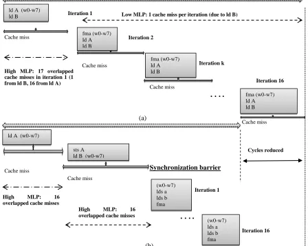
16kB to 48kB but the miss rate does not vary significantly. This is reasonable as the working set of an SM, i.e., 5TBs, is just 10kB. Therefore, considering the large performance gap, cache misses should not be the key culprit of the poor performance of the D-cache version. Again, we resort to cycle-by-cycle instruction-level analysis to understand what happens at run-time. We found that performance is not determined by the total number of cache misses. Instead it depends more on how these cache-misses overlap with each other, i.e., the degrees of memory-level parallelism (MLP).
ld A (w0-w7)
ld B Iteration 1
fma (w0-w7) ld A ld B Iteration 2 Cache miss fma (w0-w7) ld A ld B fma (w0-w7) ld A ld B Iteration k
….
Cache miss Cache miss Cache missLow MLP: 1 cache miss per iteration (due to ld B)
ld A (w0-w7)
sts A ld B (w0-w7)
(w0-w7) lds a lds b fma (w0-w7) lds a lds b fma Synchronization barrier
….
Iteration 16 Iteration 1 Iteration 16 High MLP: 16overlapped cache misses Cache miss
Cache miss
Cycles reduced Each inner llop (a)
(b)
Figure 1.2. Memory-level parallelism of the matrix multiplication kernel. (a) The D-cache version, (b) the shared-memory version.
High MLP: 17 overlapped cache misses in iteration 1 (1 from ld B, 16 from ld A)
With the D-cache version, for each warp, during each iteration of the inner loop ‘for (int k = 0; k < BLOCK_SIZE; ++k)’, the access to array B ‘B[b+k*WB+tx]’ is a cache miss (e.g., tx = 0~15 for warp 0, warp 1, etc.) due to the large value of ‘WB’. In other words, for each different k, the access ‘B[b+k*WB+tx]’ is a cache miss. The access to array A ‘A[a+WA*ty+k]’ results in two misses (e.g., ty=0~1 for warp 0, ty = 2~3 for warp 1, etc.) for the first iteration (i.e., k=0) and hits in the cache for subsequent iterations. These two loads are followed by a dependent floating-point multiply-and-add (fma) instruction. Therefore, the cache misses are distributed across iterations. Considering a TB with a round-robin warp scheduling policy, the warps make similar progress and different warps can also overlap their misses, as shown in Figure 2.2a. However, as the access to array B ‘B[b+k*WB+tx]’ has an index independent on the thread id along the Y direction, with a TB size of 16x16, all warps in a TB will access the same address during the kth loop iteration. In other words, the misses due to accessing array B remain distributed across loop iterations. In comparison, for the shared-memory version, the code before the inner loop forces the tiles to be loaded from global memory and stored in shared memory before computation. For array B, the access ‘B[b+WB*ty+tx]’ ensures that the entire tile from array B will be loaded by different warps: warp 0 accesses ‘B[b+WB*ty+tx]’ with tx=0~15 and ty=0~1; warp 1 accesses ‘B[b+WB*ty+tx]’ with tx=0~15 and ty=2~3, etc. Therefore, all the cache misses from different warps in a TB are aggregated and overlapped with each other, as shown in Figure 2.2b. Comparing Figure 2.2a with Figure 2.2b, we can see that much higher MLP is achieved with the shared-memory version. Therefore, with a realistic cache, the performance of shared memory is much better than the D-cache version although both versions have similar numbers of total cache misses.
Figure 2.3. The D-cache version of matrix multiplication with prefetching instructions to improve MLP.
In summary, for matrix multiplication, the two key reasons for its shared-memory version to outperform the D-cache version are (a) its high MLP as the tiles are loaded into shared memory before computation; and (b) shared memory has 32 banks and is much less susceptible to the coalescing problem compared to the D-cache. In comparison, the classical metric of cache performance, i.e., the cache-miss/hit rate, is less critical than these two factors.
2.3.2 Case Study II: Fast Fourier Transform (FFT)
In this case study, we use a radix-4 based 1-D FFT kernel. The test input is a 1k-point FFT with a batch size of 4k. For a 1k-point FFT, each thread goes through multiple stages with each stage performing a 4-point FFT and then exchanging data with other threads. As a result, the key to achieve high throughput is to hold all the intermediate results in shared memory or the D-cache. The sample code of the radix-4 based FFT using shared memory and the D-cache is shown in Figure 2.4. Comparing the two versions, we can see that they are identical except that one uses a shared-memory array to keep the intermediate results and the other uses a global-memory array to do so. If the cache is large enough to keep the temporary data, all the accesses will be cache hits and enjoy low access latency.
For the two FFT kernels, we first test them on a GTX480 GPU. For the shared-memory version, the shared-memory capacity (48kB) limits the number of concurrent TBs on an SM to
for (int a = aBegin, b = bBegin; a <= aEnd; a += aStep, b += bStep) {
prefetch(A[a + WA * ty + tx]); //Prefetch the tile of matrix A prefetch(B[b + WB * ty + tx]); //Prefetch the tile of matrix B __syncthreads();
#pragma unroll
for (int k = 0; k < BLOCK_SIZE; ++k) {
Csub += A[a+WA*ty+k]*B[b+k*WB+tx]; // tx = threadIdx.x and ty = threadIdx.y }
be 5. For fair comparison, we also apply the same limit to the D-cache version with an unused share-memory array in the code. We also vary the TB parameter in our experiments in Section IV. Our experimental results show that the shared-memory version is 3.77X faster than the D-cache version.
The first reason for this high performance disparity is that on the GTX480, the L1 cache adopts a write-evict (WE) policy. As seen from Figure 2.4b, after each 4-point FFT computation, the results are written to the global-memory array, meaning that the data will be evicted from the cache. Therefore, the L1 cache provides no benefits for subsequent reads. To further analyze the impact of the cache-write policy, the microarchitectural-level simulator, GPGPUsim, is used again. With a WE policy, it reports that the D-cache version is 119% slower than the shared-memory version. When we change the write policy to write-back and write-allocate (WBWA), the performance of the D-cache version improves by 26% but is still much slower than the shared-memory version.
Figure 2.4 The code for 1-D FFT. (a) The shared-memory version; (b) the D-cache version.
Compared to shared memory, the L1 D-cache with a write-allocate policy may suffer a penalty due to write misses, which is the case for FFT when the intermediate result array is updated after the first stage of a 4-point FFT. If only a part of a cache line is to be updated, the full cache line will need to be fetched first from the off-chip memory, incurring a high penalty. To analyze such impact, we change the simulator such that the first write misses to the intermediate result array are treated as hits. With such a change, the performance of the D-cache version is improved by 21%.
Another key factor that affects the performance of the D-cache version is the un-coalesced cache accesses. As shown in Figure 2.5, the 1-D shared memory array ‘sh_mem’ is used for intermediate results for the shared-memory version. During one 4-point FFT pass of the 1k-point FFT computation, the intermediate results are stored to the ‘sh_mem’ array using the
loadFromGlobal(); FFT4(0);
saveToSM(0); //define by multiple threads in a TB
__syncthreads();
loadFromSM(0); //use by multiple threads in a TB
FFT4(1); __syncthreads();
saveToSM(1); //(re)define by multiple threads in a TB
__syncthreads();
loadFromSM(1); //use by multiple threads in a TB
…. FFT4(4); writeToGlobal();
loadFromGlobal(); FFT4(0);
SaveToGlobal(0); //define by multiple threads in a TB
__syncthreads();
LoadFromGlobal(0); //use by multiple threads in a TB
FFT4(1); __syncthreads();
SaveToGlobal(1); //(re)define by multiple threads in a TB
__syncthreads();
LoadFromGlobal(1); //use by multiple threads in a TB
…. FFT4(4); writeToGlobal();
(a)
function ‘SavetoSm’. The array index or offset is computed with ‘(tid<<2)+(tid>>3)’ where ‘tid’ is generated from the thread ids as shown in Figure 2.5. Such an index computation eliminates the bank conflicts in shared memory accesses and each shared-memory load instruction from a warp can be satisfied with a single shared-memory read transaction. For example, for warp 0 in TB0, its ‘tid’ ranges from 0 to 31. With ‘(tid<<2)+(tid>>3)’, the mapped indices become 0, 4, 8, 12, 16, 20, 24, 28, 33, 37, 41, 45, etc. Considering that there are 32 banks in shared memory, different threads in a warp will access a different bank in shared memory. However, when we replace this shared-memory array with a global memory array, the L1 D-cache cannot leverage such interleaved indices. These indices cannot be coalesced to a single cache line access and instead have to be mapped to 4 different cache lines with a cache line size of 128 bytes. As a result, each array update (i.e., a store-to-global-memory instruction with such indices/offsets) will require 4 updates to the L1 D-cache. The same access patterns are also present in the load operations. Considering the L1 D-cache/shared memory has one read port and one write port, each L1 D-cache access incurs significantly higher latency. Therefore, the D-cache version achieves much lower performance than the shared-memory version.
Figure 2.5. The code for accessing the intermediate result array (sh_mem) in the benchmark FFT.
#define SavetoSm(distance, stide_xyzw, offset) { \ float *pv_shm=sh_mem+offset; \
for(int i=0;i<4;i++) { \
pv_shm[0*stride_xyzw] = zr[i].x; \ pv_shm[1*stride_xyzw] = zr[i].y; \ pv_shm[2*stride_xyzw] = zr[i].z; \ pv_shm[3*stride_xyzw] = zr[i].w; \ Pv_shm+=distance; \
} \}
__global__ void fft1k(float * greal, float * gimg) { __shared__ float sh_mem[68*4*4*2];
uint gid = threadIdx.x+blockIdx.x*blockDim.x; uint tid = gid & 0x3fU;
...
FFT4()
SavetoSm(66*4, 1,(tid<<2)+(tid>>3)); __syncthreads();
In summary, for the benchmark FFT, three key factors affect the performance of the D-cache version. First, the write-evict policy makes the D-cache useless as there are updates to the intermediate result array before it is read again. Second, even with a write-back write-allocate L1 D-cache, the first write misses incur non-trivial performance penalty. Third, the un-coalesced cache accesses significantly increase the latency of each load/store from/to the intermediate result array.
2.3.3 Case Study III: Matching Cube (MC)
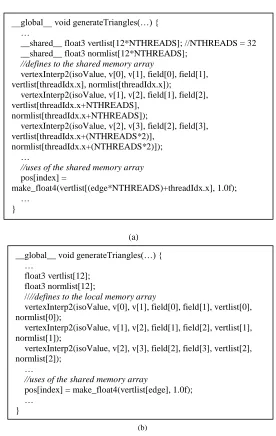
The benchmark MC has multiple kernels and the kernel ‘generateTriangles’ dominates the performance. For this kernel, each TB has 32 threads and the launched grid contains 1024 TBs. The code segment of this kernel is shown in Figure 2.6a. It uses two shared memory arrays, ‘vertlist’ and ‘normlist’ for its intermediate results. The indices used to access these two arrays, as shown in Figure 2.6a, are ‘threadIdx.x + i*NTHREADS’, where ‘NTHREADS’ is 32 and ‘i’ ranges from 0 to 11. As a result, the data stored in these two shared memory arrays are actually not shared among different threads in a TB. Instead, each thread uses a part of each array for its own intermediate data. Therefore, we can replace these two shared-memory arrays with local-memory arrays, which are private to each thread, and use the L1 D-cache to buffer such local memory arrays. The code utilizing the local-memory arrays is shown in Figure 2.6b. The main reason why the local-memory arrays are used rather than global-memory arrays is that the L1 D-cache in the Fermi architecture uses a write-back write-not-allocate policy for local memory data.
shared-memory version due to the write-back write-not-allocate policy. Our experiments on GPGPUsim also report similar performance trends.
Figure 2.6. The code segment of the benchmark Matching Cube (MC). (a) The shared-memory version, (b) the D-cache version.
In summary, for the benchmark MC, the non-sharing usage of its shared-memory arrays enables them to be replaced with local-memory arrays. The key reason why the D-cache
__global__ void generateTriangles(…) { …
__shared__ float3 vertlist[12*NTHREADS]; //NTHREADS = 32 __shared__ float3 normlist[12*NTHREADS];
//defines to the shared memory array
vertexInterp2(isoValue, v[0], v[1], field[0], field[1], vertlist[threadIdx.x], normlist[threadIdx.x]);
vertexInterp2(isoValue, v[1], v[2], field[1], field[2], vertlist[threadIdx.x+NTHREADS],
normlist[threadIdx.x+NTHREADS]);
vertexInterp2(isoValue, v[2], v[3], field[2], field[3], vertlist[threadIdx.x+(NTHREADS*2)],
normlist[threadIdx.x+(NTHREADS*2)]); …
//uses of the shared memory array
pos[index] =
make_float4(vertlist[(edge*NTHREADS)+threadIdx.x], 1.0f); …
}
__global__ void generateTriangles(…) { …
float3 vertlist[12]; float3 normlist[12];
////defines to the local memory array
vertexInterp2(isoValue, v[0], v[1], field[0], field[1], vertlist[0], normlist[0]);
vertexInterp2(isoValue, v[1], v[2], field[1], field[2], vertlist[1], normlist[1]);
vertexInterp2(isoValue, v[2], v[3], field[2], field[3], vertlist[2], normlist[2]);
…
//uses of the shared memory array
pos[index] = make_float4(vertlist[edge], 1.0f); …
}
(a)
version outperforms the shared-memory version is that the D-cache version eliminates the shared-memory usage, which in turn removes the resource limitation on the number of concurrent TBs on each SM. Such improved TLP leads to higher performance for MC.
2.3.4 Case Study IV: Path Finder (PF)
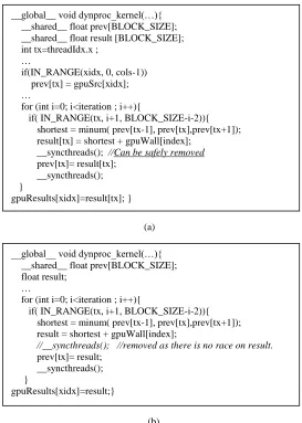
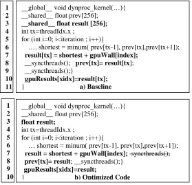
The kernel code of the benchmark Path-Finder makes use of two shared memory arrays, ‘prev’ and ‘result’, as shown in Figure 2.7a. Its TB dimension is 256x1 and its thread grid size is 19x1. As a result, the sizes of these two shared-memory arrays are small (256x4=1kB) and such shared memory usage is not a bottleneck for the number of concurrent TBs on each SM. For the shared-memory array ‘prev’, its accesses in the kernel code, ‘prev[tx-1]’ and ‘prev[tx+1]’indicate that the data in this array are shared among different threads. In contrast, the shared-memory array ‘result’ is always accessed with ‘result[tx]’, which means that there is no data sharing for this array. Therefore, we can simply use a register variable to replace it, as shown in Figure 2.7b. Further, as the variable is only defined and used in the same thread, we can safely remove the synchronization instruction ‘__syncthread()’ after the statement defining the variable ‘result’, as shown in Figure 2.7b. The same argument can also be made to remove the ‘__synchthread()’ instructions after defining the ‘result’ array element, as shown in Figure 2.7a.
However, if we replace the prev array in shared memory with a global-memory array, the performance would degrade by 15.7%. . This is mainly because re-accessing the frequently updated prev array in each loop hurts the cache performance with the WE policy.
Figure 2.7 The code segment of the benchmark Path-Finder (PF). (a) The shared-memory version, (b) the D-cache version.
In summary, for the benchmark PF, as one of its shared-memory array is not used for data communication across different threads, this shared-memory array can be replaced with register variables. The register variables have the lowest access latency and it also takes fewer
__global__ void dynproc_kernel(…){ __shared__ float prev[BLOCK_SIZE]; __shared__ float result [BLOCK_SIZE]; int tx=threadIdx.x ;
…
if(IN_RANGE(xidx, 0, cols-1)) prev[tx] = gpuSrc[xidx]; …
for (int i=0; i<iteration ; i++){
if( IN_RANGE(tx, i+1, BLOCK_SIZE-i-2)){ shortest = minum( prev[tx-1], prev[tx],prev[tx+1]); result[tx] = shortest + gpuWall[index];
__syncthreads(); //Can be safely removed
prev[tx]= result[tx]; __syncthreads(); }
gpuResults[xidx]=result[tx]; }
__global__ void dynproc_kernel(…){ __shared__ float prev[BLOCK_SIZE]; float result;
…
for (int i=0; i<iteration ; i++){
if( IN_RANGE(tx, i+1, BLOCK_SIZE-i-2)){ shortest = minum( prev[tx-1], prev[tx],prev[tx+1]); result = shortest + gpuWall[index];
//__syncthreads(); //removed as there is no race on result.
prev[tx]= result; __syncthreads(); }
gpuResults[xidx]=result;}
(a)
instructions to access registers than accessing shared-memory variables. Both lower latency and fewer dynamic instructions make the D-cache version outperform the shared-memory version for PF.
2.4 Experiments
2.4.1 Experimental Methodology
Table 2.1. The GPGPUsim configuration.
# of execution cores 15
SIMD Pipeline Width 16
Number of Threads/Core 1536
Number of
Registers/Core 32768
Shared Memory /Core 16kB/48kB: 32 banks; 3-cycle latency; 1 access per cycle
L1 Data cache/Core
16kB: 128B line, 4-way assoc 48kB: 128B line, 6-way assoc
1-cycle hit latency
MSHR Entry 128 entries
Constant Cache Size
/Core 8k
Texture Cache Size/Core 12k , 128B line, 24-way assoc L2 Data cache 768k: 128B line, 16-way assoc Number of Memory
Channels 6
Memory Channel
Bandwidth 8 Bytes/Cycle
DRAM clock 1400 MHz
DRAM Schedule Queue
Size 16 , Out of Order ( FR-RCFS) Warp Scheduling Policy Greedy then oldest scheduler
memory for the L1 D-cache versions and 16kB L1 D-cache + 48kB shared memory for the shared-memory versions.
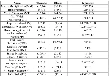
Table 2.2 The benchmarks used in experiments.
Name Threads Blocks Input size
Matrix Multiplication(MM) (16,16) (16,16) 256*256 Histogram(HG) (64,1) (128,1) 1024*1024 Matrix Transpose(MT) (16,16) (64,64) 1024x1024
Fast Walsh
Transform(FWT) (512,1) (4096,1) 8388608 3D Laplace Solver(LPS) (32,4) (4,25) 100*100*100 Needleman-Wunsch(NW) (16,1) (64,1) 1024*1024*10
Back Propagation(BP) (16,16) (16,16) 65536 scalar product of
vectors(SP) (64,1) (256,1) 8192*512 Fast Fourier
Transform(FFT) (64,1) (4096,1) 4k*1k Discrete Wavelet
Transform(DWT) (512,1) (256,1) 256k
Image Blur(Blur) (256,1) (2,512) 1k*1k StoreGPU(STO) (128,1) (384,1) 196656
Matrix-Vector
Multiplication(MV) (32,1) (64,1) 2048*2048 MarchingCubes(MC) (32,1) (1024,1) 32768
N-Queue Solver(NQU) (96,1) (256,1) 8
Path Finder(PF) (256,1) (19,1) 4096*100*20
variables. The second category includes the benchmarks STO, MV, MC, NQU, and PF. The remaining applications fall into the first category.
For a benchmark, if its shared-memory version limits the number of concurrent TBs on each SM, its corresponding D-cache version will have no such a constraint. In such cases, we allocate an unused shared-memory array to control the number of concurrent TBs to run on each SM. Then, we pick the best performing TB number for the D-cache version of the benchmark. More details on the TB number are discussed in Section 2.4.4.
2.4.2 Experimental Results on GTX 480 and GTX680 GPUs
We first present a performance comparison between the shared-memory versions and the cache versions on the GTX 480 GPU. As shown in Figure 2.8, the execution time of the D-cache version of each benchmark is normalized to the execution time of its corresponding shared-memory version. From the figure, we can see that on GTX 480, among the 16 benchmarks in our study, 14 benchmarks favor shared memory. Only two benchmarks, PF and MC, have higher performance with L1 D-cache versions than their shared-memory versions for the reasons discussed in Section III. On average, using the geometric mean (GM), the shared-memory versions result in 55.7% higher performance than the L1 D-cache versions.
Figure 2.8. Performance comparison between the shared-memory versions and the L1 D-cache versions on a GTX 480 GPU.
0% 50% 100% 150% 200% 250% 300% 350% 400% 450% 500%
HG FFT MV STO FWT LPS MT DWT NW MM NQU SP BP Blur PF MC GM
N
o
rm
al
ize
d
e
xec
. t
im
e
shared mem
Figure 2.9. Performance comparison between the shared-memory versions and the L1 D-cache versions on a GTX 680 GPU.
A performance comparison for the GTX 680 is presented in Figure 2.9. Compared to the Fermi architecture (i.e., GTX480), the Kepler architecture (i.e., GTX680) has more ALUs in each SM. Also, the L1 D-cache/shared memory in the Kepler architecture has a lower hit latency (33/33 cycles) than in the Fermi architecture (80/44 cycles). Unlike the Fermi architecture, global memory data are not cached in the L1 D-cache in the Kepler architecture. Despite these architectural differences, among the 16 benchmarks, only these same two benchmarks, PF and MC, achieve higher performance using the L1 D-cache version than the shared memory version.
2.4.3 Experimental Results on GPGPUsim
The performance comparison between the shared-memory versions and the L1 D-cache versions on GPGPUsim is presented in Figure 2.10. The performance for the L1 D-cache versions using both a write-evict (WE) policy and a write-back write-allocate (WBWA) policy are normalized to the performance of the shared memory versions. We also include the results of a fully associative L1 D-cache (FA+WBWA).
0% 50% 100% 150% 200% 250% 300% 350% 400% 450% 500% 550%
HG FFT MV STOFWT LPS MT DWTNW MMNQU SP BP Blur PF MC GM
N
o
rm
a
lized
exec.
t
im
e
Compared to the actual hardware, the L1 D-cache has a 1-cycle hit latency and shared memory has a 3-cycle access latency in our GPGPUsim model. As a result, some benchmarks, such as FFT, NQU, and Blur, show smaller performance gaps between the L1 D-cache versions and the shared memory versions than the GTX480/680 results. On the other hand, for the benchmark MV, GPGPUsim reports much higher performance gaps between the L1 D-cache versions and the shared memory versions than the GTX480/680 results. The reason is that the L1 D-cache in GPGPUsim uses a basic index function, which leads to high numbers of conflict misses for MV.
Figure 2.10 Performance comparison between the shared-memory versions and the L1 D-cache versions on GPGPUsim. The following cache models are evaluated for D-cache versions: 6-way 48kB with a write evict (WE) policy, 6-way 48kB with a write-back write-allocate (WBWA) policy, fully-associative 48kB with a WBWA policy (WBWA+FA).
Several interesting observations can be made from Figure 2.10. First, for most benchmarks, the shared memory versions have higher performance than the D-cache versions, which is consistent with the real hardware results shown in Figure 2.8 and Figure 2.9.
0% 100% 200% 300% 400% 500% 600% 700% 800%
HG FFT MV STO FWT LPS MT DWT NW MM NQU SP BP Blur PF MC GM
Norm
al
iz
e
d
Ex
e
c.
Ti
m
e
shared mem
L1 D (WE)
L1 D (WBWA)
Second, the WE policy hurts the cache performance if the updated data will be re-accessed again soon. This is the case for the benchmark FFT, as discussed in Section III-B. The benchmarks HG, MV, FWT, LPS, DWT, and BP also show similar behavior. Therefore, a WBWA policy can significantly improve the performance for these benchmarks. However, if the updated data will not be re-accessed, the WBWA policy may introduce cache pollution, thereby increasing the cache miss rate. The benchmarks STO, MT, and MC exhibit such a problem with the WBWA policy, as confirmed in the cache miss results presented in Figure 11.
Third, increasing set associativity reduces conflict misses and the benchmark MV drastically benefits from it. With the tiling optimization, the working set size of MV is within the cache capacity. However, its threads in a warp access the input matrix in a column-by-column manner. Therefore, given an input-matrix size of 2048x2048, different column-by-columns have
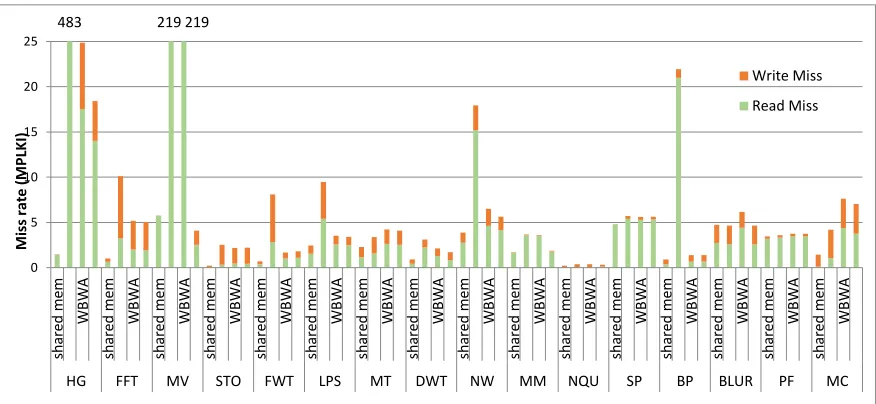
Figure 2.11. Cache miss rates of the shared-memory versions and the L1 D-cache versions on GPGPUsim. The following cache models are evaluated for D-cache versions: 6-way 48kB with a write evict (WE) policy, 6-way 48kB with a write-back write-allocate (WBWA) policy, fully-associative 48kB with a WBWA policy (WBWA+FA). The Shared Memory versions use a 4-way 16kB L1 D-cache.
0 5 10 15 20 25 sh ar ed m em W B W A sh ar ed m em W B W A sh ar ed m em W B W A sh ar ed m em W B W A sh ar ed m em W B W A sh ar ed m em W B W A sh ar ed m em W B W A sh ar ed m em W B W A sh ar ed m em W B W A sh ar ed m em W B W A sh ar ed m em W B W A sh ar ed m em W B W A sh ar ed m em W B W A sh ar ed m em W B W A sh ar ed m em W B W A sh ar ed m em W B W A
HG FFT MV STO FWT LPS MT DWT NW MM NQU SP BP BLUR PF MC
Write Miss Read Miss M is s rat e (M P LK I)
the same cache line indices, resulting in a high number of conflict misses. A fully associative cache eliminates the problem, as also confirmed in Figure 2.11.
Fourth, with a WE policy, the D-cache versions outperform the shared-memory versions only for the benchmarks PF and MC, which is also consistent with the actual hardware results. With a fully associative cache and a WBWA policy, the benchmarks MV, NQU, and PF show higher performance using the D-cache versions than the shared-memory versions. For MV, since there is no data communication among the threads, we use registers to buffer each tile of the input matrix. As discussed before, register accesses have a lower latency and require a smaller number of instructions than shared-memory accesses. Furthermore, using registers eliminates the need for coalescing to perform column-based accesses. Therefore, the D-cache version using a fully associative cache for MV outperforms the corresponding shared-memory version. As discussed in Section III-C, the D-cache version for the benchmark MC benefits from increased TLP, thereby resulting in higher performance than its shared-memory version. The benchmark NQU also shows similar behavior to MC.
In Figure 2.11, we compare the cache performance, measured as misses per kilo instructions (MPKI), between the shared-memory versions and the D-cache versions. Note that the shared-memory versions still utilize the L1 D-cache when they access global memory or local memory. Also, for the shared-memory versions, the L1 D-cache size is 16kB. From Figure 2.11, we can see that the shared-memory versions typically have low cache miss rates, indicating that most data accesses are satisfied with shared memory. For the D-cache versions, a WBWA policy reduces the misses caused by write-evictions but may hurt some benchmarks as discussed before. From Figure 2.10 and Figure 2.11, we can also see that TLP significantly mitigates the performance impact of cache misses.
2.4.4 The TLP Impact of the D-Cache Versions
the performance results measured on the GTX 480 GPU are shown in Figure 2.12. The results on the GTX680 GPU and GPGPUsim show similar trends. Among these benchmarks, the maximal number of concurrent TBs per SM is 4 for the benchmark STO due to its register usage. For the remaining four benchmarks, up to 8 TBs can be dispatched to an SM, where 8 is a hardware limit [3]. From Figure 2.12, we can see that the benchmarks MC and STO prefer more TBs or higher TLP. For NQU, the TLP impact is relatively small as long as there are at least 3 TBs in each SM. For benchmarks FFT and HG, the best performance is achieved with 4 TBs and 6 TBs per SM, respectively. Further increasing the number of TBs per SM will result in cache contention, thereby hurting performance.
Figure 2.12 The execution time of D-cache versions with different numbers of concurrent TBs per each SM. The execution times are normalized to the execution time of the shared-memory versions.
2.4.5 Impact on Energy Consumption
We use GPUWattch [51] to analyze the impact of using shared memory vs. L1 D-cache on energy consumption and the results are in Figure 2.13. Similar to our performance comparison, we include the energy consumption results for L1 D-cache versions using a write-evict (WE) policy, a write-back write-allocate (WBWA) policy, and a fully associative write-back write
0% 100% 200% 300% 400% 500% 600% 700% 800%
FFT MC HG STO NQU
2 TBs 3TBs 4 TBs
5TBs 6 TBs
7TBs 8 TBs
Norm
al
iz
e
d
Ex
e
c.
Ti
m
allocate L1 D-cache (FA+WBWA). The energy of D-cache versions is normalized to the energy of the shared memory versions.
As shown in Figure 2.13, the trend on energy matches the performance trend shown in Figure 2.10 for most benchmarks due to the significant static energy consumption modeled in GPUWattch and the lack of speculative execution in GPUs. One interesting exception is the D-cache version for the benchmark MC. The D-cache version enables more concurrent thread blocks (TB) and has lower execution time than its shared memory version. However, the high number of TBs leads to cache contention and results in higher dynamic energy consumption in memory hierarchy. Therefore, for MC, the D-cache version, although with lower execution time, consumes more energy than the shared-memory version.
Overall, for most of the benchmarks, the shared memory version consumes less energy than the D-cache version. On average, the shared memory versions consume 48.5% energy compared to the D-cache versions with a WE policy, 53.7% energy compared to the D-cache versions with a WBWA policy, and 71.9% of energy compared to the D-cache versions with a FA and a WBWA policy.
Figure 2.13 Energy comparison between the shared-memory versions and the L1 D-cache versions on GPUWattch. The following cache models are evaluated for D-cache versions: 6-way 48kB with a write evict (WE) policy, 6-way 48kB with a write-back write-allocate (WBWA) policy, fully-associative 48kB with a WBWA policy (WBWA+FA).
0% 100% 200% 300% 400% 500% 600% 700% 800%
No
rm
a
lized
E
nerg
y shared mem
L1D(WE)
L1D(WBWA)
2.4.6 Summary
In summary, from our experiments on both real hardware and architectural simulators, we can derive the following important insights. First, MLP and coalesced accesses are key reasons for the shared-memory versions to outperform the D-cache versions. Second, for D-cache versions, the D-cache write policy and D-cache contention may have a strong impact on performance. Third, eliminating shared-memory usage enables higher TLP and more opportunities to allocate variables to registers, which are the key reasons for the D-cache versions to outperform the shared-memory versions.
2.5 Related Works.
To the best of our knowledge, our work is the first to study the tradeoffs between software-managed cache and hardware-software-managed cache on GPU architectures. The most related work is by Jia et al. [36], who observed that the L1 D-caches are not always helpful for GPGPU performance. They identified as a reason that data fetched at the cache-line granularity may consume too much bandwidth if data reuses are limited. They also propose a compiler-time approach to predict the D-cache’s performance impact and then to turn on/off the D-cache accordingly. In comparison, we focus on comparing the effectiveness between the D-cache and shared memory. For our benchmarks, the D-cache versions are developed directly from the shared memory versions such that the cached data have strong data reuse, which lead us to identify different performance tradeoffs.
hardware-managed caches. As shown in our experimental analysis, TLP, MLP, and coalescing have a strong performance impact while such factors are non-existent in embedded systems.
Current works on GPU memory hierarchy mainly focuses on how to improve performance. There have been approaches proposed to utilize shared memory to convert un-coalesced accesses into coalesced ones[87]. The TLP limit introduced by shared memory usage is addressed by timing-multiplexing shared memory [88]. Cache contention among warps has been observed in [66] and a cache-conscious warp scheduling algorithm is proposed to address this problem.
2.6 Conclusions
Chapter 3
Automatic Data Placement into GPU On-Chip
Memory Resources
3.1 Introduction
resources are complex and sometimes non-intuitive [57]. More importantly, as on-chip resources have been changing significantly for different generations of GPUs, an optimized kernel upon one generation becomes suboptimal on another one. Thus performance portability is a daunting challenge for application developers.
In this work, we propose compiler-driven automatic data placement as our solution. We focus on GPGPU programs that have already been reasonably optimized either manually by programmers or automatically by some compiler tools. In other words, our input programs already employ classical loop optimizations such as tiling and allocate important data, either for communication among threads or for data reuses, in shared memory. Our proposed compiler algorithm refines these programs by revising data placement across different types of GPU on-chip memory resources.
over-utilize shared memory while underutilizing the register file when it runs on GT200 or KEPLER GPUs. As a result of such underutilization, it is proposed in prior works [10] to turn off significant portions of the register file to reduce static power consumption.
We evaluate our proposed automatic data replacement algorithm using a diverse set of applications from different GPGPU benchmark suites that have been manually optimized. Our results show that our compiler algorithm improves the performance by up to 4.14X and an average 1.76X on the FERMI architecture, and by up to 3.30X and an average of 1.61X on the KEPLER architecture.
The remainder of the chapter is organized as follows. Section 3.2 presents a brief background on GPU architecture with an emphasis on on-chip memory resources. Section 3.3 presents in detail our proposed automatic data placement algorithm. Section 3.4 and 3.5 discuss our experimental methodology and the experimental results. Section 3.6 addresses the related work. Section 3.7 concludes this chapter.
3.2 Background and Motivation
State-of-the-art GPUs employ many-core architecture, on which the cores are organized in a two-level hierarchy. Each GPU contains a cluster of streaming multiprocessors (SM) in Nvidia GPUs, or computing units in AMD GPUs. Each SM in turn consists of multiple streaming processors (SPs). To amortize the overhead of instruction fetch and decode, an array of SPs executes one scalar program in the single-instruction multiple-data (SIMD) manner. A group of threads running on such an array of SPs and sharing the same program counter (PC) is referred to as a warp of threads. Multiple warps of threads are grouped into a thread block (TB) and a number of thread blocks are organized into a thread grid.
In order to reduce the latency and improve the bandwidth of off-chip memory accesses, three types of on-chip memory including shared memory, data caches, and a register file, are introduced in each SM. Texture caches and constant caches are also on-chip memory but they are used for read-only data and not our focus in this study.
Among three types of on-chip memory, the register file has the shortest access latency and highest throughput. Furthermore, the register file is larger than the L1 D-cache and shared memory as shown in Table 3.1. The register file is private to each thread, which means data in registers can only be accessed by a single thread, except for the latest Nvidia KEPLER architecture, which introduces a new instruction “__shfl” [4] to enable a thread to access the registers in other threads within the same warp. The maximum number of registers per thread is ISA-dependent and varies in different architectures. Exceedingly heavy usage of registers per thread will result in register spills into its local memory, which may be captured in L1 D-cache.
Compared to register files, shared memory has lower throughput and smaller capacity. As shown in Table 3.1, a GTX 680 GPU has a 256KB register file and 48KB shared memory. As shared memory is accessible to all threads in a TB and has low access latency, prior works have been focused on using shared memory to achieve memory coalescing, to provide data communication, and to store data for temporal reuses. L1 D-cache shares the same hardware resource as shared memory on FERMI or KEPLER architecture, in contrast to shared memory, which is explicitly managed by kernel code, L1 D-caches are hidden from developers and are implicitly managed by hardware to keep the most recently accessed data. Furthermore, while the intensive usage of shard memory or registers can limit the number of threads running on each SM, the usage of L1 D-cache does not. However, too many threads in a SM would compete with each other for the limited L1 D-cache capacity, which may result in poor performance due to cache contention [42].
in computational throughput than off-chip memory bandwidth. For example, from the FERMI architecture to the KEPLER architecture, the computation throughput increases by up to 229% while the memory bandwidth increases by only 8.3%. As a result, we need to more carefully manage on-chip resource to effectively utilize the computational resources. Second, among GPU on-chip memory resources, the register file size and D-cache/shared memory have been changing across different generations. For example, From G80 to GT200, the register file size is doubled while the shared memory capacity remains the same. The same trend is present when comparing the FERMI architecture and the KEPLER architecture. Consequently, the code optimized for early GPU generations tend to use shared memory more heavily. This leads to a serious challenge for performance portability for such optimized code running on different GPUs.
Table 3.3. A comparison of hardware characteristics across different GPU generations.
G80 (GTX 8800)
GT200 (GTX 280)
FERMI (GTX 480)
KEPLER (GTX 680)
KEPLER (K20c)
Arithmetic throughput
(Gflops/S) 504 933 1345 3090 3950
Memory Bandwidth
(GB/S) 57 141 177 192 250
Shared memory size(KB) 16 16 48 48 48
Register file size(KB) 32 64 128 256 256
3.3 Automatic Data Placement into On-chip Memory Resources
To automatically manage on-chip memory resources and achieve performance portability, in this section, we describe in detail our proposed compiler algorithm for automatic data placement. We first present our analysis of possible data placement patterns among different types of on-chip memory resources. Then, we construct our compiler algorithm using the profitable patterns.
3.3.1 Data Placement Patterns
Pattern 1: Promote variables from shared memory to registers
Shared memory can be used to exchange data among threads in a TB. Also, as a low-latency on-chip resource, many applications use shared memory as software-managed cache to hold important (private) data for each thread. There are three reasons why it may be profitable to promote a shared memory variable into registers. First, the shared memory usage may limit the number of concurrent TBs on an SM, i.e., TLP, and promoting shared memory variables into registers can alleviate the pressure on this critical resource. Second, shared memory has longer access latency and lower bandwidth than register files. Third, accessing shared memory variables is associated with instruction overhead for address computations. Therefore, higher performance may be expected when promoting shared memory variables into registers.
Register variables
Shared memory variables
Local/global variables in L1 D-caches
1
2 3 4
5
6
We show a benchmark, PathFinder, as an example, in Figure 3.2. Path-Finder makes use of two shared memory arrays, ‘prev’ and ‘result’, as shown in Figure 3.2. Its TB dimension is 256x1 and its thread grid size is 19x1. As a result, the sizes of these two shared-memory arrays are small (256x4=1kB) and such shared memory usage is actually not a bottleneck for the number of concurrent TBs on each SM. For the shared-memory array ‘prev’, its accesses in the kernel code, ‘prev[tx-1]’ and ‘prev[tx+1]’indicate that the data in this array are indeed shared among different threads. As shown in line 7 in Figure 3.2a, the ‘result’ array is accessed by each thread multiple times in a loop. As each thread only accesses the array result using its own thread id as shown in line 8 and line 9 in the figure, there is no communication using the ‘result’ array across threads. Since each thread only accesses its individual part of the array, it is safe to simply replace ‘result[tx]’ with a register. Further, as the variable is only defined and used in the same thread, we can safely remove the synchronization instruction ‘__syncthread()’
1 2 3 4 5 6 7 8 9 10 11 12
__global__ void dynproc_kernel(…){ __shared__ float prev[256];
__shared__ float result [256];
int tx=threadIdx.x ;
for (int i=0; i<iteration ; i++){
…. shortest = minum( prev[tx-1], prev[tx],prev[tx+1]);
result[tx] = shortest + gpuWall[index];
__syncthreads(); prev[tx]= result[tx]; __syncthreads();}
gpuResults[xidx]=result[tx];
} a) Baseline
1 2 3 4 5 6 7 8 9 10 11
__global__ void dynproc_kernel(…){ __shared__ float prev[256];
float result;
int tx=threadIdx.x ;
for (int i=0; i<iteration ; i++){
… shortest = minum( prev[tx-1], prev[tx],prev[tx+1]);
result = shortest + gpuWall[index]; syncthreads();
prev[tx]= result; __syncthreads();}
gpuResults[xidx]=result;
} b) Optimized Code