The Dependence of Coating Characteristics on Progress Parameters
and Alloy Compositions
Olga. P. Terleeva
1, Young-Joo Oh
2*, Myoung-Ryul Ok
2, Vladimir V. Utkin
1,
Heon-Phil Ha
2and Dong-Heon Lee
31Institute of Inorganic Chemistry, Siberian Branch, Russian Academy of Sciences, Acad. Lavrentyev Ave., Novosibirsk, 630090 Russia
2Metal Processing Research Center, Korea Institute of Science and Technology, 39-1 Hawolgok-dong, Seongbuk-gu, Seoul, 136-791 Korea
3International Metal Institute, Inc., 392-1 Gocheondong Uiwang City, Gyeonggido, 437-801 Korea
The coating characteristics on the surfaces of the aluminum alloys A1230, A2017, Al–7.6 mass%Si, and Al–10.4 mass%Si formed at AC polarization were investigated. The intervals of current densities and process durations were checked, and data consisting of coating thickness and increases in size and weight were obtained. The presence of the high-temperature aluminum oxide phases, which provide high physical-mechanical coating characteristics, was registered with the help of the Bruker D8 Advanced X-ray diffractometer.
(Received July 11, 2005; Accepted September 21, 2005; Published November 15, 2005)
Keywords: microplasma-electrochemical process, aluminum alloy, oxide coating
1. Introduction
The microplasma electrochemical process (MEP) is a method of producing oxide-ceramic coatings that is more advanced than the conventional anodization. Discrete light phenomena were first studied by Russian scientist N. P. Sluginov,1) then by German investigators A. Guntershulze and H. Betz2)and American scientists L. L. Gruss and W. J. McNeil,3,4) but highly protective properties have not been studied. In the 1970s, G. A. Markov revealed the process parameters of intervals and electrolyte compositions in which specific microdischarges appear. These microdischarges can provide high-quality microplasma coatings.5) The
micro-plasma processes, however, did not attract considerable attention until Russian and English scientists organized the companies in Western Europe. Since then, the MEP (the so-called PEO (plasma electrolytic oxidation)6)) has been
in the spotlight all over the world. The dependence of the coating characteristics on alloy composition are known,7,8) but such data are incomplete and rudimentary
because less data are available on AC polarization than on DC polarization. Systematic investigations are needed to develop the models and theories that may forecast new coating properties using AC polarization. This paper is devoted to this purpose.
2. Experimental Procedure
The cylindrical stainless steel bath was equipped with a water-cooled jacket and an airlift, which kept the electrolyte temperature at 40C throughout the process and which also
served as a counter electrode.
Disk samples, each with an area of 25 cm2, were made of
Al alloys of industrial-grade A1230 (above 99.3 mass% Al), A2017 (3.8 to 4.8 mass% Cu). Al–7.6 mass%Si alloy and Al– 10.4 mass%Si alloy were also used. No samples received heat treatment because the coating characteristics depend on the heat treatment of aluminum-silicon alloys.8) The samples were placed 50 mm from the surface of the electrolyte and
were subjected to microplasma treatment under AC sinus-oidal polarization with a frequency of 50 Hz. The anodic and cathodic currents have same amplitudes.
The voltage-time and current-time curves of the cathode and anode were registered for AC polarization. AC polar-ization was applied under anodic current densities (jan) of
20–1440 A m2. After the treatment, the samples were rinsed
thoroughly with water and were dried with hot air.
An aqueous electrolyte was prepared using solid potassium hydroxide. During the process, the visual characteristic changes of the microdischarge—the color and dimension of microdischarges and the character of the discharge move-ment on the sample surface—were also analyzed. These data are usually required to register the qualitative differences of process stages.
The increase in a sample weight was measured with
0:0002g accuracy using an analytical balance.
The phase composition of the surface layer was studied using a Bruker D8 Advanced X-ray diffractometer (Cu K
radiation) at a fixed incident angle of 20 in the 2¼
20{100 range, with 0.02steps and a 4/min scan rate.
The coating thickness was measured with the help of a thickness gauge with 5% accuracy. For the calculation of small coating thickness values (below 2.5mm), the following empirical equation was used:
Th¼2:2CAC0:12
S t;
mFAmin cm2 ;
whereThis the coating thickness,CACis the capacity of the
power supply unit (mF),tis the process duration (min), andS
is the sample area (cm2). The increase in linear size was also
registered. For this purpose, the linear sizes of the pre- and post-treatment samples were measured using a micrometer with an accuracy of5mm.
3. Results and Discussion
3.1 The dependence of the coating thickness and the increase in linear size on the process duration, current density, and alloy composition
The low and high current densities provided the different
*Corresponding author, E-mail: [email protected]
thermal conditions on a sample surface. It is known that the rates of the chemical and anodic dissolution of aluminum in an electrolyte, the growth rate of coating layers, and the increase in weight and phase compositions may depend on thermal conditions. In Fig. 1, both the experimental and calculated dependence of the thicknesses of the coating layers are given. It can be seen that the thicknesses of the coating layers increase with an increase in anode current density. The experimental thickness dependence coincides with the calculated dependence within the experimental error of the measurement for thin coating (below 2.5mm).
Figure 2 shows a set of thickness dependence on the different aluminum alloys and the different anode current densities. It would be observed that both the process duration and anode current density caused an increase in coating thickness. Based on the data in Figs. 1 and 2, it can be said with certainty that the thicknesses of the coating layers
0 100 200 300 400
0 2 4 6 8 10
Thickness, Th/
µ
m
Anode current density, Jan/ Am-2
Experimental Calulated
Fig. 1 The dependence of coating thickness on the anodic current densities of the process. (AC mode, Ssamples¼0:25dm2,t¼40C,t¼30min)
0 1000 2000 3000 4000 5000 6000
0 20 40 60 80 100 120 140 160 180
(a)
Thickness, Th/
µ
m
Time, t/ s
J1 J2 J3
0 1000 2000 3000 4000 5000 6000
0 50 100 150 200 250
(b)
Thickness, Th/
µ
m
Time, t/ s J1 J2 J3
0 1000 2000 3000 4000 5000 6000
0 50 100 150 200 250
(c)
Thickness, Th/
µ
m
Time, t/ s
J1 J2 J3
0 1000 2000 3000 4000 5000 6000
0 20 40 60 80 100 120 140 160 180 200
(d)
Thickness, Th/
µ
m
Time, t/ s J1 J2 J3
Fig. 2 Time-thickness dependence on different anode current densities (j1¼600A/m2, j2¼1000A/m2, j3¼1400A/m2) and on different aluminum alloys: (a) A1230, (b) A2017, (c) Al–7.6 mass%Si, and (d) Al–10.4 mass%Si.
0 1000 2000 3000 4000 5000 6000
0 50 100 150 200 250
(a)
Thickness and Increase in size,
Th
/
µ
m
Time, sec Thickness J1
Delta J1 Thickness J2 Delta J2
Thickness J3 Delta J3
0 1000 2000 3000 4000 5000 6000
1.0 1.1 1.2 1.3 1.4 1.5
(b)
Ratio
Time, t/ s
Ratio 1 Ratio 2 Ratio 3
[image:2.595.313.540.73.247.2] [image:2.595.105.492.292.579.2] [image:2.595.105.489.620.760.2]increase monotonically and have no regular features. Notice that the growth rates of the thickness layers are reduced only slightly with an increase in anode current density.
The growth rates of the thickness layers vary based on alloy composition. A1230, A2017, and Al–10.4 mass%Si have approximately the same growth rates, but Al–7.6 mass%Si has a different one.
It is interesting to compare the changes in layer thickness with the changes in linear size [Figs. 3(a), (b)]. A change in linear size means a difference in linear size of sample between before and after MEP and has originated only from the substances of electrolytes. At the beginning of the microplasma process, the thickness of the coating layer and the increase in linear size of a sample were almost the same. This can explain the following two points: (i) the coating was formed at the cost of an electrolyte substance and the substrate was not dissolved; and (ii) the etching processes, the oxidizing processes of the substrate surface and the electrolyte substance thickening on the substrate surface were balanced such that the thicknesses of the coating layers were virtually equal to the increases in the linear sizes of the samples within the experimental margin of error.
The ratio of thickness/size increased with an increase in the duration of the microplasma process and in the anode current density [Fig. 3(b)]. This means that the ratio increases with growing coating thickness. These trends are the same for other aluminum alloys.
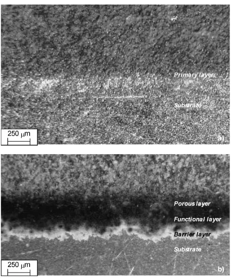
The microscopic investigation of a cross-section of coating layers provided no evidence of the presence of a different structure in the coating layers at the beginning of the microplasma process [see Fig. 4(a)]. At the late stages of the process, three coating layers were clearly defined [see
Fig. 4(b)]. This fact has already been described as follows;9) Porous layers are always produced in silicate electrolytes and located in an outer side, functional layers have high protective characteristics and barrier layers are main barriers for currents and always produced in all electrolytes.
The X-ray analysis shows that the phases of coating layers
Fig. 4 A cross-section of the coating layers: (a) 180 s, and (b) 3300 s.
0 5 10 15 20
0.0 0.5 1.0 1.5 2.0 2.5 3.0 3.5
(a)
Delta W, g
Charge passed, Q/kC
J1
J2 J3
0 5 10 15 20
0.0 0.5 1.0 1.5 2.0 2.5 3.0 3.5
(b)
Delta W, g
Charge passed, Q/kC
J1
J2 J3
0 5 10 15 20
0.0 0.5 1.0 1.5 2.0 2.5 3.0 3.5
(c)
Delta W / g
Charge passed, Q/kC
J1 J2 J3
0 5 10 15 20
0.0 0.5 1.0 1.5 2.0 2.5 3.0
(d)
Delta W / g
Charge passed, Q/kC
J1 J2 J3
Fig. 5 The increase in a sample weight (W) on the charges passed (Q) for different anode current densities (j1¼600A/m2,
[image:3.595.312.542.158.434.2] [image:3.595.111.485.471.759.2]are represented by a small quantity of gamma aluminum oxide and amorphous phase silicon oxide at the start of the process (180s).
3.2 The dependence of the increase in sample weight on anode current density, process duration, and alloy composition
The increase in sample weight (W,g) tends to increase with an increase in the quantity of the charge passed (Q,kC) and in the anode current density (Fig. 5).
As for different alloys, the W has the same level for A1230, A2017, and Al–7.6 mass%Si, and a lower level for Al–10.4 mass%Si. This means that the high silicon content in alloys hinders coating growth.
A microscope analysis of the sample surface containing high Silicon showed that there appeared individual silicon particles or silicon accumulations. The linear dimensions of such silicon sections (or silicon particles) on the sample surface can exceed 100mm.8)The data obtained in this paper
confirmed that these dimensions of silicon have an adverse effect on the microplasma process.8,10) An explanation for
this was found in the following reference:8)‘‘The hindering of
the growth of the oxide layer by silicon particles in the microarc oxidation of aluminum-silicon alloys is caused by the higher electrical resistivity of silicon with respect to the aluminum matrix.’’ This also means that the voltage for the
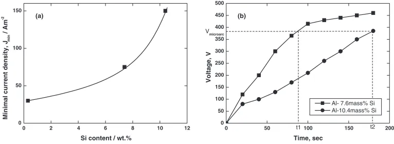
microplasma process of the Al–Si alloy must be higher where the silicon content is high than where it is low. A comparison of the anodic voltage-time curves of two alloys also shows (Fig. 6) that the anodic voltage of the Al–7.6 mass%Si alloy is higher than that of the Al–10.4 mass%Si alloy. Refer-ence 8), however, does not adequately explain this result. Another explanation of the adverse effect of accumulating silicon particles is thus offered herein. Pure silicon has electronic conductance and causes an increase in the leakage current.8) The leakage current raises the minimal anode
[image:4.595.56.283.403.570.2] [image:4.595.307.548.447.572.2] [image:4.595.106.489.619.759.2]current density to realize the microdischarge mode [Fig. 7(a)]. The second effect of the leakage current is that it extends the starting time of the microdischarge mode [Fig. 7(b)].
It is likewise believed that the formation process of a coating layer on the aluminum surface sections occurs at the conventional anodization stage as well as at the spark stage and at all the subsequent microplasma stages. The formation of a coating layer on the silicon surface sections does not start until the microplasma stage has been reached, which is when the thermochemical and plasma chemical reactions take place. There is circumstantial evidence of these conclusions in the paper.8)In this paper, data indicating that the coating
thickness on the aluminum surface section was higher than that on the surface of the silicon particles were registered.
3.3 The effect of process parameters and alloy compo-sition on the phase-coating compocompo-sition
Figure 8 shows the phase compositions of the coating layers for different durations of the microplasma process. At
0 1000 2000 3000 4000
400 450 500 550 600 650
Voltage, V
Time, sec
Al- 7.6mass% Si Al-10.4mass% Si
Fig. 6 The anode voltage-time curves for Al–7.6Si and Al–10.4Si (J¼ 1000A/m2, process duration = 55 min).
0 2 4 6 8 10 12
0 50 100 150
(a)
Minimal current density, J
min
/ Am
-2
Si content / wt.%
0 50 100 150 200
0 50 100 150 200 250 300 350 400 450 500
Vmicroarc
t2 t1
(b)
Voltage, V
Time, sec
Al- 7.6mass% Si Al-10.4mass% Si
Fig. 7 The dependence of (a) the minimal anode current density (jan) and (b) the extension of the starting time of the microdischarge mode
ðt1;t2Þon the Al–Si alloy composition (J¼600A/m2).
b)
a)
the beginning of the process, when the coating layer was thin (less than 3mm), only a small quantity of-phase Al2O3was
included [Fig. 8(a)]. The remains of the coating substance may be SiO2 or the oxide-hydroxide compounds of
alumi-num, which are amorphous. At the late stages of the process, the thickness of the coating layer increased (more than 160mm) and the presence of high-temperature - and -phases of Al2O3 are registered [Fig. 8(b)]. It is known that
the -phase of Al2O3 is the base of dense and high-quality
layers (the so-calledfunctional layer). The formation of this layer starts only after the critical thickness value of the primary coating layer has been obtained. For silicate-alkaline electrolytes, researchers6,10)reported that only a thick coating layer can accumulate enough heat to warm aluminum oxide up to the temperature of the-to--phase transition, and the critical values of the layers were 30–40mm.
If the aforementioned is the sole reason for the adverse effect of the accumulation of silicon particles on the microplasma process, a number of problems remain un-solved. It is not clear why the-to--phase transition is not observed in the coating layers produced at DC polarization in spite of the fact that the thicknesses of the layers are identical or higher at DC polarization than at AC polarization. The following results were also reported:11)a coating was initially
formed at DC polarization, and the -to--phase transition was not registered. When the same sample was again treated at AC polarization, however,-Al2O3 was obtained.
For a better understanding of the mechanism of the-to- -phase transition, it is necessary to also consider the other electrochemical and chemical processes connected to the action of a negative (cathodic) current, as well as the overcharging effect and hydrogen liberation described in reference.8)
It is believed that another effect of cathodic currents that was not considered in reference6) takes place at AC
polar-ization and results in the synthesis of specific amorphous oxide-hydroxide layers under a primary coating.
It is well known12)that a thin primary oxide or any ceramic
film (above 0.5mm) starts to be synthesized as a specific amorphous oxide-hydroxide layer between a primary oxide and metal surface at negative polarization (cathodic polar-ization). The thickness of this specific amorphous oxide-hydroxide layer can exceed 500mm. A key feature of this layer is the absence of unipolar conductivity therein. The growth of the oxide-hydroxide layer is accompanied by an increase in electrical resistance and process voltage until cathodic microdischarges appear. When heated up to 1200C, this oxide-hydroxide layer containing polymer
chains of boehmite and hydrargillite links was transformed into the-phase and then into the-phase of Al2O3.
On a basis of the above data, it is herein hypothesized that the effect of the cathodic current on the coating layer is the same at AC polarization and at negative DC polarization. When the primary coating thickness exceeds 30mm, a polymer oxide-hydroxide layer starts to form. This layer can act as the precursor of the -to--phase transition.
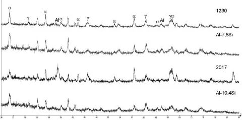
Figure 9 illustrates the results of an X-ray analysis of the coatings of four aluminum alloys. The identification of spectra is given only for the- and-phases of Al2O3. For
different aluminum alloys, it can be noted that all coating layers involve - and-phases of Al2O3. This means that
the basic phases of the coating layers responsible for high physical-mechanical properties13) are independent of
the alloy composition. As indicated above, the alloy com-position affects only the coating thickness.
4. Conclusions
It has been shown that coating thickness increases together with anode current density. The experimental thickness dependence (within the range of 1–2.5mm) coincides with the calculated dependence within the experimental error of measurement.
The growth rates of thickness decrease slightly with an increase in anode current density. A1230, A2017, and Al– 10.4 mass%Si have approximately the same growth rates, but Al–7.6 mass%Si has a different one.
The ratio of thickness/size increases with an increase in the duration of the microplasma process and in anode current density.
The W tends to increase with an increase in anode current density and in the charge passed. The high silicon content in aluminum alloys hinders coating growth.
It is suggested that the adverse effect of the accumulation of silicon particles manifests itself in the high leakage current. It results in an increase in anodic current density and process duration for the same coating layer.
The growth of the coating layer on the silicon surface sections starts only at the microplasma stages, when the thermochemical and plasma chemical reactions take place.
The thin coating layer contains a small quantity of-phase Al2O3. The main coating substance may be SiO2 or the
oxide-hydroxide compounds of aluminum, which are amor-phous. At the late process stages, the coating layer also contains the-phase of Al2O3.
The basic phases of the coating layers are independent of the alloy composition.
The key effect of the cathodic current is the synthesis of specific amorphous oxide-hydroxide layers under a primary coating, and the -to--phase transition is initiated on that layer.
[image:5.595.307.547.76.195.2]Acknowledgments
The authors are grateful to V. I. Kirillov for the valuable assistance he extended to the authors with regard to the experiments conducted in the study.
REFERENCES
1) N. P. Sluginov and Z. Russkogo: Physiko-Khimicheskogo obschestva 10(1898) 241–243.
2) A. Guntershulze and H. Betz:Electrolyticheskie kondensatori (Obor-ongiz, Moscow, 1938) pp. 6–56.
3) W. McNeil and R. Wick: J. Electrochem. Soc.105(1958) 544–547. 4) L. L. Gruss and W. J. McNeil: Electrochem. Technol.1(1963) 283–
287.
5) A. V. Nikolaev, G. A. Markov and B. I. Peschevitskiy: Izvestiya SO RAN SSSR Ser.him.nauk.5(1977) 32–33.
6) A. L. Yerokhin, L. O. Snizhko, N. L. Gurevina, A. Leyland, A. Pilkington and A. Matthews: J. Phys. D: Appl. Phys.36(2003) 2110– 2120.
7) V. Yu, A. V. Magurova and J. Timoshenko: Zaschita Metalov 31 (1995) 414–418.
8) M. M. Krishtal: J. Metal. Sci. Heat Treatment46(2004) 377–384. 9) V. I. Belevantsev, O. P. Terleeva, G. A. Markov, E. K. Schulepko, A. I.
Slonova and V. V. Utkin: Microplazmennie electrokhimicheskie proccessi. Obzor.34(1998) 468–484.
10) A. I. Slonova, O. P. Terleeva, E. K. Schulepko and G. A. Markov: J. Electrochim.25(1989) 1473–1479.
11) A. I. Slonova, O. P. Terleeva, E. K. Schulepko and G. A. Markov: J. Electrochim.28(1992) 1280–1285.
12) G. A. Markov, O. P. Terleeva and E. K. Schulepko: Izvestiya SO RAN SSSR Ser.him.nauk.3(1983) 31–34.