Depth-Resolved EELS and Chemical State Mapping
of N
þ-Implanted TiO
2Photocatalyst
Tomoko Yoshida, Shunsuke Muto and Jun Wakabayashi
Division of Quantum Science and Energy Engineering, Department of Materials, Physics and Energy Engineering, Graduate School of Engineering, Nagoya University, Nagoya 464-8603, Japan
We propose novel methods of depth-resolved EELS (DREELS) and chemical state mapping, and the techniques were applied to the cross-sectional TEM (XTEM) sample of Nþimplanted TiO
2catalyst. DREELS is realized by applying the Pixon deconvolution to a conventional
energy-filtering TEM (EFTEM)-based spatially resolved EELS (EFTEM-SREELS), demonstrated by Kimotoet al.[J. Electron Microsc.46
(1997) 369–374.]. And a self-modeling curve resolution (SMCR) technique in multivariate analysis enabled chemical state mapping from EFTEM-based spectrum imaging (EFTEM-SI) data sets. The methods successfully extracted the depth dependence of the N-KELNES and separately displayed the spatial distributions of the constituent chemical states, whose spectral features were overlapped.
[doi:10.2320/matertrans.MD200712]
(Received April 2, 2007; Accepted June 12, 2007; Published August 1, 2007)
Keywords: photocatalyst, visible-light response, ion implantation, electron energy loss spectroscopy, self-modeling curve resolution, energy-filtering transmission electron microscopy
1. Introduction
Transmission electron microscopy (TEM) and its associ-ated analytical techniques are now indispensable to materials analysis, especially to industrial R&D in nanotechnologies. Among other analytical techniques electron energy-loss spectroscopy (EELS) and energy-filtering TEM (EFTEM) have drastically developed during the latest decade to reveal the local electronic structures of nano-functional materials. The techniques taking the most advantage of a two-dimen-sional (2D) detector (charge-coupled devices, CCD) enabled spatially resolved EELS (SREELS), in which the energy filter of a line focus type is utilized and many spectra at different positions on the sample can be obtained simultaneously
without scanning the focused electron beam.1)Simultaneous
acquisition of the SREELS has an advantage in measuring small chemical shifts, because these measurements are not affected by instability of the accelerating voltage or a stray magnetic field. When applying the SREELS to a cross sectional TEM (XTEM) sample, each row of the 2D CCD image in the dispersion direction exhibits depth-selective EELS, though each single spectrum (corresponding to one row) usually suffers from its poor signal-to-noise and signal– to-background ratios (SNR and SBR) for a trace element, which practically requires averaging a number of rows in the cross-dispersion direction and consequently loses the spatial resolution.
In the mean time EFTEM has been useful for examining spatial distributions of particularly light elements, and it reveals even spatial distributions of specific chemical states by selecting the corresponding features in energy-loss near
edge structure (ELNES) with an energy slit.2) However,
ELNES ascribed to different chemical states are often overlapped over the same energy range, inseparable from the single spectrum. The EFTEM for chemical state mapping has been thus only effective when the ELNES of interest exhibits an appreciable chemical shift relative to that of the neighboring phases.
The purpose of the present study is to demonstrate the depth-resolved EELS (DREELS) and chemical state map-ping, by introducing modern mathematical treatments to the conventional SREELS and EFTEM-spectrum imaging (EF-TEM-SI), respectively. The methods then applied to nitrogen
ion-injected TiO2 photocatalyst to examine depth
depend-ence of the local chemical states of nitrogen injected:
photocatalytic reactions at the surface of TiO2under UV light
irradiation have been attracting much attention due to their applications such as self cleaning of tiles, glasses, and
windows.3–6)Recently, Asahiet al.reported that the
substitu-tional doping of N into TiO2 contributed to narrowing of
band gap, thus providing a visible-light response.7)
Further-more, previous investigations demonstrated that nitrogen doping increased optical absorption in the visible-light region and the absorbance evolved with increasing the nitrogen dose. The increase in the visible-light absorption, however, did not monotonically enhance the visible-light
responsive-ness.8,9) It is thus important to find the optimum local
concentration of doped nitrogen, as well as its chemical states effective for the visible-light responsiveness. In the present report, nevertheless, we focus mainly on the methodology of the techniques and the physical/chemical significance of the results will be discussed in a separate paper.
2. Experimental
2.1 Sample preparation
The samples used in this study were TiO2 (1 0 0) single
crystals of 550:5mm3 in size produced by Furuuchi
Kagaku, Japan. Mass analyzed 100 keV N2þ ions (50 keV/
Nþion) were injected into the samples at room temperature,
perpendicular to the sample surface. The Nþfluence ranged
from 1 to51021m2. A Monte Carlo calculation (by SRIM
code10)) indicated that the implanted N atoms were
distribut-ed up to180nm, and peaked around 90 nm in depth from
the surface. After the ion implantation, parts of the samples were heat-treated at 573 K for 7200 s in air. The
photo-Special Issue on Advances in Electron Microscopy for Materials Characterization
catalytic activity of the samples was evaluated from the color-fading rates of methylene-blue solutions by
visible-light irradiation ( >430nm) onto the samples immersed in
them.
Cross-section samples for observing the depth distribu-tions of N-related electronic structures were prepared: the irradiated sample was cut into half, and the two halves were pasted together face-to-face with epoxy glue. Then, this pasted slab was sectioned such that the damaged layers were visible, followed by dimpling and ion-milling according to standard sample preparation procedures for semiconductors and ceramics.
2.2 Depth-resolved EELS (DREELS)
EEL spectra were recorded with a Gatan ENFINA 1000 spectrometer attached to a JEM200CX TEM operated at 200 kV. The detecting system consists of a fiber-coupled
YAG scintillater combined with a CCD of 1340100
pixels.
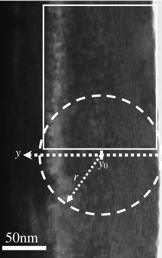
The depth-resolved EEL spectra were recorded in a
manner similar to SREELS,1) the optical configuration of
which is shown in Fig. 1: the area of interest was placed at the area subtended by a circular spectrometer aperture, with the surface edge parallel to the energy dispersion direction of a magnetic sector of the detector. A two dimensional
(positionyalong the depth direction from the surface andx
along energy lossE) spectrum image was then recorded with
an exposure of 30 s. The incident electron beam was defocused to illuminate the entrance aperture uniformly. The image intensities in the cross dispersion direction on the CCD was corrected by the electron beam intensity profile
passing through the circular aperture: for uniform
illumina-tion the electron intensity at the posiillumina-tionffiffiffiffiffiffiffiffiffiffiffiffiffiffiffiffiffiffiffiffiffiffiffiffiffiffiffiffi yis proportional to
r2 ðyy0Þ2 p
, whereris the radius of the aperture andy0
is the position of the aperture center, the y-direction being
[image:2.595.345.506.73.330.2]measured along the cross-dispersion direction, as shown in Fig. 2.
The intensity-corrected image still suffers spectrum blur-ring, not only due to the instrumental point-spread function (PSF) in the dispersion direction but also to the beam spread (defocus) by the chromatic aberration in the cross-dispersion direction. The latter, in particular, gives rise to a blurred intensity profile even at the sharp edge of the sample, because the detector entrance aperture is located slightly below the effective range of the image focal depth. Because of the high energy of electrons and the extended focal depth of TEM, the beam spread during propagating between the fluorescent screen and the detector aperture is not so significant, though a sample edge and/or a heterophase boundary are necessary to precisely make one-to-one correspondence between the depth and spectral position in the cross-dispersion direction. The above broadening effects were dramatically improved with statistical noise removed by spectrum deconvolution, using the PIXON method, its principle and practical examples of which are given in Ref. 11–13). The low-loss spectrum recorded at the same area under the same condition was used as the PSF in the dispersion direction, while in the cross-dispersion direction a gaussian PSF having the FWHM corresponding to the beam spread, estimated from the intensity broadening at the specimen edge, was used. In the actual treatment, the Pixon deconvolution first applied, followed by the intensity correction in the cross-dispersion direction. The resultant 2D spectrum images were almost free from statistical noise, each row of which reveals an EEL spectrum at the corresponding depth from the surface.
Detector
x
y
TEM image
aperture
Line-focus type
Magnetic prism
Ener
gy loss,
E
Depth-resolved EELS
Fig. 1 Schematic diagram showing optical configuration for depth-resolved EELS.
50nm
y
0y
r
Fig. 2 XTEM image of the TiO2 sample Nþ-implanted at fluence of
[image:2.595.65.271.73.362.2]2.3 Electronic structure-resolved EFTEM by multivari-ate analysis
EFTEM images were acquired with a JEOL-JEM2100F microscope operated at 200 kV equipped with a Gatan
imaging filter (GIF-TRIDIUM, 2k2k CCD). The
EF-TEM-spectrum imaging (EFTEM-SI) method applied to the
N-KELNES: 20 EFTEM images were collected by scanning
an energy slit of 2 eV a width from 380 eV to 420 eV on the energy-loss axis at the interval of 2 eV. Spatial drifts of the sample on the images were corrected by the cross-correlation method. A set of image intensities taken out of a specific point and aligned in order of energy-loss through the entire image stack represent the EEL spectrum at that position with an energy dispersion of 2 eV/channel. The pre-edge back-ground was then modeled by a power-law for the intensities between 380–390 eV, and then subtracted from the images to
obtain EFTEM images of the N-K ELNES, using the
functions on DigitalMicrographÒ.
The EEL spectrum at each position is supposed to be a linear combination of multiple ELNES features with different weights, each corresponding to a different chemical state of the implanted nitrogen and depending on the position. We hence applied a self-modeling curve resolution (SMCR) technique to decompose the set of spectral profiles into individual pure components without reference spectra. This allows us to reconstruct the SI data into separate images of the resolved components, instead of extracting the energy-filtered images of a part of the spectral features in a conventional manner. This is one of the techniques in multivariate analysis, and we adopted a fast, accurate and robust algorithm, called the modified alternating
least-squares (MALS) method.14)
3. Results
3.1 DREELS of Nþ-implanted TiO 2
Figure 2 shows a cross-sectional TEM image of the TiO2
sample implanted with the Nþfluence of31021m2(most
visible-light responsive). Defective microstructures are ob-served over the projected range of nitrogen. The bright contrast around the projected range peak would be due to preferential ion-thinning at the lower density regions con-taining the highest density of gas atoms. The relationship between the microstructures and photocatalytic response is beyond the scope of this paper and will be reported elsewhere. The depth-resolved spectrum images were then recorded with the detector entrance aperture placed just below the encircled area in Fig. 2.
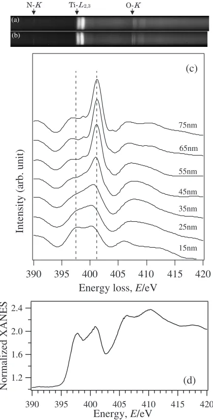
In Figs. 3(a), (b) and (c) are respectively shown as-recorded, intensity-corrected/deconvolved DREELS images recorded at 0.2 eV/channel, and the extracted depth-resolved
profiles of NK-edge ELNES. The present spatial resolution
was approximately 1 nm/row. The sample thickness of the area was found to be quite uniform and no correction for the plural scattering was taken into account.
The extracted N K-edge spectra actually exhibit clear
depth dependence, free from the statistical noise: a double-peak structure between 395 and 403 eV is seen near the surface region and a distinct single peak around 401 eV evolves with increasing the depth, which reflects different
chemical states of nitrogen, presumably depending on the local N concentration. Note that the SNR and SBR of the data are surprisingly improved, considering that the N
concen-tration around the surface region is less than 1 at%. K-edge
XANES (total electron yield mode) taken from the as-irradiated sample of the same irradiation condition is also shown in Fig. 3(d) for comparison, where the effective
electron emission depth is limited within 10nm from the
surface. The N-K XANES can also be characterized by the
double-peak structure, which well corresponds to the ELNES at the surface region in Fig. 3(c).
Detailed discussion on the chemical state corresponding to each ELNES profile observed above is not presented in this paper, but briefly the double-peak structure near the surface
could be ascribed to N replacing the O site in TiO2,7)whereas
the distinct peak around 401 eV of deeper regions would
originate from N–O and/or N–N bond formation15)possibly
2.4 2.0 1.6 1.2
Normalized XANES
420 415 410 405 400 395 390
(d)
Energy, E/eV
25nm
15nm 35nm 45nm 55nm 65nm 75nm
(c)
420 415 410 405 400 395 390
Intensity (arb. unit)
Energy loss, E/eV
(a)
(b)
N-K Ti-L2,3 O-K
Fig. 3 (a) As-recorded depth-resolved EELS image with a detector aperture inserted at the encircled area in Fig. 2. The shorter dimension corresponds to the depth direction. (b) DREELS image as a result of intensity calibration and deconvolution. See text for detail. (c) N-K
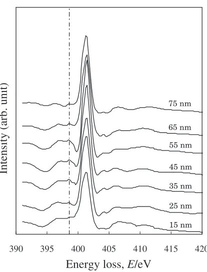
[image:3.595.323.532.73.485.2]due to the higher nitrogen concentration. A similar sharp peak at 401 eV dominates over the entire implanted regions
in the sample implanted at the fluence of 51021m2,
followed by heat-treated at 573 K (not visible-light
respon-sive), as shown in Fig. 4. N-K XANES of the same sample
(not shown) exhibited a similar single peak feature. Consid-ering that the photocatalytic reactions predominate near the surface, the visible-light responsive property should be closely related to the double-peak structure in the XANES/ ELNES.
3.2 Mapping depth distributions of different chemical states of N by multivariate analysis
Now we know that there are at least two kinds of chemical
states of N in the Nþ-implanted TiO2, we attempted
‘chemical state mapping’ by applying the SMCR technique
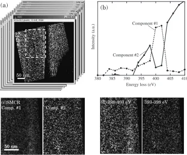
described in section 2.3. The area consisting of 100150
pixels, as framed by a solid line in Fig. 2, was used, and thus 15000 spectra could be utilized for the spectral decomposi-tion. In the present case, the number of components was assumed to be two, and two arrays of random numbers were used as the initial guess for the MALS algorithm for the pure spectra. 200 iterative least square fitting yielded a sufficiently
converged result.14)A set of 20 EFTEM images with the
pre-edge background subtracted and the resolved spectra are respectively shown in Fig. 5(a) and (b). Note that component #2 (related to visible-light responsive area) in (b) shows rather high level of post-edge background, partly because of
the multiple-loss due to the sample thickness of nearly0:8
(: mean free path for inelastic electron scattering) and partly
because of inappropriate modeling for the pre-edge back-ground. We attempted the MALS regression assuming three
components, which yielded no physically significant result. The depth distributions (SI) of the components #1 and #2 are shown in Fig. 5(c). The grayscale of each image in (c) was calibrated such that it reflects the approximate relative concentration of each component. For comparison, the EFTEM images recorded by picking up the most distinct spectral features of the two chemical states with an energy slit are also shown in Fig. 5(d). The distribution of each component is qualitatively similar to that in (c), though the concentration of #1 component is particularly too exagger-ated compared to the correct contrast in (c), because the energy slit includes significant intensities of component #2.
It should also be noted that the chemical state of component #1 (not visible-light responsive) is localized around the depth regions around 30 and 100 nm from the surface, while that of component #2 is distributed over the entire implanted regions. It is not yet clear why the single peak component shows the bimodal distribution, but
pre-sumably because the NOx and/or N2 gas molecules are
formed15) and escaped away when the N concentration
exceeds a certain value.
Since the data array of each spectrum was treated as a generalized vector and normalized by the Euclidian norm in
the MALS algorithm,14) the derived concentration of each
component does not directly stand for its chemical concen-tration. The inelastic scattering cross section for each component is hence required to evaluate the quantitative concentration of each component, which will be a next subject in our future work.
4. Summary
In the present study, depth-resolved EELS (DREELS) and chemical state mapping methods, both based on EFTEM for
XTEM samples are introduced. The techniques applied to Nþ
implanted TiO2 photocatalyst, for analyzing the electronic
states responsible for the visible-light active property. DREELS successfully extracted the depth dependence of EELS from one spatially resolved spectrum image, nearly free from statistical noise, by deconvolving the image with the Pixon method. As a result, two chemical states of nitrogen, depending on the local N concentration, were identified. The depth distributions of those chemical states were separately imaged by applying the MALS regression among an SMCR techniques to the EFTEM data set, revealing that one state relating to the visible-light response ranged over the entire implanted depth, whereas the other not visible-light responsive was localized around depths of a certain N concentration. The present method enables one to visualize the spatial distributions of specific chemical states even when the spectral profiles are overlapped. The revealed features above should be a key to solve the electronic states responsible to the visible-light catalytic activity, which is discussed elsewhere. We would like also to put an emphasis on the significance of the present methods: recent develop-ment of electron optics including the aberration correction systems has been oriented for increasing the current density of the incident electron beam and minimizing its size down to as small as sub-nanometers. This direction successfully enabled elemental mapping at an atomic resolution on one
390 395 400 405 410 415 420
75 nm
65 nm
55 nm
45 nm
35 nm
25 nm
15 nm
Energy loss,
E
/eV
Intensity (arb. unit)
Fig. 4 Depth-resolved N-KELNES of another TiO2sample (Nþ
-implant-ed at fluence of51021m2followed by heating at 573 K for 2 hours)
[image:4.595.66.273.67.339.2]hand, whereas it inevitably enhance radiation damages as a serious drawback. The methods demonstrated in the present study would solve the difficulties with little additional investment, so far as one does not require a sub-nanometer resolution. We do hope many materials scientists recognize the point and consider the methods as possible options when he or she tries to examine radiation-sensitive materials.
Acknowledgements
We are very grateful to Mrs. E. Okunishi, N. Endo and T. Oikawa at Akishima works of JEOL Ltd. for kindly conducting EFTEM-SI, essential for the present study. The present work was supported in part by a Grant-in-Aid for Scientific Research (KAKENHI) in Priority Area ‘‘Molecular Nano Dynamics’’ and ‘‘Kiban-Kenkyu A’’ from MEXT, Japan.
REFERENCES
1) K. Kimoto, T. Sekiguchi and T. Aoyama: J. Electron Microsc. 46
(1997) 369–374.
2) J. M. Martin, B. Vacher, L. Ponsonnet and V. Dupuis: Ultramicroscopy
65(1996) 229–238.
3) M. R. Hoffman, S. T. Martin, W. Choi and D. W. Bahnemann: Chem. Rev.95(1995) 69–96.
4) A. Fujisima, K. Hashimoto and T. Watanabe:Photocatalysis: Funda-mentals and Applications, (BKC Inc., Tokyo, 1999).
5) A. Fujishima, T. N. Rao and D. A. Tryk: J. Photocehm. Photobiol.C1
(2000) 1–21.
6) M. Kaneko and I. Ohkura (Eds.):Photocatalysis, (Kodansha-Springer, Tokyo, 2002).
7) R. Asahi, T. Morikawa, T. Ohwaki, K. Aoki and Y. Taga: Science293
(2001) 269–271.
8) H. Irie, Y. Watanabe and K. Hashimoto: J. Phys. Chem. B107(2003) 5483–5486.
9) Y. Nosaka, M. Matsushita, J. Nishino and A. Y. Nosaka: Sci. Tech. Adv. Mater.6(2005) 143–148.
10) http://www.srim.org/SRIM/SRIM2003.htm
11) P. K. Pina and R. C. Putter: Astr. Soc. Pac105(1993) 630–637. 12) S. Muto, R. C. Puetter and K. Tatsumi: J. Elect. Micros.55(4)(2006)
215–223.
13) S. Muto, K. Tatsumi, R. C. Puetter, T. Yoshida, Y. Yamamoto and Y. Sasano: J. Elect. Micros.55(4)(2006) 225–230.
14) J.-H. Wang, P. K. Hopke, T. M. Hancewicz and S. L. Zhang: Anal. Chim. Acta476(2003) 93–109.
15) J. Sto¨hr and R. Jaeger: Phys. Rev. B26(1982) 4111–4131.
50 nm
380 385 390 395 400 405 410
Intensity (a.u.)
Energy loss (eV) Component #1
Component #2
(a)
(b)
50 nm 50 nm (c)SMCR
Comp. #1 Comp. #2
(d) 398-403 eV 393-398 eV
[image:5.595.116.480.73.375.2]