The Effect of Strain Distribution on Abnormal Grain Growth in Cu Thin Films
Miki Moriyama
1, Kentaro Matsunaga, Toshifumi Morita
2,
Susumu Tsukimoto
2;*and Masanori Murakami
21
Optoelectronics Division, TOYODA GOSEI CO., LTD., Heiwa-cho, Nakashima, Aichi 490-1312, Japan
2Department of Materials Science and Engineering, Kyoto University, Kyoto 606-8501, Japan
The effect of intrinsic strain on grain growth in Cu thin films was studied by both plan-view and cross-sectional scanning ion microscope in a focused ion beam system. Significant grain growth with bimodal grain size distribution was observed during room temperature storage in the Cu films which were deposited on the Si3N4substrates by a sputter-deposition technique. In the thick Cu films, a non-uniform grain size
distribution was observed along a direction normal to the film surface: the large grains were observed at the location close to the substrate surface. This grain size distribution coincided with inhomogeneous strain distribution normal to the film surface. We concluded that the grain growth in the Cu thin films was facilitated by the strain intrinsic in the Cu films deposited on the rigid substrates, and that strain (or stress) introduced in the films was a primary factor to induce the grain growth in the Cu films at room temperature.
(Received June 21, 2004; Accepted August 6, 2004)
Keywords: copper films, abnormal grain growth, stress, strain
1. Introduction
Copper is attractive as interconnect materials of current Si-ULSI (Ultra-Large Scale Integrated) devices with line width of130nm. The advantages of using copper (over conven-tional Al-alloy) as the interconnect materials are lower electrical resistivity and higher reliability. However, we have concern to use the Cu interconnects in the sub-50 nm devices, because the resistivity of the Cu interconnects increased rapidly by reducing the line width.1–3) The reason was
believed to be due to the relatively long mean free path (39nm) of the conducting electrons in copper. Upon reducing the line width of the Cu interconnects down to less than 100 nm, the mean free path of the electrons in copper approaches to the line width, and the electrons scatter at the surfaces, interfaces, and/or grain boundaries, leading to drastic resistivity increase. A device designer requires the interconnect resistivity of less than 2.2m-cm to realize high-speed ULSI devices with 65 nm wide interconnects.4)In
order to realize the nano-scale Si-devices, development of ultra-narrow copper interconnects with low resistivity is essential. Our recent experimental results suggested that the grain boundary scattering increased primarily the resistivity of the Cu thin films,5)indicating that large grained films are essential for the low resistivity narrow copper interconnects. Therefore, understanding of grain growth mechanisms in the Cu thin films is extremely important to reduce the electrical resistivity of the Cu interconnects.
When the Cu films were annealed at elevated temperatures after the film deposition, a few grains grew locally at the expense of the smaller neighboring grains.6)This bi-modal
grain growth, which led to an inhomogeneous grain size distribution, was conventionally called as ‘‘abnormal grain growth’’.6) Many researchers have observed the abnormal grain growth in the Cu thin films during annealing at elevated temperature after the film deposition.7–9)In the electroplated
Cu films which are widely used in the manufacturing Si-ULSI devices, this abnormal grain growth was observed even at room temperature storage.10–17)Cabralet al.14)and Uenoet al.16)observed relaxation of stress (introduced in the
electro-plated Cu film) and grain growth simultaneously during room temperature storage. Harperet al.15)suggested that the stress change was caused by the volume change associated with elimination of grain boundaries using a grain growth model proposed by Chaudhari.18)Grosset al.11–13)and Brongersma
et al.17) suggested that organic additives added to plating
solutions which contained in the Cu films during electro-deposition might enhance grain growth in the electroplated Cu films at room temperature.
We previously reported that the room temperature grain growth occurred in the Cu films which were prepared by a sputtering technique, and concluded that the organic addi-tives (needed in electroplating) are not only the primary factor for the Cu grain growth. Since Cu films have intrinsic strain when deposited on the rigid substrates, the strain introduced in individual grains of the Cu film was concluded to be the primary factor to induce the abnormal grain growth.19)Strain in the metal films is generally induced from the rigid substrate and strain distribution would not be uniform. This non-uniform strain was observed for blanket Pb films in a direction normal to the substrate surface.20)
Thus, if the strain is the primary factor for grain growth at room temperature, the grain growth in the Cu films would be effected by the strain gradient and that the grain growth rates are different in direction normal to the substrate surface. This growth mechanism may explain the abnormal grain growth mechanism observed parallel to the film surface.
The primary purpose of the present experiment was to study the effect of the strain distribution in a direction normal to the substrate surface on the grain growth, and to under-stand the abnormal grain growth mechanism in the Cu thin films. We deposited relatively thick Cu films with various thicknesses (100nm6mm) on the rigid substrate by the sputter-deposition technique. The microstructures were an-alyzed by focused ion beam (FIB) spectroscopy in both plan-*Corresponding author,
views and cross-sectional. These studies will provide us a guideline for developing the low resistance Cu films with large grain size.
2. Experimental Procedures
(100)-oriented Si wafers, which were coated with chemi-cal-vapor deposited (CVD) Si3N4, were used as the sub-strates. Prior to sputter-deposition, the substrates were ultrasonically cleaned with acetone and IPA (isopropyl alcohol) for 3 min/each. After blowing with dry N2gas, the substrates were mounted on the sample holder and immedi-ately loaded into the load-lock chamber of the radio-frequency (RF) magnetron sputtering system. The substrates were transferred to the deposition chamber with the base pressure of about1106Pa through the load-lock cham-ber. The Cu films with thicknesses ranging from 100 nm to 6mm were deposited by RF sputtering onto the Si3N4 substrates which were cooled by water during deposition. The working pressure during the deposition was about 5 101Pa. The samples were annealed isothermally at room temperature in air. Microstructural analysis of the Cu films was carried out by scanning ion microscope (SIM) in the focused ion beam (FIB) system. SIM observations were performed in both plan-views and cross-sectional. For the cross-sectional SIM observations, the samples were milled by the FIB system. The electrical resistances in the Cu films were measured by a four-point probe method.
3. Experimental Results
3.1 Cu films with 100 nm thick
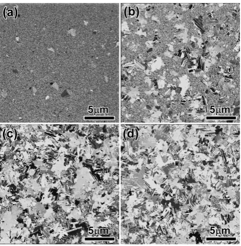
Figures 1(a)–(d) show the plan-view scanning ion micro-scope (SIM) images of the 100 nm-thick Cu film deposited on
the Si/Si3N4 substrate after storing at room temperature for 4 h, 6 h, 9 h and 16.5 h, respectively. As shown in Fig. 1(a), the as-deposited Cu films are found to have both large and fine grains. The sizes of the most grains are extremely small (<20nm), and are about one-fifth of the film thickness. However, large grains in the range of 100 nm to 1mmin size are locally observed. As the storage time increases, the large grains grow at the expense of the small grains and the fraction of the fine-grained area decreases as seen in Figs. 1(a)–(d). These large grains continue to grow while the surrounding small grains are stable. This bi-modal grain growth rate leads to an inhomogeneous grain size distribution in a direction parallel to the film surface. The present result clearly demonstrated that the room temperature grain growth, which has been previously reported for the electroplated Cu films,10–17)also occurred extensively in the sputter-deposited Cu thin film, which do not contain additives (added to the plating solutions). Thus, the additives (added in the electro-plated Cu films) are not only the primary factor to induce room temperature grain growth in the Cu films.
Figure 2 shows changes of (111) XRD peak profiles of the 100 nm-thick Cu film deposited on the Si/Si3N4 substrate during room temperature storage. The (111) peak intensities increase during room temperature storage, while the half-widths of the (111) diffraction peaks decrease. These results indicate that the (111) oriented grains in the Cu film grow during room temperature storage.
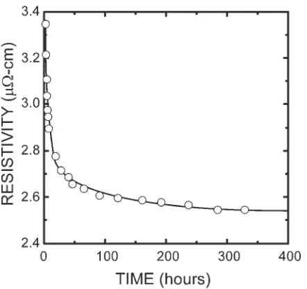
Figure 3 shows changes of electrical resistivities () of the 100 nm-thick Cu film during room temperature storage. The resistivity of the as-deposited Cu film is 3.35m-cm, which is about two times larger than the value of the bulk Cu (1.67m-cm). The resistivity drastically decreases at the
Fig. 1 Plan-view SIM images of the 100 nm-thick Cu film deposited by sputtering on the Si/Si3N4substrate, and annealed at room temperature for
(a) 4 h, (b) 6 h, (c) 9 h, and (d) 16.5 h.
Fig. 2 Changes of (111) XRD peak profiles of the 100 nm-thick Cu film deposited by sputtering on the Si/Si3N4substrate, and annealed at room
temperature.
[image:2.595.49.290.503.749.2]initial stages of the room temperature storage. The rate of the resistivity decrease becomes extremely slow after 100 h. The value is 3.0m-cm at 5 hours after the deposition, decreases over a period of 300 hours, and reaches a value of about 2.55m-cm. Considering the results shown in Figs. 1 and 2, the reduction of thevalues is explained by the reduction of the grain boundary density in the film due to grain growth as observed previously.19)
3.2 Cu films with large thickness
Figures 4(a)–(f) are the plan-view SIM images of the Cu films with the thickness of 1mmdeposited on the Si/Si3N4 substrate after storing at room temperature for 4 h, 7 h, 10 h, 12 h, 15 h and 21.5 h, respectively. The grain growth behavior of the 1mm-thick Cu film is similar to that observed in the 100 nm-thick Cu film shown in Fig. 1. However, the grain growth rate of the 1mm-thick Cu film is slower than that of the 100 nm-thick Cu film. As shown in Fig. 4(a), a homoge-neous grain size distribution is observed and the average grain size is quite small (20nm) in the film after 4 hours storage. This homogeneous size distribution was not ob-served in the 100 nm-thick Cu film of Fig. 1(a). Although a fraction of the fine-grained area decreases as the storage time increases, about 25% of the total area is covered with the fine-grained area even after 21.5 hours storage as shown in Fig. 4(f).
Figure 5 shows changes of (111) XRD peak profiles of the 1mm-thick Cu film deposited on a Si/Si3N4substrate during room temperature storage. The peak intensities increase during room temperature storage, indicating that the (111) oriented grains grow during room temperature storage.
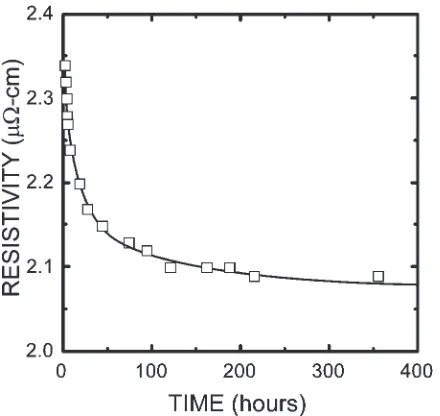
Figure 6 shows changes of electrical resistivities () of the 1mm-thick Cu film during room temperature storage. The resistivity decreases with increasing storage time similar to the behavior observed in the 100 nm-thick Cu film. However, the resistivity of the as-deposited 1mm-thick Cu film is 2.35m-cm which is smaller than the value of the
as-deposited 100 nm-thick Cu film, albeit the average grain size of the 100 nm-thick Cu film is larger. The present exper-imental results shown in Figs. 5 and 6 suggest that the grain size of the as-deposited 1mm-thick Cu film is not uniform along a direction vertical to the film surface and that grains close to the Si3N4substrate would have larger sizes.
In order to investigate the microstructure of the Cu films vertical to the film surface, cross-sectional SIM observation was carried out. Figures 7(a)–(f) show cross-sectional SIM images of the 1mm-thick Cu film after storage at room temperature for various times. As shown in Fig. 7(a), the 1mm-thick Cu film stored for 4 hours at room temperature after deposition is composed of two layers: large grains at a location close to the substrate surface (0:30:6mmfrom the bottom), and small grains close to the film surface (<20nm from the top). The thickness of the large grained layer is about 0.4mm. After 46 hours storage at room temperature, these large grains at the bottom of the film grow toward the film surface at the expense of the fine grains in the top layer. Such the abnormal grain growth which initiated from the film/substrate interface was clearly observed in a 6mm-thick Cu film (Fig. 8). After 7 hours storage at room temperature, the thickness of the large grained layer is about 1mmfrom the bottom (Fig. 8(a)). During storage at room temperature, the
Fig. 3 Changes of electrical resistivities () of the 100 nm-thick Cu film deposited by sputtering on the Si/Si3N4substrate, and annealed at room
temperature.
Fig. 4 Plan-view SIM images of the 1mm-thick Cu film deposited by sputtering on the Si/Si3N4substrate, and annealed at room temperature for
[image:3.595.60.281.69.277.2]large grains at the bottom grow at the expense of the small grains at the top layer. The thickness of the large grained layer at the bottom increases to about 3mmafter 33 hours storage (Fig. 8(c)). This abnormal grain growth at room temperature continues over a period of 60 days (Figs. 8(a)– (e)). Note that the average thickness of the large grained layer is about 4mmand some large grains reach at the film surface, while the small grains at the top of the film are stable (Fig. 8(e)).
4. Discussion
4.1 Effect of horizontal strain distribution on the abnormal grain growth in Cu thin films
As shown in Figs. 1 and 4, the as-deposited Cu films were found to have the very fine grains (<20nm). The films with fine-grains are thermodynamically unstable since the films have a high density of grain boundaries with large grain boundary energy. This large grain boundary energy provides a ‘‘macroscopic’’ driving force for grain growth. Grain growth takes place to reduce the grain boundary energy if sufficient thermal energy is given to migrate the grain boundaries.
We previously reported that significant grain growth occurred during room temperature storage in the sputtered Cu films deposited on the rigid substrates, and that no grain growth occurred during room temperature storage in the free-standing Cu films.19) The previous experimental results suggested that the grain growth in the Cu films did not occur at room temperature unless additional energetic assistance to enhance grain boundary migration was given to the films.
In general, intrinsic strains (or stresses) are observed in metal films deposited on rigid substrates.20) The intrinsic
stress in the sputter-deposited Cu films is of the order of 10–
102MPa.21,22) The intrinsic strains could provide such the
energetic assistance to the room temperature grain growth in the Cu films bonded to the rigid substrates. If the strain exceeds the yield stress of the film, the strain in the film will be relaxed by several deformation (or strain relaxation) mechanisms which may operate simultaneously, and the strain relaxation mechanisms have dependence on the film microstructure.23)The stored energy of each grain after strain relaxation has also dependence on the film microstructure,
Fig. 5 Changes of (111) XRD peak profiles of the 1mm-thick Cu film deposited by sputtering on the Si/Si3N4substrate, and annealed at room
temperature.
Fig. 6 Changes of electrical resistivities () of the 1mm-thick Cu film deposited by sputtering on the Si/Si3N4substrate, and annealed at room
temperature.
Fig. 7 Cross-sectional SIM images of the 1mm-thick Cu film deposited by sputtering on the Si/Si3N4substrate, and annealed at room temperature for
[image:4.595.89.248.71.332.2] [image:4.595.306.547.73.327.2] [image:4.595.60.280.401.609.2]and such complex deformation processes will lead to wide energy distribution.23) For a polycrystalline film in which
grains have various sizes and crystal orientations, the strain energy stored in each grain depends on both the grain size or crystal orientation.23)Since Cu has strong anisotropy in the
elastic constants, an inhomogeneous elastic strain energy distribution is introduced in the film. We strongly believe that this wide energy distribution among grains of the Cu film would induce abnormal grain growth in Cu films.
4.2 Effect of vertical strain distribution on the abnormal grain growth in Cu films
A vertical non-uniform grain size distribution in the Cu film observed in Figs. 7 and 8 would be due to a non-uniform vertical strain distribution in the Cu film. Strain and stress in metal films are generally introduced from the rigid substrate
and non-uniform strain distribution was observed for blanket films in direction normal to the substrate surface.24) An
exponential thermal strain distribution normal to the film surface was experimentally determined for Pb thin films using X-ray line broadening analysis.24) An empirical
exponential strain distribution given by,
"mðhmÞ ¼"nexp hhm
where"nis the strain at the film/substrate interface,"mis the
average strain in a small volume element at a distance (hm)
[image:5.595.55.279.66.527.2]from the film surface, and1=is a proportionality constant. This strain distribution is indicated by arrows shown in Fig. 9.
The large strain close to the substrate enhances the growth of the grains located close to the substrate (the bottom of the film). As the film thickness increases, the influence of the strain introduced to the film from the interface becomes weak, and the top layer approaches to the properties of the free-standing film (or the bulk materials). The strain close to the top surface of the thick film is almost relaxed to zero. Therefore, as the film thickness increases, the grain growth rate close to the top surface becomes extremely slow as observed previously in the free-standing films.19)The grains which grow very quickly from the bottom to the top surface figure the large grains when observed from the top view and vice versa. This growth mechanism also results in abnormal
Fig. 8 Cross-sectional SIM images of the 6mm-thick Cu film deposited by sputtering on the Si/Si3N4substrate, and annealed at room temperature for
(a) 7 h, (b) 19 h, (c) 33 h, (d) 332 h, and (e) 60 days.
[image:5.595.306.550.70.410.2]grain growth when the observation is made on the film surface. The present results indicate that the non-uniform strain (or stress) distribution in the film causes wide grain size distribution normal to the Cu film surface, and that strain introduced from the substrate and strain relaxation mecha-nisms are the key factors to control the grain growth in the Cu films. Therefore, the properties of the interface between the substrates (or the barrier layers) and the Cu films have an important role to control grain growth behaviors in the Cu films.
5. Summary
Microstructures of the sputtered Cu films were analyzed by both plan-view and cross-sectional scanning ion microscope in a focused ion beam system. Significant grain growth (with bimodal grain size distribution) was observed during room temperature storage in the Cu films deposited on the Si3N4 substrates. When the film thickness was greater than 1mm, room temperature grain growth occurred close to the film/ substrate interface, while the grains close to the top of the film were stable. The present results suggested that the grain growth kinetics in the Cu films were strongly influenced by the existence of the rigid substrates, indicating strain (or stress) introduced in the films was a primary factor to induce the grain growth in the Cu films.
Acknowledgements
This work was partially supported by a grant-in-aid for Scientific Research from the Ministry of Education (No. 15206069).
REFERENCES
1) K. Fuchs: Proc. Camb. Phil. Soc.34(1938) 100. 2) E. H. Sondheimer: Adv. Phys.1(1952) 1.
3) A. F. Mayadas and M. Shatzkes: Phys. Rev.B1(1970) 1382. 4) ITRS roadmap for 2003.
5) M. Moriyama, M. Shimada, H. Masuda and M. Murakami: Trans.
Mater. Res. Soc. Jpn.29(2004) 51–54. 6) C. S. Smith: Trans AIME188(1950) 1021.
7) E. M. Zielinski, R. P. Vinci and J. C. Bravman: J. Appl. Phys.76(1994) 4516.
8) D. P. Tracy and D. B. Knorr: J. Electronic Mater.22(1993) 611. 9) D. A. Smith, S. J. Townsend and C. S. Nichols: Mat. Res. Soc. Symp.
Proc.238(1992) 531.
10) T. Ritzdorf, L. Graham, S. Jin, C. Mu and D. B. Fraser:Proceedings of the International Interconnect Technology Conference, (IEEE, New York, 1998) p. 166.
11) M. E. Gross, K. Takahashi, C. Lingk, T. Ritzdorf and K. Gibbons:Adv. Metallization Conf. 1998, ed. by G. S. Sandhu, H. Ko-erner, M. Murakami, Y. Yasuda and N. Kobayashi (Mater. Res. Soc., Pittsburgh, PA, 1999) p. 51.
12) C. Lingk and M. E. Gross: J. Appl. Phys.84(1998) 5547.
13) C. Lingk, M. E. Gross, W. L. Brown, W. Y.-C. Lai, J. F. Miner, T. Ritzdorf, J. Turner, K. Gibbons, E. Klawuhn, G. Wu and F. Zhang:Adv. Metallization Conf. 1998, ed. by G. S. Sandhu, H. Koerner, M. Murakami, Y. Yasuda and N. Kobayashi (Mater. Res. Soc., Pittsburgh, PA, 1999) p. 89.
14) C. Cabral, Jr., P. C. Andricacos, L. Gignac, I. C. Noyan, K. P. Rodbell, T. M. Shaw, R. Rosenberg, J. M. E. Harper, P. W. DeHaven, P. S. Locke, S. Malhotra, C. Uzoh and S. J. Klepeis:Adv. Metallization Conf. 1998, ed. by G. S. Sandhu, H. Koerner, M. Murakami, Y. Yasuda and N. Kobayashi (Mater. Res. Soc., Pittsburgh, PA, 1999) p. 81. 15) J. M. E. Harper, C. Cabral, Jr., P. C. Andricacos, L. Gignac, I. C.
Noyan, K. P. Rodbell and C. K. Hu: J. Appl. Phys.86(1999) 2516. 16) K. Ueno, T. Ritzdorf and S. Grace:Adv. Metallization Conf. 1998, ed.
by G. S. Sandhu, H. Ko-erner, M. Murakami, Y. Yasuda and N. Kobayashi (Mater. Res. Soc., Pittsburgh, PA, 1999) p. 95.
17) S. H. Brongersma, E. Richard, I. Vervoot, H. Bender, W. Vandervorst, S. Lagrange, G. Beyer and K. Maex: J. Appl. Phys.86(1999) 3642. 18) P. Chaudhari: J. Vac. Sci. Technol.9(1972) 520.
19) M. Moriyama, K. Matsunaga and M. Murakami: J. Electron. Mater.32
No. 4 (2003) 261–267.
20) K. L. Chopra: Thin Film Phenomena, (McGraw–Hill, New York, 1969).
21) A. Entenberg, V. Lindberg, K. Fletcher, A. Gatesman and R. S. Horwath: J. Vac. Sci. Technol.A5(1987) 3373–3377.
22) A. F. Burnett and J. M. Cech: J. Vac. Sci. Technol.A11(1993) 2970– 2974.
23) M. Murakami, T.-S. Kuan and I. A. Blech:Mechanical Properties of Thin Films on SubstratesinTREATISE ON MATERIALS SCIENCE AND TECHNOLOGY, ed. by K. N. Tu and R. Rosenberg, (Academic press, New York, 1982).