Abstract—A quantitative analysis of the dielectric properties of a multiphase sample using a Scanning Microwave Microscope is proposed. The method is demonstrated using inhomogeneous samples composed of a resin containing micrometric inclusions of a known ceramic material. The Scanning Microwave Microscope suitable for this task employs relatively large tips (tens of micrometers in diameter). Additionally, in order to make the instrument more suitable for high-throughput analysis, an original design for rapid tip changes is implemented. Single-point measurements of dielectric constant at random locations on the sample were performed, leading to histograms of dielectric constant values. These are related to the dielectric constants of the two phases using Maxwell-Garnett effective medium theory, taking into account of the volume-of-interaction in the sample beneath the tip.
Index Terms— Dielectric constant, Dielectric materials, Maxwell-Garnett Approximation, Microwave measurements, Near-field measurements, Nonhomogeneous media, Statistical Distributions, Scanning Microwave Microscopy.
I. INTRODUCTION
he analysis of the dielectric properties of multiphase materials is important in many scientific fields [1]. The near-field Scanning Microwave Microscope (SMM) has been extensively exploited to this purpose [1] even though the problem of modeling the tip-sample interaction is still an open research topic [2],[3].
Many implementations of the SMM are based on atomic-force microscope platforms, using non-contact interaction with very fine (nm scale) tips [4]. Such approaches are not suitable for rough surfaces or large samples where the features of interest may be many tens of micrometers in extent. In this case coarser movements and larger tips are appropriate. If considering, for example, circuits and integrated devices for power electronics, the single elements and connections are usually several hundreds of micrometers in size [5]. These features are still too small to be efficiently tested by a conventional miniaturized dielectric probe [6]. A similar situation is found in other applications, ranging from the
high-T. Monti, O. B. Udoudo, C. Dodds, S. W. Kingman are with the Faculty of Engineering, University of Nottingham, NG7 2RD Nottingham UK (e-mail: [email protected]; [email protected]; [email protected]; [email protected]).
K. Sperin and T. J. Jackson are with the School of Engineering, University of Birmingham, B15 2TT Birmingham UK (e-mail: [email protected]; [email protected]).
power microwave processing of materials [7], where the dielectric features of micrometric inclusions in the treated materials strongly influence the treatment efficiency itself [8], to the diagnosis of 3D-printed circuit elements [9], especially when assembled in a complex board. Engineering applications like these, usually involve natural or man-made multiphase materials at micrometric scale with uncontrolled roughness and partially known composition. So far the SMM has hardly been used to study such materials, even though potential benefits, such as fault detections and process quality assessments, can come from dielectric analysis.
Additionally, in realistic contexts, such as in situ high-throughput diagnostic processes, a full scan of the object under analysis is not required, and would be extremely time-consuming. A statistical description of the dielectric properties is much more suitable, provided some a priori information about the materials under analysis. This can be applied in the case of a production chain where the location of the assembled components is known and defects can be identified by the variations from the known topology.
The ability to rapidly change tips is essential to such application of SMM. Furthermore, in such cases, a semi-empirical approach for calibration is pragmatic to use. Such a calibration provides validation of the instrument, it does not require detailed knowledge of the geometry of the tip and it yields simply-derived estimates of the error bars.
In this work a bespoke SMM with the features described above (tips of tens of micrometers size, agile system for changing tips, etc.) is applied to the dielectric characterization of a set of exemplar two-phase samples. A statistical strategy is adopted for a comprehensive description of the samples’ dielectric properties. Rather than collecting sample images, the SMM dielectric measurements are taken as single-points at locations chosen randomly. The dielectric permittivity results are related to the distribution of one phase with respect to the other by considering the Maxwell-Garnett approximation for the effective medium included in the SMM volume of interaction [10]. Such volume extends in all three planes defined by x, y and z. The SMM probe is insensitive to the material properties outside this volume. Due to the random nature of the SMM measurements the composition of the portion of the sample under analysis is not known. In order to confirm the validity of the effective medium approximation, the samples are subsequently analyzed by the Scanning Electron Microscope – Extended Back-Scattering Electron
Statistical Description of Inhomogeneous
Samples by Scanning Microwave Microscopy
Tamara Monti, Ofonime B. Udoudo, Kevin A. Sperin, Chris Dodds, Sam W. Kingman, Timothy J.
Jackson
(SEM-XBSE) technique interpreted by the Mineral Liberation Analysis (MLA) software. The MLA provides an automated scan of the sample surface with pattern matching of the x-rays collected in a database. The software is used to build an image from which particle parameters, including dimensions, are calculated. This analysis is necessary in the current work in order to precisely determine the area of the inclusions (first phase) and the ratio of these with respect to the host medium (second phase).
The theoretical methods used to evaluate the performance of the SMM and analyze the data are presented in section II. Section III details the experimental procedures. The results are presented and discussed in Sections IV and V, respectively. The novel features of this work are the determination of the lower bounds of dielectric loss that can be resolved by such an SMM (Sec. IV.A), the statistical treatment of two-phase samples with independent characterization of physical properties (Sec. IV.C), the consideration of the volume of interaction beneath the SMM tip and, from the design point of view, the SMM head that enables a rapid interchange of probe tips (Sec. III).
The final aim of the paper is to widen the application of the SMM to new areas where it is important to have high-throughput dielectric information of relatively large samples and with micrometric inclusions. The practical novelties of the proposed design and the statistical approach (Sec. III), instead of full scans of the samples, make the proposed instrument suitable for the latter purpose. The semi-empirical model used for deriving the dielectric constant from the microwave measurements, described in Sec. II, makes the technique accessible outside the microwave community as well.
II. THEORY
In most cavity resonator SMMs, including the one used in this work, a sharp tip protrudes through the aperture from the center conductor. This is commonly modelled as a capacitance
t
C connected in parallel with the resonator capacitance C. A sample beneath the tip is modelled by an additional impedance [11-13] related to the sample’s complex relative permittivity
2
1
j . The sample may be considered “low loss” if its loss tangent tan
2
1QL, where QL is the loaded quality factor of the resonator, because in this case the resonator will be insensitive to dissipation in the sample. Such a sample presents only an additional capacitance Cs in series with Ct. The resonance frequency of the probe will fall from f0without the sample to a lower value f with the sample. This is expressed as a normalized frequency shift of
t s
s t C C C C C f f 2 1 0 (1)
when the shift is small. (1) is an equation which needs a model for Csas a function of sample permittivity to be really useful. Alternative estimates of the frequency shift [14], [15] have been obtained by calculation of the electric field around spherical [14] and axisymmetric [15] tips using an image
charge analysis. The frequency shift was calculated using perturbation theory in the spherical case to be
1 1 ln 0 b b A f f f f (2),with 𝑏 = (𝜀1− 1)/(𝜀1+ 1). An alternative empirical expression has also been proposed [16]
1 1 1
f f (3).In this model, and are constants principally related to the distribution of electric fields around the tip and the size of the aperture, respectively. All three models are based on the assumption that the current distribution within the resonator is not changed by the sample. Both (2) and (3) can be arranged in a linear form, yielding gradient and intercept terms which become the calibration constants. The x-ordinate data should be taken with respect to the mean value in order to remove the correlation and covariance between the gradient and intercepts [17].
Once the calibration data have been obtained, yielding gradient mand intercept c, frequency shift data from an unknown sample can be converted to relative permittivity via an inversion. For the Inoue model (3), the appropriate equation is
f f
m f f c m 1 1 1 1
(4)
where 1 is the mean value of 1 in the calibration set. The errors in the calibration data can be estimated by assuming the model to be a good description of the data and computing the standard deviation
required to make
1
2
2
i
i i f f
y
(5).
The errors in the gradient and intercept parameters can be calculated using the value of
deduced from 2 2 1 2 1
Nm (6)
and 2 2 1 2 1 2 1 N
c (7)
whereNis the number of samples in the set. The error terms in (6) and (7) may be used to calculate the error bars for the extracted relative permittivity 1. Since the gradient mand intercept care independent, (8) can be used to derive the experimental error in the determination of 1,
2 2 1 2 2 1
1 m dc c
d dm
d
(8).
the effective medium interacting with the tip is [18], [19] 𝜀1𝑒𝑓𝑓= 𝜀1ℎ+ 3𝑉𝜀1
ℎ
𝜀1𝑖 +2𝜀1ℎ 𝜀1𝑖 −𝜀1ℎ−𝑉
(9),
where 𝜀1𝑒𝑓𝑓, 𝜀1ℎ and 𝜀1𝑖 are the relative dielectric permittivity of the effective medium, the host medium and of the inclusions, respectively. 𝑉 is the volume fraction filled by the inclusions within the total volume of interaction. The Maxwell-Garnett approximation requires that the working regime is ‘quasi-static’, which is reasonable here because of the near-field interaction due to the proximity of the probe and sample [19]. It is assumed that the inclusions are physically separated. The limited volume of interaction with respect to the size of the inclusions ensures that the effect of the particle shape is not relevant [18].
In order to model the random variability of the interacting volume between tip and sample for each measurement, 𝑉 was considered as a statistical variable with Gaussian distribution 𝑓(𝑥) with a certain mean value 𝜇 and standard deviation 𝜎:
𝑓(𝑥|𝜇, 𝜎2) = 1 𝜎√2𝜋𝑒
−(𝑥−𝜇)22𝜎2 (10).
The 𝜇 and 𝜎 parameters depend on sample composition and particles distribution. This assumption is based on the sample preparation procedure, described in the next section.
III. EXPERIMENTAL METHODS
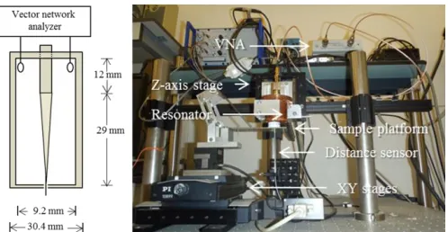
The full SMM set-up is shown in Fig. 1. A schematic of the SMM resonator is presented in the left part of the figure. Such configuration is inspired by the seminal work of Wei, et al. [20] and employed in [1], [14], [16]. The SMM used here is based on one reported elsewhere [21], adapted for high-throughput.
The top of the center conductor is threaded. The center conductor is fixed to the top-plate from inside the body of the resonator by screwing the threaded end through a tapped hole in the center of the top-plate. The center conductor is pre-loaded with a tip before insertion. This system allows for the rapid change of the tip in case of damage during the scan. Fig. 2 shows the bottom of the SMM resonator. The bottom plate comprises of two, semi-circular 3D-printed plastic discs, covered with copper tape. The two halves can be closed from the sides rather than from above the tip, thus avoiding possible damage.
Scattering parameters were recorded using a frequency-swept signal from a vector network analyzer (Copper Mountain Technologies TR5048). The VNA was typically set to an IF bandwidth of 300 Hz and to record 201 data points over six resonance bandwidths, giving a frequency resolution of the order of 50 kHz. This is considerably larger than the frequency setting resolution of the instrument, which is 10 Hz. Sweeps were averaged with an averaging factor of ten. The resonant frequency and quality factor were extracted by fitting to the data sets as described elsewhere [22], [23].
To maintain the samples in contact with the tip, a spring-loaded cantilever platform was used as a sample stage. Below the plate an infra-red distance sensor [Philtec Inc, D63-L] was used to measure the deflection and vibration of the plate, as in [24]. The resonator was lowered towards the sample until the vibrations of the plate just stopped. A maximum contact force of 20 N was deduced from the deflection of the plate.
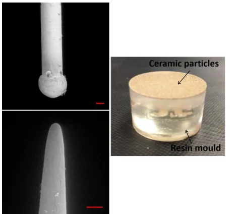
[image:3.612.314.563.48.177.2]Two tips were used for measurement of the samples, a 180 m diameter spherical tungsten tip on a 500 m diameter shaft [25] and a sharp gold-plated tungsten tip of nominal final diameter 20 m [PSPTG20100 from Tech-Specialities Inc., Sandia, USA] (Fig. 3). The larger tip was found to be robust, so calibration measurements were taken during the start and end of measurements with that tip and the final mean calibration was applied to the data. The differences in the two calibrations compared with the mean were of the order of 1% in the gradient term and 0.5% in the intercept term. Variations between data sets for the 20 μm tip were observed to be larger so this tip was calibrated before measurements of each sample. Analysis of the six individual calibrations compared with their mean showed a maximum-to-minimum variation of 25% in the gradient term and 14% in the intercept term, with no systematic trend between data sets.
Fig. 1. The scanning microwave microscope. Samples are placed beneath the resonator on a spring-loaded cantilever platform. Deflection of the platform as the resonator is lowered into contact with the sample is recorded with a distance sensor located beneath the platform. The sample may be scanned by means of the motorized stages shown. Sample movements are preformed out of contact with the resonator. On the left side, schematic of the quarter-wavelength co-axial resonator.
[image:3.612.315.557.248.408.2]Calibrations of the resonator were performed with a set of standard samples detailed in [21], [26], [27]. All were characterized in a split post resonator [21], [26], except the quartz and LaAlO3 for which standard values were assumed
[27]. The temperature variations in the laboratory during experimental runs were monitored to be of the order of ±10C.
The coefficient of thermal expansion of copper is 17 ppm -1
[28].
The dielectric materials were chosen in order to present a wide range of dielectric contrast between inclusions and hosting medium. The materials chosen for three samples were: 1) BZT (Barium Zirconate Titanate) with 𝜀1≈ 29.5 and
Q factor of 40-50000 at 1.8 GHz;
2)
CTNA (Calcium Titanate NeodymiumAluminate/CaTiO3–NdAlO3) with 𝜀1≈ 45 and Q factor of 25000 at 2 GHz;
3)
BNT (Barium Neodymium Titanate/BaNd2Ti4O12 with𝜀1≈ 80 and Q factor of 5000 at 2 GHz.
These dielectrics are commonly employed in dielectric resonators and they were manufactured and characterized by Filtronic Comtek (http://www.filtronic.com/).
Each of the three samples was made by crushing a block of dielectric material and sieving the particle fragments to control their mean size (~250 μm) [class size -300+212]. The particles were embedded in epoxy resin in 25 mm cylindrical moulds and left to cure overnight. The cured sample was then polished down to ~1 μm roughness (see Fig. 3). The dielectric permittivity of the epoxy was characterized by SMM and also by an open-ended coaxial probe technique [29].
Each sample was examined with the SMM. A first set of measurements with the 180 μm tip was performed, and the permittivity data extracted from the resonant frequency according to the procedure described previously. Between measurements the resonator was raised and the sample moved to a new position selected by a random number generator. This method was chosen to avoid any bias during the test. More than 50 SMM measurements were taken for each sample. The procedure was then repeated for the 20 μm tip. A distribution of dielectric constant values was obtained from each set of measurements.
Since the sample is composed of two solid phases (epoxy and dielectric), the volume fraction filled by each one was unknown a priori. Therefore, in order to further characterize the samples under study, a surface analysis was made using the Extended Backscattered Electron (XBSE) technique in a FEI Quanta 600i Scanning Electron Microscope (SEM). Quantitative data on the number of dielectric particles embedded in resin host, the area of each particle, and the surface occupied by them with respect to the total sample surface was obtained through use of Mineral Liberation Analysis (MLA) software. The volume of the sample probed by the backscattered electrons is of the order of a few tenths of a micrometers in diameter [30], so the MLA data are surface specific compared with the SMM data where the interaction volume is expected to be determined largely by the diameter of the tip.
IV. RESULTS A. One port calibration of the resonator
Fig. 4 shows the magnitude of S11(f)for the closed resonator, the resonator with the aperture in the base plate and the resonator with the 20 m tip protruding through the aperture. Values ofS11
f0 , f0 and QLwere determined from fitting the theoretical model described in [22] to the data. Table I shows the equivalent circuit parameters determined from the data. Fig. 4 and Table I show that the reactance of the resonator is strongly perturbed by the addition of the tip but that the aperture required for the tip itself presents only a very small perturbation. This explains the very high quality factor in the resonator used in [16], which had no tip. The tip itself presents little dissipation. However the quality factor is clearly too low compared to the quality factor of both the sample calibration set and the dielectric samples under test to be able to resolve their dielectric losses. For this reason, dielectric loss will not be considered further in this paper.
Fig. 3. On the left, SEM pictures of the tips before mounting on the resonator. Scale bars represent 50 μm. On the right, picture of the sample.
[image:4.612.324.562.48.260.2] [image:4.612.327.563.534.696.2]
TABLEI
EQUIVALENT CIRCUIT PARAMETERS
Resonator 2 1
n R() L(nH) C(fF)
Closed 0.67 1.34 251 26.5
With aperture 0.67 1.35 250 26.6
With tip 0.67 1.36 146 61.4
Equivalent circuit parameters determined from one port characterization of the resonator. The tip used was the 20 m tip. The unloaded quality factors are 2294, 2271 and 1131 for the closed resonator, resonator with aperture and resonator with tip, respectively.
B. Two port calibration of the SMM
In all that follows, the data shown are from magnitude and phase measurements of S21 taken after a full two-port calibration. The coupling was much weaker than for the one-port measurements in order to make 𝑆21≤ −20 dB. The reference planes were at the connection to the resonator coupling ports.
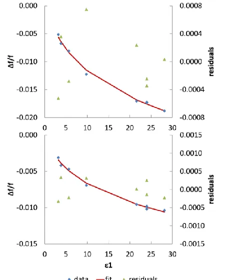
Fig. 5 shows an example of normalized frequency shift obtained from the calibration sample set for the 180 m tip and for the 20 m tip by applying the image charge model (2) to the data. The corresponding fitting parameters are given in Table II.The same data are shown in case of Inoue’s model (3) in Fig. 6 and Table III.
The fractional errors for the two models are very similar in magnitude: the data for the image charge model are consistent with an analysis reported previously on the measurement of thin films [21]. However in most cases the Inoue model (3) gave slightly lower errors than the Gao-Xiang model (2). The fractional standard errors shown in Table III are approximately 7% in the gradient and 3% in the intercept for both tips. The Inoue model is the more convenient one of the two for the analysis that follows because it provides a linear equation for extraction of an unknown permittivity from a measured frequency shift and hence it leads to a simpler estimation of the uncertainty in the extracted permittivity. For normalized frequency shifts of -0.015 (180 μm tip) and -0.008 (20 μm tip) in the calibration data, the uncertainty in the extracted permittivity 𝜎𝜀1 is approximately 1, or 10% of the true relative permittivity.
In order to assess the success of the calibration, an epoxy sample was tested by SMM and by an open-ended coaxial probe technique [29]. The dielectric permittivity of the epoxy as characterized by SMM was 𝜀1ℎ= 3.2 with a 6% standard deviation over five single-point SMM measurements on different spatial locations. The error is likely to be related to intrinsic variations of the epoxy sample. The value obtained by the open-ended coaxial probe technique was 𝜀1ℎ= 3.1.
Temperature drift in the laboratory during measurements could have caused drift in the measured resonant frequencies of 17.6 ppm, or about 30 kHz. For the MgO sample of permittivity 9.8, the frequency shifts were typically 12250 ppm for the 180 m tip and 7370 ppm for the 20 m tip respectively. The error in resonant frequency introduced by temperature drift for MgO was less than 0.25%.
TABLEII
FITTING PARAMETERS –GAO-XIANG MODEL
Tip m
m
c
[image:5.612.328.562.50.330.2]c 180 m 0.009015 0.000703 -0.012840 0.000401 20 m 0.004915 0.000438 -0.007355 0.000250 Typical fitting parameters from calibration data for the Gao-Xiang image charge model (2).
Fig. 5. Final mean calibration data in case of 180 μm tip (top) and 20 μm tip (bottom) for the Gao-Xiang image charge model (2).
[image:5.612.309.565.350.707.2]TABLEIII
FITTING PARAMETERS –INOUE MODEL
Tip m
m
c
c
180 m 41.97 2.817 931.4 27.39
20 m 76.45 5.526 1628 53.74
Typical fitting parameters from calibration data for the Inoue model (3).
C. Statistical Description
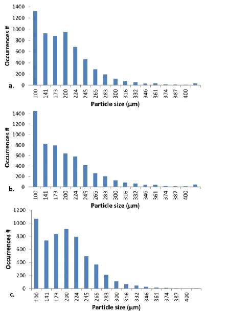
The XBSE images of the three composite samples are reported in Fig. 7. The darker parts of the sample (lower atomic number) corresponds to the epoxy areas while the brighter ones (higher atomic number) represent the ceramic particles. The MLA results for the three samples under test are summarized in Table IV. The ‘particle area %’ refers to the fraction of surface occupied by the mineral phase with respect to the total sample surface. The statistics of the particle areas are reported in Fig. 8.
TABLEIV RESULTS OF THE MLA ANALYSIS
Sample Total area (μm) Particle # Particle area %
BZT 204068452.41 6067 47%
CTNA 191443025.34 5605 44%
BNT 200722131.00 5679 47%
The results of the fitting of the dielectric data obtained from the SMM measurements with the 180 μm and 20 μm tip with those calculated via the numerical procedure described in the Experimental Methods section are reported in Table V.
In the 180 μm case, the three different samples are statistically described by volume filling 𝑉 with a monovariate Gaussian distribution as the permittivity data are concentrated around one value. The slightly asymmetric shape of the measured permittivity distribution is followed by the values generated numerically, which confirms that the Maxwell-Garnett approximation is applicable for this kind of tip-sample interaction. The results are plotted in Fig. 9.
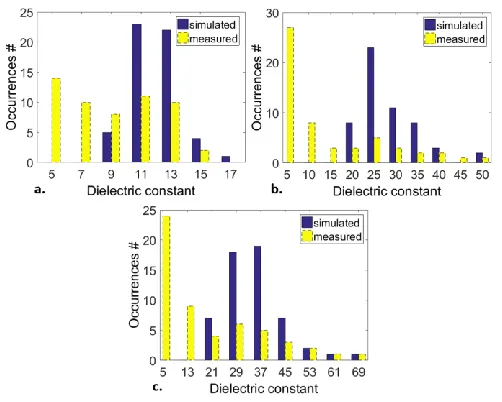
The results of the fitting for the 20 μm tip measurements are plotted in Fig. 10. In this case the permittivity distribution is concentrated around two peak values. It is clear that the statistical description of the interaction volume (in terms of filling fraction) is more complicated than in the former case, suggesting a bivariate distribution. It is interesting to see that, while the second peak in the distribution shifts towards higher values when the inclusion permittivity increases, the first peak remain fixed around 𝜀1𝑒𝑓𝑓~5 for all the samples. The higher peaks were fitted similarly to the 180 μm case (Table V).
TABLEV
GAUSSIAN DISTRIBUTION PARAMETERS
Tip μ
(BZT) σ (BZT)
μ (CTNA)
σ (CTNA)
μ (BNT)
σ (BNT) 180 m 0.55 0.12 0.52 0.12 0.55 0.12
20 m 0.65 0.06 0.8 0.06 0.8 0.06
[image:6.612.338.562.51.355.2]Parameters of the Gaussian distribution used for modelling the volume filling fraction.
Fig. 7. XBSE images of the samples: the darker areas corresponds to epoxy while the brighter to ceramic particles. a. is the BZT inclusions sample, b. is the CTNA inclusions sample and c. is the BNT one. The scale bars represent
2 mm. The average inclusion size is around 200 μm. Fig. 8. Histogram of the distribution of the particle areas from MLA analysis.
[image:6.612.49.297.258.338.2] [image:6.612.314.562.478.679.2]The fitting was performed with a total number of occurrences equal to the actual number of measurements. For this reason, in the latter case (20 μm) the fittings of the higher peaks are just qualitative. The fittings follow the distribution profile of the measured data although the numbers of values within each bin of the histograms do not match.
D. COMSOL© Model
A numerical model of the tip-sample interaction was developed using the ACDC module of COMSOL Multiphysics© (version 4.4). The volume of interaction beneath the tip is expected to be different for the two tips. In particular, the size and positions of the inclusions were chosen in order to simulate the average MLA results, reported in Table IV. An average size of 200 μm and rectangular section were considered. An image of the electric potential distribution (V) is shown in Fig. 11. For the simulations a reference voltage V0= 1 was applied to the tip while the surrounding shield representing the bottom plate of the resonator was grounded. The ratio between the length of the tip and the diameter of the resonator was chosen to match the real resonator, thus reproducing the combined effects of the electric field leaking through the aperture and the electric field produced by charge on the tip.
The values of the admittance Y were simulated at the reference port (the tip in this case). Accordingly, the difference in admittance values was compared between the same two positions for all the simulated samples. These results are given in Table VI under the “Min-max” column headings for each sample and are representative of the different tip-sample interactions for the three dielectric contrasts under analysis.
TABLEVI
COMPARISON BETWEEN THE SIMULATED ADMITTANCE VALUES
Tip
Min-Max (BZT)
Epoxy (BZT)
Min-Max (CTNA)
Epoxy (CTNA)
Min-Max (BNT)
Epoxy (BNT) 20 m 0.047 0.060 0.053 0.066 0.060 0.071 180 m 0.020 0.071 0.023 0.078 0.027 0.085 Comparison between the simulated admittance values for the tip interacting with the three different samples under analysis.
V. DISCUSSION
The simple COMSOL© model does not allow a direct derivation of the permittivity values but it is reasonable to assume that the admittances are related to the effective permittivity beneath the tip. The results of the simulations are in accordance with the statistical description of the tip-sample interaction of the previous section and show the physical meaning of such statistical description.
In particular, the differences between the 180 μm and 20 μm interacting tips are evident: in both cases the value obtained when the tip is placed between the inclusions (tip shift x = 160 μm hereby referred as ‘Min’) is different from the epoxy alone, even though there is epoxy directly under the tip. This is because the tip-sample interaction is volumetric and inclusions are partially present within the interaction volume. The reason for the absence of permittivity values close to 𝜀1𝑒𝑓𝑓= 3.2 (epoxy permittivity) in the measured data is clear. Even if the tip lands on an epoxy surface, the volume of interaction contains some fraction of the surrounding dielectric inclusions.
Additionally, these simulation results help in understanding why the 20 μm tip showed a large number of values in the bin 𝜀1𝑒𝑓𝑓~5, constant for the three samples under investigation (Fig. 10). The values in the columns labelled ‘Epoxy’ in Table VI are smaller for the 20 μm tip than for the 180 μm. The smaller tip has a smaller volume of interaction with the sample compared with the larger tip. When the smaller tip lands between inclusions, a greater volume fraction will be filled by epoxy and the volume fraction filled by the surrounding inclusions is less than for the larger tip. The effective Fig. 10. Fittings of the experimental data obtained with 20 μm tip
(yellow/dashed columns) with the statistical description based on Maxwell-Garnett effective medium approximation (blue/solid columns).
[image:7.612.321.562.47.226.2] [image:7.612.46.297.52.253.2] [image:7.612.308.576.278.340.2]permittivity is dominated by the epoxy and is therefore lower. Thus the first peak of permittivity around 5 can be attributed to the measurements done when the tip ‘landed’ on areas filled by epoxy, and is almost constant for the three dielectric contrasts considered in the experiment. The tails on the right hand side of the first peaks in Fig. 10 are due to intermediate situations when the tip ‘landed’ on epoxy but close to an inclusion. In order to highlight this effect, a further simulation with a 4 μm diameter tip was performed. The raw output of the 180 μm and 4 μm tip simulations is shown in Fig. 12 for comparison.
There is no sign of a split distribution of values of relative permittivity in the case of the 180 μm tip (Fig. 9), because the volume of interaction is large enough to always be intercepted by inclusions. The fitting parameters reported in Table V statistically represent the distribution of inclusions. The central value μ of the CTNA sample is slightly lower than the others and this is in accordance with the MLA analysis results. A further interesting observation arises from the second peaks of permittivity in the data from the 20 μm tip. The fitting parameters in this case are influenced by the dielectric contrast, defined as the difference between the relative permittivity of the ceramic and the epoxy. In the lowest
contrast sample, the BZT, 𝜇 = 0.65 whereas for the CTNA and BNT 𝜇 = 0.8.
This effect in the SMM data and COMSOL simulations is consistent with previous work on dielectric mixtures [31] where it was shown that a dielectric contrast of 10 is an empirical threshold between different models of the interaction between electromagnetic field and sample. There appears to be a need for a filling factor that takes into account the dielectric contrast as well as the geometrical distribution of inclusions within the volume of interaction beneath the tip of the SMM. Even though the samples are geometrically similar, as was shown by the MLA data, the fitting parameters for the second peak of the 20 μm data for the higher permittivity samples differed from that for the lowest permittivity sample. For the BZT data, where the dielectric contrast is below 10, 𝜇 = 0.65 is influenced by the geometry of the sample alone and it is the physical filling factor. In the CTNA and BNT data, where the dielectric contrast is above 10, the filling factor 𝜇 = 0.8 is higher, and contains contributions from both the actual filled volume and the dielectric contrast that further segregates the field into the inclusions.
VI. CONCLUSIONS
In this work a statistical approach is presented for the high-throughput dielectric characterization of multiphase materials samples. Scanning electron microscopy was used to characterize the topology and composition of multiphase dielectric samples. Experimental results match the effective medium description through the Maxwell-Garnett approximation for the portions of the sample under analysis for each measurement. In particular, by considering the fraction of volume of interaction filled by the inclusion (𝑉) as a statistical variable, measurements performed with 180 μm tip are described by a monovariate Gaussian distribution of 𝑉. Results of the measurements performed by 20 μm tip follows a bivariate distribution instead. In light of this statistical interpretation of the experimental results, the effect of the sample inhomogeneity with respect to the volume of interaction is explained.
The Inoue model of the tip-to-sample interaction was found more suitable for extraction of the permittivity than the image charge model of Gao and Xiang. The error bars for the calibration derived from the two models were similar, but the error bars for measurement of unknown permittivity are more straightforward to derive with the Inoue model. A complete uncertainty analysis considering the calibration set and practical factors such as sample positioning, tip-to-sample contact and the geometry of the resonator around the tip as tips are interchanged is required in future work.
[image:8.612.49.289.348.702.2]The SMM was designed for rapid interchange of probe tips. The lower bounds of dielectric loss that can be resolved by such an SMM are evaluated. The combination of a versatile instrument with statistical interpretation of high-throughput measurements allows exhaustive characterization of a relatively large sample in a short time. This new concept for SMM characterization can be potentially applied to Fig. 12. Admittance value profile obtained by COMSOL© ACDC model of
applications areas, such as production chains or material handling systems, where multiphase materials are employed and topology and composition information are partially known a priori.
ACKNOWLEDGMENTS
We would like to thank Mr Yangchun Li for preparatory work on the SMM during his MSc project, Mr Mark Wager for fabrication of the SMM base-plates, Prof C.C. Constantinou for photography and Dr Xiaobang Shang for writing the MATLAB routine used to extract the resonant frequency and quality factor.
REFERENCES
[1] C. Gao, B. Hu, I. Takeuchi, K. S. Chang, X. D. Xiang, and G. Wang, “Quantitative scanning evanescent microwave microscopy and its applications in characterization of functional materials libraries,” Meas. Sci. Tech., vol. 16, no. 1, p. 248, Dec 2004.
[2] Z. Wei, Y.-T. Cui, E. Y. Ma, S. Johnston, Y. Yang, R. Chen, M. Kelly, Z.-X. Shen, and X. Chen, “Quantitative theory for probe-sample interaction with inhomogeneous perturbation in near-field scanning microwave microscopy,” IEEE Trans. Micr. Theory Techn., vol. 64, no. 5, pp. 1402-1408, May 2016.
[3] T. Monti, P. Iezzi, M. Farina, and S. W. Kingman, “Full electromagnetic simulation of a scanning microwave microscope for quantitative estimation of material properties,” in 2015 1st URSI Atlantic Radio Science Conference (URSI AT-RASC), Gran Canaria, Spain, 2015, pp. 1-1.
[4] T. Monti, A. Di Donato, D. Mencarelli, G. Venanzoni, A.Morini, and M. Farina, “Near-Field Microwave Investigation of Electrical Properties of Graphene-ITO Electrodes for LED Applications,” J. Display Technol., vol. 9, pp. 504-510, Jun 2013.
[5] S. Safari, A. Castellazzi, and P. Wheeler, “Experimental and Analytical Performance Evaluation of SiC Power Devices in the Matrix Converter,” IEEE Trans. Pow. Electron., vol. 29, no. 5, pp. 2584-2596, May 2014. [6] P. M. Meaney, A. P. Gregory, N. R. Epstein, and K. D. Paulsen,
“Microwave open-ended coaxial dielectric probe: interpretation of the sensing volume re-visited,” BMC Medic. Phys., vol. 14, no. 3, 11 pp., Jun 2014.
[7] T. Monti, A. Tselev, O. Udoudo, I. N. Ivanov, C. Dodds, and S. W. Kingman, “High-resolution dielectric characterization of minerals: A step towards understanding the basic interactions between microwaves and rocks,” Int. J. Miner. Process., vol. 151, pp. 8-21, Jun 2016. [8] R. Meisels, M. Toifl, P. Hartlieb, F. Kuchar, and T. Antretter,
“Microwave propagation and absorption and its thermo-mechanical consequences in heterogeneous rocks,” Int. J. Miner. Process., vol. 135, pp. 40–51, Feb 2015.
[9] M. F. Córdoba-Erazo and T. M. Weller, “Noncontact electrical characterization of printed resistors using microwave microscopy,” IEEE Trans. Instr. Meas.., vol. 64, no. 2, pp. 509-515, Feb 2015. [10] S. M. Anlage, V. V. Talanov, and A. R. Schwartz, “Principles of
Near-Field Microwave Microscopy,” in Scanning Probe Microscopy, S. Kalinin, A. Gruverman, Springer, 2007, pp. 215-253.
[11] M. Tabib-Azar, D. Akinwande, G. Ponchak, and S. R. LeClair, “Novel physical sensors using evanescent microwave probes,” Rev. Sci. Instrum., vol. 70, no. 8, pp. 3381-3386, Aug 1999.
[12] J. D. Chisum and Z. Popovic, “Performance limitations and measurements analysis of a near-field microwave microscope for nondestructive and subsurface detection,” IEEE Trans. Microw. Theory Techn., vol. 60, no. 8, pp. 2605-2615, Aug 2012.
[13] M. Tabib-Azar and B. Sutapun, “Novel hydrogen sensors using evanescent microwave probes,” Rev. Sci. Instr., vol. 70, no. 9, pp. 3707– 3713, Sep 1999.
[14] C. Gao and X.-D. Xiang, “Quantitative microwave near-field microscopy of dielectric properties,” Rev. Sci. Instr., vol. 69, pp. 3846-3851, Nov 1998.
[15] T. Zhang and M. Tabib-Azar, “Calculation and accurate measurement of capacitance of electrically small axi-symmetric microstructures near a probe tip,” in 61stARFTG Conference Digest, Philadelphia (PA), pp. 147-156, Jun 2003.
[16] R. Inoue, Y. Odate, and E. Tanabe, “Data analysis of the extraction of dielectric properties from insulating substrates utilizing the evanescent perturbation method,” IEEE Trans. Micr. Theory Techn., vol. 54, no. 2, pp. 522-532, Feb 2006.
[17] R. J. Barlow, Statistics; John Wiley & Sons, New York, 1989, p. 100. [18] A. Shivola, Electromagnetic mixing formulas and applications; IEE,
London, 1999.
[19] W. R. Tinga, “Mixture laws and microwave-material interactions: Dielectric properties of heterogeneous materials,” Prog. Electrom. Res., vol. 6, pp. 1-34, 1992.
[20] T. Wei, X. D. Xiang, W. G. Wallace‐Freedman, and P. G. Schultz, “Scanning tip microwave near‐field microscope,” Appl. Phys. Lett., vol. 68, is. 24, pp. 3506-3508, Jun 1996.
[21] D. J. Barker, T. J. Jackson, P. M. Suherman, M. S. Gashinova, and M.J. Lancaster, “Uncertainties in the permittivity of thin films extracted from measurements with near field microwave microscopy calibrated by an image charge model,” Meas. Sc. Tech, vol. 15, no. 105601, 10 pp., Aug 2014.
[22] M. J. Lancaster, ch.4 in Passive Microwave Device Applications of High-Temperature Superconductors; Cambridge University Press, Cambridge, 1997.
[23] P. Petersan and S. M. Anlage, “Measurement of resonant frequency and quality factor of microwave resonators: Comparison of methods,” J. Appl. Phys., vol. 84, pp. 3392-3402, Sep 1998.
[24] M. Tabib-Azar, D. P. Su, A. Pohar, S. R. LeClair, and G. Ponchak, “0.4 μm spatial resolution with 1 GHz (λ= 30 cm) evanescent microwave probe,” Rev. Sci. Instr., vol. 70, is. 3, pp. 1725-1729, Mar 1999. [25] D.-Y. Sheu, “Micro-spherical probes machining by EDM,” J.
Micromech. Microeng., vol. 15, no. 1, pp. 185-189, Oct 2004.
[26] D. J. Barker, “Evaluation of microwave microscopy for dielectric characterisation,” Ph.D. dissertation, University of Birmingham, 2010. [27] S. Gevorgian, ch.4 in Ferroelectrics in Microwave Devices, Circuits and
Systems; Springer-Verlag, London, 2009, p. 118.
[28] R.M. Tennant, Science Data Book; Oliver&Boyd, Edinburgh, 1987. [29] G. Q. Jiang, W. H. Wong, E. Y. Raskovich, W. G. Clark, W. A. Hines,
and J. Sanny, “Measurement of the microwave dielectric constant for low‐loss samples with finite thickness using open‐ended coaxial‐line probes,” Rev. Sci. Instr., vol. 64, no. 6, pp. 1622-1626, Jun 1993. [30] P. J. Goodhew and F. J. Humphreys, ch. 5 in Electron Microscopy and
Analysis; Taylor and Francis, London, 1988.