Toward weak confinement regime in epitaxial nanostructures: Interdependence of spatial character
of quantum confinement and wave function extension in large and elongated quantum dots
A. Musiał,1,2,*P. Gold,3J. Andrzejewski,1A. L¨offler,3J. Misiewicz,1S. H¨ofling,3,4A. Forchel,3 M. Kamp,3G. S ˛ek,1and S. Reitzenstein2,3
1Institute of Physics, Wrocław University of Technology, Wybrze˙ze Wyspia´nskiego 27, 50-370 Wrocław, Poland 2Institute of Solid State Physics, Berlin University of Technology, Hardenbergstraße 36, D-10623 Berlin, Germany 3Technische Physik and Wilhelm-Conrad-R¨ontgen-Research Center for Complex Material Systems, University of W¨urzburg,
Am Hubland, D-97074 W¨urzburg, Germany
4School of Physics and Astronomy, University of St. Andrews, North Haugh, KY16 9SS St. Andrews, United Kingdom
(Received 15 April 2014; revised manuscript received 28 June 2014; published 31 July 2014) In this paper we present a comprehensive and detailed analysis of carrier/exciton wave function extension in large low-strain In0.3Ga0.7As quantum dots (QDs). They exhibit rather shallow confinement potential with
electron/hole localization energy below 30 meV and confinement strength substantially weakened in comparison to typical epitaxial quasi-zero-dimensional semiconductor nanostructures. The aim of this study is to investigate the influence of different factors on the wave function (probability density distribution) for carriers or excitons in this regime, i.e., object shape anisotropy as well as strain, piezoelectricity, and Coulomb interactions, and to identify the physical mechanisms determining the properties of optical emission. To probe the wave function symmetry, polarization-resolved photoluminescence has been performed, and the spatial extensions of the corresponding probability densities have been verified in magneto-optical measurements. The observed diamagnetic coefficients in the range of (15–31)μeV/T2 reflect large in-plane QD size. These studies also
enable us to investigate the importance of light hole states admixture to the valence band ground state in such nanostructures, which can be addressed via the degree of linear polarization of emission as well as the exciton
gXfactor. The linear-polarization-resolved measurements revealed an exceptionally low exciton fine structure splitting of 5μeV on average as well as a low emission polarization degree of−0.05, with the polarization perpendicular to the QD elongation direction dominating. The increased light hole contribution to the lowest energy hole level is reflected in the decreased excitongXfactor (in the range of 0–1) and is consistent with the results of the eight-bandk·pmodelling. Based on the temperature dependence of the diamagnetic coefficient, the problem of individual QD uniformity has additionally been discussed. To evaluate the impact of the confinment potential and the structure geometry on the optical properties of the QDs, a comparison between the investigated dots and InAs/InGaAlAs/InP quantum dashes exhibiting a much deeper confining potential is presented. DOI:10.1103/PhysRevB.90.045430 PACS number(s): 78.67.Hc,73.21.La
I. INTRODUCTION
Due to rapidly developing nanotechnology and the related fabrication techniques, a wide variety of nano-object shapes and sizes can be easily obtained with nanoscale precision in different material systems. This gives an opportunity to engineer and control their electronic structures and the resulting optical properties. In view of quantum effects, two critically distinct domains need to be distinguished, namely the strong and weak confinement regimes [1,2]. The criteria for domination of the confinement effects are (i) the quantization energy being much larger than the exciton binding energy, i.e., the energy scale characteristic for Coulomb interactions between the carriers confined in a quantum dot (QD), and (ii) the volume of the exciton (defined by the exciton Bohr radius) being larger than the physical volume of the nanostructure. The strong confinement regime is typical for epitaxial QDs due to their sizes in the range of few up to tens of nanometers. The quantized electron (hole) energy level separation for typical indium arsenide QDs is in the range of 50–200 meV (25–150 meV) and 40 meV (25 meV) for InAs/GaAs [3–7] and in the InAs/InP material
*Corresponding author: [email protected]
determined more and more by Coulomb interactions up to sizes where the three-dimensional energy quantization is preserved. Although it is relatively easy to predict the qualitative behavior of these nano-objects in the asymptotic cases (very weak and very strong confinement), it is much more difficult to make accurate predictions in the intermediate regime between weak and strong confinement without incorporating details of the actual physical system. In these cases, interpretation of experimental data is less straightforward.
The structures under study—In0.3Ga0.7As QDs—differ substantially from typical epitaxial QDs in terms of the confinement regime. Assuming linear interpolation between InAs (33 nm) and GaAs (12 nm) [11], the exciton Bohr radius for 30% indium InGaAs equals 18 nm, which results in the exciton volume being only 2.5 times larger than the physical volume of the nanostructure. Some optical signatures con-firming the weakened confining potential expected for these structures have already been reported [16,17]. Time-resolved measurements performed on both a QD ensemble, as well as on single QDs, confirmed the enhanced OS and revealed lifetimes of excitonic transitions as short as 350 ps [16,18], which enabled the first observation of strong coupling between a single exciton and a single photon in a micropillar cavity [15] and makes them useful for both fundamental studies and for applications, e.g., as an efficient source of single photons. A demonstration of the weakened confinement strength was the magnetic field-driven transition from strong to weak exciton-photon coupling in this system [16]. Experiments on exciton-biexciton cascade kinetics [17], in which the biexciton lifetime was counterintuitively found to be either comparable to or longer than the exciton one, allowed another signature of weakened confining potential to be identified [12].
In this paper we focus on a detailed analysis of the inter-dependence of the wave function extension and the confining potential in the case of large and elongated In0.3Ga0.7As/GaAs QDs exhibiting characteristics of confinement unique for epitaxial nanostructures. To better determine the confinement regime, eight-band k·p calculations have been performed and the characteristic energy scales of quantized single particle states and Coulomb interactions, included within the Hartree approximation, have been compared. The energy criterion confirms that the confining potential is weakened and can be classified as being in the intermediate regime with an exciton binding energy (of approximately 6 meV) comparable to the electron level separation (7 meV) and much larger than the interlevel spacing of the hole states (below 0.5 meV).
The paper is organized as follows. In Sec. II, the inves-tigated structures and the experimental setups are described. SectionIIIis devoted to polarization-resolved measurements followed by eight-bandk·pmodeling aimed at revealing the symmetry of the wave function and the factors influencing it. It also contains the comparison between polarization properties of the investigated dots and InAs/InGaAlAs/InP quantum dashes (QDashes), which we use to evaluate the impact of the confinement potential depth. In Sec.IV, a detailed study of magneto-optical properties (e.g., diamagnetic coefficient and exciton gX factor) probing the excitonic wave function
extension is presented. SectionVconcludes the paper.
II. SAMPLE AND EXPERIMENTAL SETUP
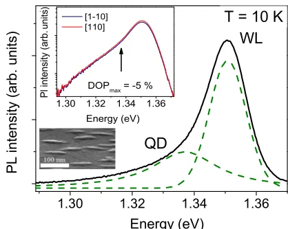
The investigated structures were grown by molecular beam epitaxy utilizing self-assembled formation within the Stranski-Krastanow growth mode. The indium content of 30% leads to low strain conditions due to relatively low (2%) lattice mismatch between the QD material and the GaAs substrate. These peculiar growth conditions result in the growth of large QDs with a surface density in the range of 6–9×109 cm−2(the latter facilitates single QD spectroscopy), which are elongated in one of the lateral directions coinciding with [1¯10] the crystallographic axis. A scanning electron microscopy (SEM) image of an uncapped sample, which was grown under similar conditions as the samples studied, is presented in the bottom inset of Fig. 1. The lateral QD dimensions before overgrowth are on the order of 50–80 nm and 20–30 nm, respectively, resulting in a lateral aspect ratio (LAR) of approximately two or more and height (the direction providing the strongest confinement) in the range of a few nanometers. The investigated structures were realized by submonolayer deposition of 30 alternating In0.12Ga0.88As/InAs sequences of 0.12 nm and 0.03 nm thicknesses, respectively. The deposited material is estimated to be 4.5 nm thick based on the growth conditions, of which 2.7 nm constitutes the wetting layer (WL) [19]. Further details of the growth procedure are given elsewhere [20]. Previous optical studies on such nanostructures have revealed that not only is the spatial confinement weaker than in standard QDs due to the increased nanostructure size [17], but that also the confining potential is very shallow (in the sense of the potential depth with respect to the barrier height). This is manifested by a low-temperature emission energy difference between the QD and WL emission bands as low as 25 meV [19]. It has important implications, especially for carrier dynamics [18,21], and allows for thermally activated energy/carrier transfer between the WL and the QD ensemble as well as the WL-mediated carrier redistribution [18].
units)
FIG. 1. (Color online) Low-temperature (10 K) ensemble photo-luminescence (PL) spectra (black solid line) decomposed into two Gaussian peaks corresponding to two emission bands of the wetting layer (WL) and of In0.3Ga0.7As/GaAs elongated QDs (green dashed
[image:2.608.329.538.512.679.2]Polarization-resolved photoluminescence (PL) measure-ments on the ensemble of nanostructures were realized on unpatterned samples using a standard far-field free-space experimental configuration with a 0.55 m focal length single-grating monochromator equipped with a liquid-nitrogen-cooled InGaAs multichannel linear detector, and an overall spectral resolution of about 100 μeV. The samples were mounted in a liquid helium continuous-flow cryostat and cooled down to 5 K. The continuous wave excitation was provided by a semiconductor laser in a nonresonant manner with a 660 nm wavelength beam focused on the sample surface to a spot of approximately 100μm diameter by employing long focal length optics.
To perform the measurements on a single QD, the spatial resolution was increased by using samples with submicrom-eter mesas patterned lithographically by electron-beam and wet chemical etching. For magneto-optical experiments and investigations on the fine structure splitting (FSS), a high resolution micro-PL setup equipped with a frequency doubled Nd:YAG solid state laser (532 nm), microscope objective (numerical aperture 0.4) and 0.75 m focal length single-grating monochromator, and a Si charge-coupled device (CCD) detec-tor providing a spectral resolution of approximately 30μeV was used. The sample was mounted inside a magneto-optical cryostat enabling the application of constant homogeneous magnetic fields up to 5 T in the Faraday configuration and variation of the temperature in a wide range between 5 K and room temperature.
For polarization-resolved PL, rotatable quarter- or half-wave plates together with a fixed linear polarizer were used in the detection path to exclude the polarization characteristics of the spectrometer.
III. WAVE FUNCTION SYMMETRY A. Degree of linear polarization of the surface emission An important figure of merit in the following experiments is the degree of linear polarization (DOP) of surface emission obtained at the maximum of the QD ensemble emission band. It describes the dominance of one of the linear polarization components over another:
DOP= II I −I⊥
II I +I⊥
, (1)
with II I and I⊥ being the intensity of surface emission
polarized in the direction longitudinal and transverse to the structure elongation. Lowering the in-plane confinement potential symmetry results in a ground hole state of a mixed character (of light and heavy hole—lh and hh, respectively), which leads to a lifting of the ground state degeneracy and two unequal linearly polarized components [22]. The emission intensity ratio of the two states is determined by the degree of the valence band mixing. The cause of the valence band mixing can be complex, i.e., anisotropic strain distribution [22,23], nanostructure shape anisotropy (proven for strain-free QDs grown by droplet epitaxy method [24]), and increased nanostructure height resulting in decreased lh-hh energy separation [25,26]. In the first approximation two linearly polarized components are orthogonal and in the direction determined by the structure geometry. When more
subtle effects on the single dot level are taken into account (i.e., local strain distribution in the vicinity of an individual QD), both the direction and the angle between different components can vary significantly from dot to dot [27–29]. Measurements presented in this subsection have been performed on the QD ensemble to average these effects. The preferential directions of linear components have been carefully checked and appear to coincide with the crystallographic axes parallel and perpendicular to the structure elongation direction [1¯10].
In Fig. 1, a low-temperature (10 K) PL spectrum is presented. Two emission bands can be resolved: the PL band related to the QD ensemble with an inhomogeneous broadening of approximately 30 meV, reflecting the size and composition distribution, and the WL-related PL. The emission bands overlap significantly due to shallow confining potential of the QDs and the low-energy tail of the WL density of states related to the thickness/composition fluctuations of the WL quantum well. Polarization-resolved measurements were performed at 5 K and reveal DOP values at the maximum of the QD ensemble emission on the order of
combined with the temperature dependence of the diamagnetic coefficient discussed in Sec.III C, lead to the conclusion that in this case additional localization within the nanostructure is rather unlikely and should not dominate the effective optical response of the QD ensemble and, hence, cannot explain the low experimental DOP values.
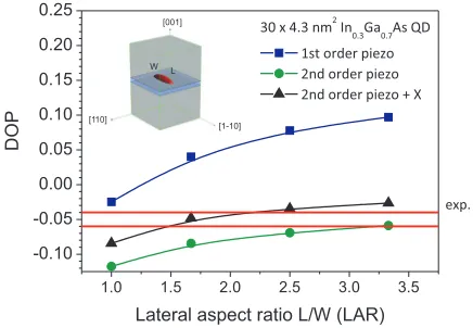
To understand the physical effects behind the observed low and negative value of DOP, numerical simulations have been performed. To model the polarization properties of QDs, an accurate description of the band mixing is required; therefore, the full eight-band k·p Hamiltonian was used, including realistic strain distribution and piezoelectric effects (up to the second order). A more detailed analysis of the utilized theoretical approach can be found elsewhere [36,37]. To study the influence of the excitonic effects, the Coulomb interactions between carriers confined in the QD have been included within the Hartree model. This leads to the modification in the wave function and, as a result, the OS of respective transitions and correction in the emission energy by the exciton binding energy. To obtain the dependence of DOP on the LAR, the OS of the optical transitions for different polarization components has been calculated. The QD lengthLwas varied, while the base widthW and heightH were left unchanged and equal to 30 nm and 4.3 nm, respectively, in agreement with the existing structural data [20]. A lens-shaped QD geometry and a 2.7-nm-thick WL have been assumed based on available data for the InGaAs/GaAs material system [38]. The scheme of the system geometry (QD: red; WL: blue) used in the calculations together with numerical box (gray) is depicted in the inset of Fig.2.
The results of the calculated DOP dependence on the QD lateral geometry including different effects are shown in Fig.2. In the first attempt, the excitonic effects have not been included in these considerations. This is justified because the valence
1.0 1.5 2.0 2.5 3.0 3.5
-0.10 -0.05 0.00 0.05 0.10 0.15 0.20 0.25
30 x 4.3 nm2In0.3Ga0.7As QD 1st order piezo 2nd order piezo 2nd order piezo + X
DOP
Lateral aspect ratio L/W (LAR)
exp.
[001]
[1-10] [110]
L W
FIG. 2. (Color online) Full eight-bandk·pcalculation results of the DOP dependence on LAR for 30×4.3 nm2 In
0.3Ga0.7As QDs
including only first-order piezoelectric effect (blue squares), both first- and second-order piezoelectric effect (green dots) in the single particle picture, Coulomb interactions (black triangles) with solid lines being only guides to the eye, and the range of experimentally observed DOP values marked by red horizontal lines. Inset: Schematic representation of an In0.3Ga0.7As QD structure geometry used in
eight-bandk·pcalculations showing quantum box size (gray), WL (blue), and QD (red).
band mixing primarily determines the polarization properties of emission. The admixture of the lh states into the hole ground state is in the range of 1.9–2.7% (depending on the LAR); as a result, DOP is nonzero. If the first-order piezoelectric effect exclusively is included, a negative value of DOP can be reproduced only for isotropic QDs, as can be seen in Fig.2 (blue squares), for which DOP equals to −0.025 (absolute value smaller than observed experimentally). With increasing length of the QD, the DOP changes its sign and increases smoothly up to 0.1 for QD lengths as large as 100 nm (LAR above 3), i.e., certainly above the typical elongation of the investigated structures. In the case of preserved QD symmetry, the piezoelectric field favors the [110] direction leading to negative DOP values, but as the QD elongation is increased, the influence of the confining potential anisotropy starts to dominate. Clearly the linear piezoelectric effect cannot explain the outcome of polarization-resolved measurements. Including second-order piezoelectric effects appears to be sufficient to explain the negative DOP in a wider range of geometries (green dots in Fig.2) [39–41]. Even though there is no quantitative correspondence to the experimental data in the realistic LAR range, we could conclude that the nonlinear piezoelectric field can be identified as the physical mechanism enforcing the negative sign of DOP. As the QD gets elongated, the absolute value of DOP decreases (the emission becomes less polarized). This is due to the increasing extension of the wave function in the elongation direction. Thus, the observed DOP is a result of the interplay between these two major effects, where the elongation cannot compensate for the inherent piezoelectric field anisotropy.
Adding Coulomb interactions to this picture does not change the results qualitatively. It shifts the whole DOP dependence upwards by around 0.04 as it is an additional factor compensating for the piezoeletricity-induced wave function anisotropy (black triangles in Fig. 2). This is explained by Coulombic attraction between electrons and holes and the overall tendency for the probability densities to symmetrize. This correction appears to be sufficient to account for the experimental observations and enables us to deduce a LAR in the range of 1.5–2, in agreement with expected in-plane QD geometry.
[image:4.608.64.282.486.637.2](a) 30 x 30 x 4.3 nm3 QD
30 x 75 x 4.3 nm3 QD electron
electron
hole
hole
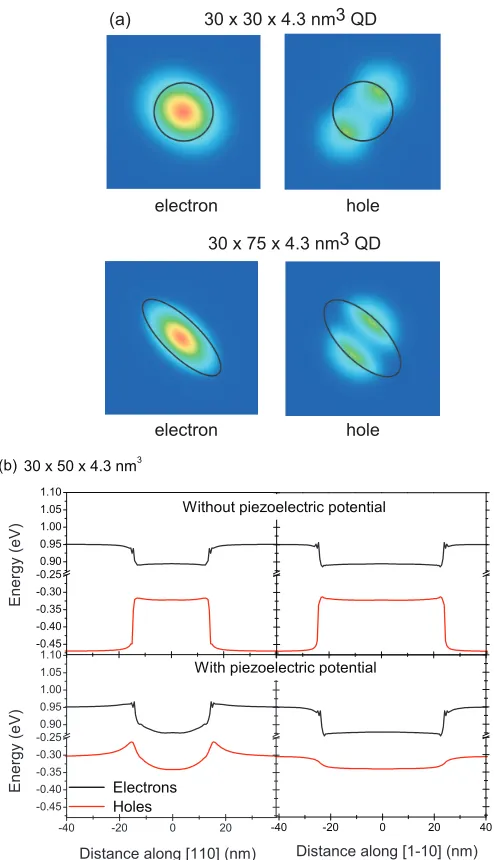
FIG. 3. (Color online) (a) Calculated electron (left) and hole (right) density function probabilities in the vertical (growth) direction for In0.3Ga0.7As/GaAs QDs on the WL for a symmetric (top) and
asymmetric (bottom) QD in the single particle picture. The black contour shows QD shape/size assumed in the calculations. (b) Calculated confining potential cross sections along the[110] (left) and [1¯10] directions without (top panel) and with (bottom panel) piezoelectric potential up to the second order for 30×50×4.3 nm3
QD geometry.
the impact of the confining potential details on the symmetry of the electron and hole wave functions. Due to the combined effect of the barrier potential height (band gap discontinuity), strain-induced band offset and piezoelectric potential, rather shallow confinement is obtained. The most important differ-ence regarding the piezoelectric potential is that its inclusion makes the confinement potential deeper for electrons and shallower for the holes. This can be clearly seen in Fig.3(b) where the cross sections of confining potential along the short (left) and long (right) QD axes without (top panel) and with (bottom panel) the piezoelectric potential are compared. As a
consequence, the symmetry of the electron wave function is determined by the QD physical shape. The situation differs for the hole states with anisotropic effective mass, which are much more susceptible to the piezoelectric field, which can overcome the spatial confinement and defines the main optical axis.
To emphasize the influence of confinement potential depth on the polarization properties of emission, we have compared the investigated structures with other elongated nanostructures—InAs/InGaAlAs/InP QDashes (LAR exceed-ing 5) [42–45]. Such InP-based structures exhibit much deeper confinement potential for both types of carriers, i.e., by definition expected to be much less sensitive to the peculiarities of the confining potential shape. But on the other hand, the QDashes are similar to the investigated In0.3Ga0.7As/GaAs QDs with respect to the lack of in-plane rotational symmetry and the resulting lh contribution to the excitonic states. Much higher DOP—in the range of 0.15 up to 0.3—was observed experimentally [34,46]. This can be traced back to a larger lh contribution to the valence band ground state, in the range of 3.2–5.1% for QDash structures. In the case of the investigated In0.3Ga0.7As QDs, it equals only 1.9–2.7%, depending on the LAR. Numerical calculations similar to those presented in this paper predict DOP reaching up to 0.3 for strongly anisotropic objects, corresponding well with the experimental data [37]. Negative DOP values have not been observed experimentally or predicted theoretically. This striking difference can be attributed to the wave function symmetry, which in this case corresponds better to the shape of the nanostructure due to stronger confinement of the carriers inside a relatively deep potential well. The activation energy with respect to the WL for a typical QDash is about 118 meV (54 meV) for electrons (holes) [47], in comparison to 29 meV (19.6 meV) calculated for the investigated In0.3Ga0.7As QDs. The presented considerations prove that in the case of shallow confining potential, the wave function sensitivity to the details of QD shape is reduced and can be further diminished by the weakened confinement. This brings one to the conclusion that for quasi-zero-dimensional systems where the carriers are not strongly confined, the interpretation of polarization-resolved measurements as well as predictions on the polarization properties of emission are not straightforward. This is very important in view of applications, especially in optoelectronics or nanophotonics, because of the demand for some devices to be entirely polarization insensitive (e.g., optical amplifiers) and others having preferable polarization direction (e.g., lasers or single photon sources for applications in the field of quan-tum cryptography). There are solutions based on additional external controlling systems changing the polarization state or filtering out the unwanted components [48], but they are always accompanied by increased losses (which require being balanced by increased source efficiency—commonly already pushed to the limits), more complicated fabrication processes, or significantly less compact device designs. It would be prefer-able if the polarization of light suitprefer-able for specific applications could be selected based on the design of the active region alone.
B. Exciton FSS
[image:5.608.50.297.69.499.2]PL
intensity (arb. units)
PL
intensity (arb. units)
Sine function fit
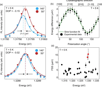
FIG. 4. (Color online) μPL spectra of two single QDs with DOPs of (a)−0.15 and (c)−0.02, respectively, measured for two orthogonal polarization directions. (b) Corresponding polarization angle emission energy dependence of (a), from which the FSS has been extracted. (d) FSS dependence on exciton emission energy obtained experimentally with error bars estimated based on single emission line fitting procedure uncertainty.
ground state is fourfold degenerate due to two possible
z components of the electron spins (±1/2) and the hole angular momenta (±3/2). Two of these exciton states carry angular momentum of two and are dipole forbidden (dark excitons), whereas the remaining two are circularly polarized (angular momentum equals±1) and optically active (bright excitons). The electron-hole exchange interaction lifts this degeneracy completely and mixes states with well-defined angular momenta, which results in linearly polarized exciton eigenstates [49]. The energy splitting between the two bright excitons, so-called FSS resulting from the anisotropic part of this interaction [50], is caused by lowering the symmetry of the confining potential. When considered on the atomistic level, it can be related to the crystal lattice symmetry and its disturbance due to atomic strain relaxation at the interfaces [7,51]. The resulting splitting is being referred to as intrinsic FSS and is generally on the order of a single micro-electron-volt. Other mechanisms leading to lowering of the confining potential symmetry are shape asymmetry and strain-induced piezoelectric fields [5]. The FSS can be determined experimentally in polarization-resolved PL because the nondegenerate optically active excitonic states have orthogonal linear polarizations. This can be seen in
[image:6.608.101.506.73.418.2]be seen in Fig.4(d), where the FSS is plotted as a function of the QD emission energy. The result is again counterintuitive when taking only the pronounced in-plane asymmetry of the In0.3Ga0.7As QDs into account. We would like to point out that the average FSS is significantly lower than values observed for standard InGaAs QDs in a GaAs matrix [49,52– 54]. It is even close to the values observed for strain-free GaAs/AlGaAs QDs [55] or In(Ga)As QDs grown on (111)-oriented GaAs [56–59], which makes the In0.3Ga0.7As appealing for the generation of polarization entangled photon pairs using the biexciton-exciton cascade [59,60]. The reason for the confinement potential asymmetry not to be manifested in increased FSS may be the same as for the low DOP of emission—the shallow confining potential causing lower sensitivity of the wave function symmetry to the details of the QD shape due to its extension being much smaller than the potential size. This result is significant, not only in view of fundamental research, pointing out that very small FSS does not necessarily require highly symmetric QDs, but also in consideration of the applications, especially those relying on photon indistinguishability and entanglement [61–64].
Additionally, no correlation between the magnitude of the FSS and the exciton emission energy has been observed, as presented in Fig.4(d)[65]. Normally the spectral distribution of the FSS is used to examine its dependence on the QD size [66–68], but in the case of low In content InGaAs/GaAs QDs, it is not straightforward as the emission energy is driven by more than one factor and the influence of each of them is not easy to extract due to the self-organized character of QD formation resulting in per-dot differences in shape, size, and composition. The study of InGaAs QD samples differing strongly in composition has revealed a clear correlation between the QD size and the In content—the higher the In content, the smaller the size of the nanostructure due to increased lattice mismatch and the resulting strain. This trend can also be observed on a smaller scale, i.e., within one QD sample with a given nominal In content. We discuss this in more detail in Sec.IV A. Even with this additional information, predictions of the FSS dependence on the exciton emission energy cannot be easily made due to the complex influence of In on the emission energy. The In content changes the bandgap energy as well as the lattice constant of the InGaAs alloy. The former influences the emission energy directly, and the latter affects the lattice mismatch with the GaAs substrate and varies the strain, which further determines the QD size and, as a result, the part of the emission energy related to the electronic structure of the QD. These effects are competing as they induce opposing changes in the emission energy. The secondary effect is the tendency of In to segregate, which is also composition dependent.
IV. WAVE FUNCTION EXTENSION A. Diamagnetic coefficient
To examine in detail the wave function extension, we performed single QD magneto-optical studies up to 5 T. From the energy position of individual QD emission lines we determined the diamagnetic coefficient assuming a quadratic energy shift as a function of magnetic field. This is justified
in our experimental conditions (weak magnetic fields) due to much smaller cyclotron energy when compared to the exciton binding energy of the investigated structures [4,9,69,70]. In this case, the diamagnetic coefficientκ can be expressed as follows [71]:
κ = e
2
8
ρ2
e
me
+
ρ2
h
mh
,
where ρ2 is the average quadratic extension of the wave function, me stands for the in-plane effective mass of an
electron, and mh for the average hole effective mass. The
exciton wave function has been probed experimentally, and by substituting the carrier effective mass with the exciton reduced mass the mean lateral extension of the exciton wave function 2
ρX2has been obtained. We would like to point out that the diamagnetic coefficient probes only the wave function average extension (radius) in the smallest direction perpendicular to the orientation of the applied magnetic field but does not give any information about its symmetry, which should be deduced independently.
Diamagnetic coefficients determined experimentally for In0.3Ga0.7As elongated QDs in the Faraday configuration are in the range of 15–31 μeV/T2 [Fig. 5(c)], which are significantly larger than values reported for other In(Ga)As QDs [16,72–74]—typically less than several micro-electron-volts per square of the magnetic field. This result is not surprising taking into account the low In content leading to an increased exciton Bohr radius in these nanostructures [15–17]. A more detailed investigation has revealed an increasing diamagnetic coefficient as a function of the emission energy, as presented in Fig.5(c). The observed tendency cannot be simply related to the size of the QDs because in that case the opposite trend would be expected—smaller QDs with higher emission energy should exhibit lower diamagnetic coefficients due to stronger wave function confinement. Thus, changes in emission energy seem to be of more complicated origin being a result of the interplay between the QD size and the indium content. The increase of the diamagnetic coefficient for larger emission energy suggests that the emission in this spectral range originates preferentially from larger QDs within the ensemble of emitters. This can be explained by a lower In content of these QDs, which is in agreement with the trend observed for higher In content variation: indium-rich QDs with 60% In are smaller than 30% In nanostructures mainly due to lowering the lattice mismatch with respect to the GaAs matrix [20], but they emit at longer wavelengths as a result of band gap shrinkage due to the larger In mole fraction. As a result, the emission energy is higher for larger QDs, which is in qualitative agreement with the trend observed in magneto-optical experiments. The dependence of the diamagnetic coefficient as a function of the emission energy can be interpreted as simultaneous size and In content variation within the QD ensemble.
FIG. 5. (Color online) (a) Magnetic field dependence of diamagnetic shift for a single elongated In0.3Ga0.7As/GaAs QD for different
temperatures in the range from 7 to 35 K with linear fit (straight line) to experimental data (dots). (b) Temperature dependence of the diamagnetic coefficient for three exemplary QDs exhibiting qualitatively different behavior. (c) Experimentally obtained dependence of diamagnetic coefficient on emission energy.
experimental data. Further study revealed distinctive behavior of the diamagnetic coefficient as a function of temperature for different QDs. In Fig.5(b), examples of three qualitatively different behaviors are shown, i.e., the temperature dependence of the diamagnetic coefficient is plotted for three QDs. These different types of behavior can be classified based on the low-temperature value of the diamagnetic coefficient. For QDs showing the highest diamagnetic coefficients, a sharp increase with temperature has been observed, e.g., from 30 up to 41μeV/T2at 35 K[QD1 in Fig.5(b)]. For the intermediate case of 24μeV/T2, the increase is much more subtle, about 10% in the same temperature range (QD2). In the case of the smallest diamagnetic coefficient—21 μeV/T2—no clear temperature dependence can be observed (QD3). All these observations can be understood as follows: a large value of the diamagnetic coefficient corresponds to a large wave function extension resulting from weaker confinement for carriers than in the case of smaller QDs. An abrupt change in the diamagnetic coefficient with temperature is a manifestation of spreading the probability density over the entire QD structure from being confined at a local minima of potential originating from, e.g., QD height or In content fluctuations on the scale of individual QDs. The latter is in agreement with premises from PL-quenching measurements on individual QDs where small activation energy has been observed in some cases [35]. On the other hand, when the low temperature value of the diamagnetic coefficient is relatively small and it does not change with temperature, we are dealing with a QD exhibiting stronger quantum confinement (smaller size lowering the probability of additional trapping centers appearing), and the wave function is extended over the entire QD volume already at 5 K, which is why the temperature has no significant impact on the diamagnetic coefficient.
B. ExcitonicgXfactor
Magneto-optical measurements on single QDs have also enabled us to extract the excitonic Land´egXfactor from the
Zeeman splitting dependence on the magnetic field. Excitonic
gXfactors obtained for In0.3Ga0.7As QDs under the assumption of a linear dependence of the Zeeman splitting on the magnetic field are in the range of 0–1 (Fig.6), significantly lower than for In-rich smaller QDs for which the values of approximately 3 have been reported [72]. Also, the interdependence between the diamagnetic coefficient andgX factor values character is
reversed—largergX factors are characteristic for structures
exhibiting low diamagnetic coefficients (Fig. 6). This can be explained by an increased lh component in the valence band states of elongated QDs (weaker confinement of holes enhances further the states mixing in the valence band). The excitonic Land´egX factor is composed of hole and electron
contributions. It is well established that the hole gh factor
is much more sensitive to the details of QD size, shape, and composition than the electron ge factor [75–77]. For
the in-plane symmetric flat nanostructures, the hh component with higherghhfactor dominates (especially in self-assembled structures under the compressive strain), but the admixture of the lh states increases with increasing QD elongation resulting in lowering the holeghfactor and, as a consequence, also the
[image:8.608.58.557.72.241.2]excitonicgXfactor.
[image:8.608.314.555.560.723.2]V. CONCLUSIONS
High resolution optical and magneto-optical spectroscopy combined with numerical calculations based on eight-bandk·p theory has been used to examine the wave function extension and its symmetry in large In0.3Ga0.7As/GaAs QDs. In spite of the significant shape anisotropy of these nanostructures, we detected the smallest values of the ground state exciton FSS when compared to any epitaxial InGaAs/GaAs QDs on (001)-oriented GaAs substrate, which is highly attractive for the generation of polarization entangled photon pairs. Despite pronounced shape asymmetry, the DOP of the In0.3Ga0.7As QDs has a surprisingly low value, in the range of a single percentage, with the main optical axis perpendicular to the QD elongation. This has been attributed to the anisotropy of the nonlinear piezoelectric field, which dominates over the effect of spatial confinement symmetry. In addition, shallow confining potential makes the wave function less sensitive to the QD shape changes, especially for the hole states. Polarization-resolved measurements show that the high in-plane anisotropy is not sufficient for DOP to be large. In the case of shallow and weakened confining potential, DOP cannot be used as a probe of lateral shape or confining potential
symmetry as it rather reflects the symmetry of the wave function, which is driven by more factors than the structure shape itself. In comparison to more common higher In content InGaAs QDs, the obtained diamagnetic coefficient is larger, and thegXfactor is smaller. The former confirms larger wave
function extension, whereas the latter is related to increased valence band mixing (decreasedghfactor) resulting from the
QD shape anisotropy. The obtained exciton wave function extensions prove a weakened confining potential implying non-negligible influence of the Coulomb interactions in such dots.
ACKNOWLEDGMENTS
The work has financially been supported by the Grant No. 2011/02/A/ST3/00152 of the National Science Center of Poland. The experiments have partially been performed within the laboratory infrastructure at Wroclaw University of Technology financed by the Polish Ministry of Science and Higher Education Grant No. 6167/IA/119/2012. A.F. and J.M. gratefully acknowledge the Foundation for Polish Science (FNP) and Deutsche Forschungsgemeinschaft (DFG) for financial support within the COPERNICUS Award.
[1]Semiconductor Quantum Dots, edited by L. Banyai and S. W. Koch (World Scientific Publishing, New York, 1993).
[2] R. C. Iotti and L. C. Andreani, Phys. Rev. B 56, 3922 (1997).
[3] C. Pryor,Phys. Rev. B57,7190(1998).
[4] Ph. Lelong, O. Heller, and G. Bastard,Solid State Electron.42, 1251(1998).
[5] M. Grundmann, O. Stier, and D. Bimberg, Phys. Rev. B52, 11969(1995).
[6] M. Grundmann, N. N. Ledentsov, O. Stier, D. Bimberg, V. M. Ustinov, P. S. Kop´ev, and Zh. I. Alferov,Appl. Phys. Lett.68, 979(1996).
[7] G. Bester and A. Zunger,Phys. Rev. B71,045318(2005). [8] R. J. Warburton, B. T. Miller, C. S. D¨urr, C. B¨odefeld, K. Karrai,
J. P. Kotthaus, G. Medeiros-Ribeiro, P. M. Petroff, and S. Huant, Phys. Rev. B58,16221(1998).
[9] G. A. Narvaez, G. Bester, and A. Zunger, Phys. Rev. B 72, 245318(2005).
[10] M. Syperek, Ł. Dusanowski, J. Andrzejewski, W. Rudno-Rudzi´nski, G. S ˛ek, J. Misiewicz, and F. Lelarge,Appl. Phys. Lett.103,083104(2013).
[11] Handbook Series on Semiconductor Parameters, edited by M. Levinshtein, S. Rumyantsev, and M. Shur (World Scientific, New York, 1996).
[12] M. Wimmer, S. V. Nair, and J. Shumway,Phys. Rev. B 73, 165305(2006).
[13] T. Takagahara,Phys. Rev. B36,9293(1987). [14] E. Hanamura,Phys. Rev. B37,1273(1988).
[15] J. P. Reithmaier, G. Sek, A. L¨offler, C. Hofmann, S. Kuhn, S. Reitzenstein, L. V. Keldysh, V. D. Kulakovskii, T. L. Reinecke, and A. Forchel,Nature432,197(2004).
[16] S. Reitzenstein, S. M¨unch, P. Franeck, A. Rahimi-Iman, A. L¨offler, S. H¨ofling, L. Worschech, and A. Forchel,Phys. Rev. Lett.103,127401(2009).
[17] G. S ˛ek, A. Musiał, P. Podemski, M. Syperek, J. Misiewicz, A. L¨offler, S. H¨ofling, L. Worschech, and A. Forchel,J. Appl. Phys.107,096106(2010).
[18] M. Syperek, A. Musiał, G. S ˛ek, P. Podemski, J. Misiewicz, A. L¨offler, S. H¨ofling, L. Worschech, and A. Forchel,AIP Conf. Proc.1399,563(2011).
[19] P. Poloczek, G. S ˛ek, J. Misiewicz, A. L¨offler, J. P. Reithmaier, and A. Forchel,J. Appl. Phys.100,013503(2006).
[20] A. L¨offler, J. P. Reithmaier, A. Forchel, A. Sauerwald, D. Peskes, T. K¨ummell, and G. Bacher, J. Crystal Growth 286, 6 (2006).
[21] M. Syperek, M. Baranowski, G. S ˛ek, J. Misiewicz, A. L¨offler, S. H¨ofling, S. Reitzenstein, M. Kamp, and A. Forchel, Phys. Rev. B87,125305(2013).
[22] A. V. Koudinov, I. A. Akimov, Yu. G. Kusrayev, and F. Henneberger,Phys. Rev. B70,241305(R) (2004).
[23] Y. L´eger, L. Besombes, L. Maingault, and H. Mariette,Phys. Rev. B76,045331(2007).
[24] T. Belhadj, T. Amand, A. Kunold, C.-M. Simon, T. Kuroda, M. Abbarchi, T. Mano, K. Sakoda, S. Kunz, X. Marie, and B. Urbaszek,Appl. Phys. Lett.97,051111(2010).
[25] Y. Ikeuchi, T. Inoue, M. Asada, Y. Harada, T. Kita, E. Taguchi, and H. Yasuda,Appl. Phys. Exp.4,062001(2011).
[26] D. Roy-Guay, P. J. Poole, and S. Raymond,Semicond. Sci. Tech. 25,045001(2010).
[27] S. Ohno, S. Adachi, R. Kaji, S. Muto, and H. Sasakura,Appl. Phys. Lett.98,161912(2011).
[28] C. Tonin, R. Hostein, V. Voliotis, R. Grousson, A. Lemaitre, and A. Martinez,Phys. Rev. B85,155303(2012).
[29] P. Kaczmarkiewicz, A. Musiał, G. S ˛ek, P. Podemski, P. Machnikowski, and J. Misiewicz, Acta Phys. Pol. A 119, 633 (2011).
[31] T. Mano, R. N¨otzel, G. J. Hamhuis, T. J. Eijkemans, and J. H. Wolter,Appl. Phys. Lett.81,1705(2002).
[32] A. D. G¨uc¸l¨u, C. J. Umrigar, Hong Jiang, and Harold U. Baranger, Phys. Rev. B80,201302(R) (2009).
[33] T. Guillet, R. Grousson, V. Voliotis, X. L. Wang, and M. Ogura, Phys. Rev. B68,045319(2003).
[34] A. Musiał, P. Kaczmarkiewicz, G. S ˛ek, P. Podemski, P. Machnikowski, J. Misiewicz, S. Hein, S. H¨ofling, and A. Forchel,Phys. Rev. B85,035314(2012).
[35] A. Musiał, G. S ˛ek, P. Podemski, J. Misiewicz, A. L¨offler, S. H¨ofling, S. Reitzenstein, J. P. Reithmaier, and A. Forchel, Acta Phys. Pol. A120, 883 (2011).
[36] J. Andrzejewski, G. Sek, E. O’Reilly, A. Fiore, and J. Misiewicz, J. Appl. Phys.107,073509(2010).
[37] J. Andrzejewski,J. Comput. Phys.249,22(2013).
[38] G. S ˛ek, P. Poloczek, K. Ryczko, J. Misiewicz, A. L¨offler, J. P. Reithmaier, and A. Forchel,J. Appl. Phys.100,103529(2006). [39] G. Bester, A. Zunger, X. Wu, and D. Vanderbilt,Phys. Rev. B
74,081305(R) (2006).
[40] A. Beya-Wakata, P.-Y. Prodhomme, and G. Bester,Phys. Rev. B84,195207(2011).
[41] A. Schliwa, M. Winkelnkemper, and D. Bimberg,Phys. Rev. B 76,205324(2007).
[42] J. P. Reithmaier, G. Eisenstein, and A. Forchel,Proc. IEEE95, 1779(2007).
[43] W. Rudno-Rudzi´nski, G. S ˛ek, K. Ryczko, R. Kudrawiec, J. Misiewicz, A. Somers, R. Schwertberger, J. P. Reithmaier, and A. Forchel,Appl. Phys. Lett.86,101904(2005).
[44] W. Rudno-Rudzi´nski, R. Kudrawiec, P. Podemski, G. S ˛ek, J. Misiewicz, A. Somers, R. Schwertberger, J. P. Reithmaier, and A. Forchel,Appl. Phys. Lett.89,031908(2006).
[45] G. S ˛ek, P. Podemski, A. Musiał, J. Misiewicz, S. Hein, S. H¨ofling, and A. Forchel,J. Appl. Phys.105,086104(2009). [46] A. Musiał, P. Podemski, G. S ˛ek, P. Kaczmarkiewicz,
J. Andrzejewski, P. Machnikowski, J. Misiewicz, S. Hein, A. Somers, S. H¨ofling, J. P. Reithmaier, and A. Forchel, Semicond. Sci. Tech.27,105022(2012).
[47] A. Musiał, Ph.D. dissertation, Institute of Physics, Wroclaw University of Technology, Wroclaw, Poland, 2013.
[48] T. Heindel, Ch. A. Kessler, M. Rau, Ch. Schneider, M. F¨urst, F. Hargart, W.-M. Schulz, M. Eichfelder, R. Roßbach, S. Nauerth, M. Lermer, H. Weier, M. Jetter, M. Kamp, S. Reitzenstein, S. H¨ofling, P. Michler, H. Weinfurter, and A. Forchel,New J. Phys.14,083001(2012).
[49] M. Bayer, G. Ortner, O. Stern, A. Kuther, A. A. Gorbunov, A. Forchel, P. Hawrylak, S. Fafard, K. Hinzer, T. L. Reinecke, S. N. Walck, J. P. Reithmaier, F. Klopf, and F. Sch¨afer,Phys. Rev. B65,195315(2002).
[50] E. Kadantsev and P. Hawrylak,Phys. Rev. B81,045311(2010). [51] G. Bester, S. Nair, and A. Zunger,Phys. Rev. B67,161306(R)
(2003).
[52] A. H¨ogele, S. Seidl, M. Kroner, K. Karrai, R. J. Warburton, B. D. Gerardot, and P. M. Petroff,Phys. Rev. Lett.93,217401(2004). [53] A. I. Tartakovskii, M. N. Makhonin, I. R. Sellers, J. Cahill, A. D. Andreev, D. M. Whittaker, J.-P. R. Wells, A. M. Fox, D. J. Mowbray, M. S. Skolnick, K. M. Groom, M. J. Steer, H. Y. Liu, and M. Hopkinson,Phys. Rev. B70,193303(2004). [54] W. Langbein, P. Borri, U. Woggon, V. Stavarache, D. Reuter,
and A. D. Wieck,Phys. Rev. B69,161301(R) (2004).
[55] Y. H. Huo, A. Rastelli, and O. G. Schmidt,Appl. Phys. Lett. 102,152105(2013).
[56] E. Stock, T. Warming, I. Ostapenko, S. Rodt, A. Schliwa, J. A. T¨offlinger, A. Lochmann, A. I. Toropov, S. A. Moshchenko, D. V. Dmitriev, V. A. Haisler, and D. Bimberg,Appl. Phys. Lett. 96,093112(2010).
[57] T. Mano, M. Abbarchi, T. Kuroda, B. McSkimming, A. Ohtake, K. Mitsuishi, and K. Sakoda,Appl. Phys. Exp.3,065203(2010). [58] J. Treu, C. Schneider, A. Huggenberger, T. Braun, S. Reitzen-stein, S. H¨ofling, and M. Kamp,Appl. Phys. Lett.101,022102 (2012).
[59] N. Akopian, N. H. Lindner, E. Poem, Y. Berlatzky, J. Avron, D. Gershoni, B. D. Gerardot, and P. M. Petroff,Phys. Rev. Lett. 96,130501(2006).
[60] O. Benson, Ch. Santori, M. Pelton, and Y. Yamamoto,Phys. Rev. Lett.84,2513(2000).
[61] C. H. Bennett and G. Brassard, Proceedings of IEEE In-ternational Conference on Computers, Systems and Signal Processing, Bangalore, India, December 10–12, 1984, p. 175, http://www.cs.ucsb.edu/∼chong/290N-W06/BB84.pdf. [62] E. Waks, K. Inoue, Ch. Santori, D. Fattal, J. Vuckovic, G. S.
Solomon, and Y. Yamamoto,Nature420,762(2002).
[63] H.-J. Briegel, W. D¨ur, J. I. Cirac, and P. Zoller,Phys. Rev. Lett. 81,5932(1998).
[64] E. Knill, R. Laflamme, and G. J. Milburn,Nature409,46(2001). [65] The estimated error bars for the largest observed FSS values are related to the fact that respective emission lines were not well isolated and possibly influenced by the QD charge environment, i.e., the line with FSS= 16 μeV shows random changes in emission energy possibly due to spectral diffusion effects and the line with FSS=14μeV is accompanied by a low-energy sideband. Their spectral proximity is only coincidental without any physical meaning. Their spectral position is close to the maximum of the QD ensemble emission energy distribution, which makes such coincidence more likely in this spectral range. [66] R. Seguin, A. Schliwa, S. Rodt, K. P¨otschke, U. W. Pohl, and
D. Bimberg,Phys. Rev. Lett.95,257402(2005).
[67] L. He, M. Gong, Ch.-F. Li, G.-C. Guo, and A. Zunger,Phys. Rev. Lett.101,157405(2008).
[68] N. Chauvin, B. Salem, G. Bremond, G. Guillot, C. Bru-Chevallier, and M. Gendry, J. Appl. Phys. 100, 073702(2006).
[69] O. Stier, M. Grundmann, and D. Bimberg,Phys. Rev. B59,5688 (1999).
[70] M. Bayer, S. N. Walck, T. L. Reinecke, and A. Forchel,Phys. Rev. B57,6584(1998).
[71] S. N. Walck and T. L. Reinecke,Phys. Rev. B57,9088(1998). [72] M. Bayer, A. Kuther, A. Forchel, A. Gorbunov, V. B. Timofeev, F. Sch¨afer, J. P. Reithmaier, T. L. Reinecke, and S. N. Walck, Phys. Rev. Lett.82,1748(1999).
[73] T. Nakaoka, T. Saito, J. Tatebayashi, S. Hirose, T. Usuki, N. Yokoyama, and Y. Arakawa,Phys. Rev. B71,205301(2005). [74] Y. Toda, S. Shinomori, K. Suzuki, and Y. Arakawa,Appl. Phys.
Lett.73,517(1998).
[75] W. Sheng, S. J. Xu, and P. Hawrylak,Phys. Rev. B77,241307(R) (2008).
[76] W. Sheng,Appl. Phys. Lett.96,133102(2010).