A Power Grid Optimization Algorithm by Direct
Observation of Manufacturing Cost Reduction
Takayuki Hayashi1, Yoshiyuki Kawakami1, Masahiro Fukui2 1Graduate School of Science and Engineering, Ritsumeikan University, Kusatsu, Japan
2Department of VLSI System Design, Ritsumeikan University, Kusatsu, Japan
Email: [email protected]
Received August 7, 2012; revised September 5, 2012; accepted September 12,2012
ABSTRACT
With the recent advances of the VLSI technologies, stabilizing the physical behavior of VLSI chips is becoming a very complicated problem. Power grid optimization is required to minimize the risks of timing error by IR drop, defects by electro migration (EM), and manufacturing cost by the chip size. This problem includes complicated tradeoff relation-ships. We propose a new approach by observing the direct objectives of manufacturing cost, and timing error risk caused by IR drop and EM. The manufacturing cost is based on yield for LSI chip. The optimization is executed in early phase of the physical design, and the purpose is to find the rough budget of decoupling capacitors that may cause block size increase. Rough budgeting of the power wire width is also determined simultaneously. The experimental result shows that our approach enables selection of a cost sensitive result or a performance sensitive result in early physical design phase.
Keywords: Power Grid Optimization; Manufacturing Cost; Timing Violation; Decoupling Capacitor
1. Introduction
With the advent of super deep submicron technologies, designing stable and dependable physical behavior of LSIs is becoming very difficult and serious problems, due to the IR-drop and the EM. Insertion of decupling capacitances and making wider the power grid wires are most effective for this purpose, but we must pay area penalty which causes cost increase. Conventional ap- proaches [1,2] deal with the chip area or the IR drop as their design constraint or objective function. However, no designer can say adequate goal of the chip area with- out detailed statistical data about the relations between the chip area and the manufacturing cost. Similarly, no designer can say adequate value of the IR drop constraint without detailed statistical data about the relations be- tween the IR drop and timing error risks. Only experi- enced manager can indicate those goals and suitable val- ues. Without considering that the manufacturing cost increases exponentially as the chip area increase, it is difficult to develop effective optimization system. Fur- thermore, there is another aspect of the design optimiza- tion. Many conventional power grid optimization algo- rithms have been proposed [1-5]. But most of them select one metric from IR-drop, EM, wiring congestion, or area. Then it is used for their objective function of the optimi- zation, and other metrics are selected as their constraint
function. We introduced in [6] a new concept of a risk function to deal with those different characteristics of metrics at the natural process of the optimization sched- ule. Furthermore, we introduced a timing error risk as a direct metrics for optimization instead of IR drop in [7].
In this paper we propose a new efficient and effective power optimization algorithm, appropriate for current large scale chips. It deals directly with the manufacturing cost, which is calculated by the chip area increase caused by inserting the decoupling capacitors. The main design steps of VLSI are composed of system level design, function/logic design, and physical design. The area and timing can be dealt with the physical design phase. Espe- cially, the manufacturing cost information is more effec- tively optimized in the early physical design phase called floor planning because there is more freedom of shape and size selection of the functional blocks. To reduce the design turnaround time, the power grid optimization is usually divided into two steps, high-level power grid optimization and detailed power grid optimization. The insertion of decoupling capacitors is executed in the high-level optimization to abstracted power grids. After the area of each block is fixed, the detailed power grid optimization makes detailed power grid physical pat- terns.
both of power supply/ground lines and decoupling ca- pacitors. The advantage of our approach is to optimize power/ground supply lines roughly and to insert decoup- ling capacitors analyzing trade-off between the yield for LSI chip and a manufacturing cost. Since the ground wiring can be treated as well as the power wiring, in the following description, we will explain using only the power supply wiring. As a result, the unnecessary cost- can be eliminated from early design phase, and LSI’s design becomes more sophisticated. That is to say, not only the cost of a chip but also IR-drop, EM and wiring congestion are considered simultaneously in this optimi- zation.
The rest of this paper is organized as follows. We dis- cuss the layout model which enables the design explora- tion in high-level floor-plan in Section 2. In Section 3, we briefly summarize the optimization flow that enables simultaneous optimization of multi-objective optimiza- tion. In Section 4, we explain an important concept of risk function which is introduced in the optimization al- gorithm. The risk function is defined for each objective, the wiring congestion, the EM, the timing error due to IR drop, and the chip cost. Most of these are already pro- posed in other papers [6,7]. Thus, we spend more space to the chip cost risk. It represents the manufacturing cost characteristic which is associated with the chip area. In Section 5, experimental results are showed and the effec- tiveness of our proposed algorithm is discussed. The conclusion is stated in Section 6.
2. Layout Model
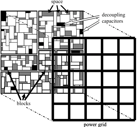
[image:2.595.313.533.510.714.2]A power grid model and block layer model are shown in Figure 1. The power grid formed the mesh has two-layer structure, the horizontal and the vertical layer. These layers are connected with vias. The power grid optimiza- tion is performed by not only changing power wiring width [4] but also insertion of decoupling capacitors. In- sertion of decoupling capacitors is effective for reducing IR-drop and inductor noise. Decoupling capacitors are placed in spare area in the block layer [3]. Block layer is mainly covered with standard cells. The ratio of the spare area is preset as the limitation which is able to place de- coupling capacitors. The chip area is not increased by insertion of the capacitors if they were placed in the spare area. However the optimization algorithm may require additional decoupling capacitors by increasing the block size. It is necessary to consider resulting in manufacturing cost increase.
3. Multi-Objective Optimization Flow
Power grid optimization is a multi-objective optimization problem. We want to optimize many objectives, IR drop, EM, chip area, wiring congestion and so on simultane-
ously. It is, generally, a very difficult problem. One rea- son is that each objective has different dimension. Sec- ond reason is that each of them has a different character- istic curve. We have introduced a new concept of risk functions to deal with those different characteristics at the natural process of the optimization schedule [6,7]. The risk function represents dangerous condition of LSI implementation by using 0% to 100%. Each objective is converted into the same dimension of risk using the risk function. The shape of the risk function should be care- fully defined. The combination of IR drop risk, EM, and wiring congestion risk is defined for each grid. Detail definition of the risk functions are stated in [7]. The risk value of the chip area is stated in this paper. The effec- tiveness is also shown in the section of experimental re- sults.
Figure 2 shows a flow of the power grid optimization. The optimization is scheduled with the gradient method. First, the power grid circuit is constructed with an RC network and initial values of the circuit elements are given (STEP 1). The dynamic current consumption of each functional blockis pre-determined by an RTL power simulation. It is represented as current sources connect- ing the power grid nodes of the corresponding area. Then, voltage and current of each nodes and edges are calcu- lated by dynamic circuit simulation (STEP 2). Next, a risk value of each grid is calculated (STEP 3). And the worst and four random grids are selected as the candi-dates of that they may be improved (STPE 4). Then for each candidate grid, the improvement operation i.e., change of power wiring width or insertion of decoupling capacitors, is examined (STEP 5). And a combination of selection of grids which has the highest value of the evalu- ation function is selected. If the value of the evaluation
power grid space
decoupling capacitors
blocks
power grid
decoupling capacitors space
space
decoupling capacitors
blocks blocks
No
Yes
Is the value of the evaluation function increased ? start
STEP5 : Evaluate design risks using evaluation function STEP4 : Pick up candidate grids
STEP3 : Calculate a risk value for each grid STEP2 : Run dynamic circuit simulation STEP1 : Construct RC network for power grid
[image:3.595.63.283.83.305.2]STEP6 : Update power grid end
Figure 2. Power grid optimization flow.
function is increased, the power grid by change of power wiring width and insertion of decoupling capacitors is updated (STEP 6). These operations are repeated as long as the value of the evaluation function is improved.
4. Risk Functions
4.1. Manufacturing Cost Risk Function
This chapter explains the relation between chip area and manufacturing cost. We begin with the definition of yield and critical area, and then we discuss about the manu- facturing cost risk. The calculation accuracy of manu- facturing cost has been increased by using exact critical area and by revealing the relation between critical area and chip area.
4.1.1. Yield
When chip area size increases, the number of chips pro- duced from one slice of wafer decreases. In addition, de- fective chips due to dust increase. Therefore, we consider a ratio of the number of the good chips which is produced by one slice of wafer. This ratio is called “yield”. The yield equation for LSI chip refers to [8,9]. Equation (1) is the yield function and Figure 3 shows the yield curve. The D0 is the average value of defect density in a unit area
and the Acr in the Equation (1) is size of critical area. We explain in detail by the following chapter.
0 cr D A Y e
maxmin d
x
cr x c
(1)
4.1.2. Critical Area
Critical area [9] is a layout area which has functional defects caused by particle contamination. Refer to Chap- ter 2 of [9] for a detailed account of the critical area. The
size of critical area is expressed by Equation (2).
A
A x f x x
(2)
The Acr is average value of the total of critical area, and it is calculated in critical area for all defect sizes. The Ac(x) is calculated in a critical area for defect size x. The f(x) is the defect size distribution function, and it is de-fined by Equation (3). The x0 is defined as a minimum
spacing in the design rule of LSI chip.
0 2
0 2 0
0 max 3
0
x if x x
x f x
x
if x x x x
(3)
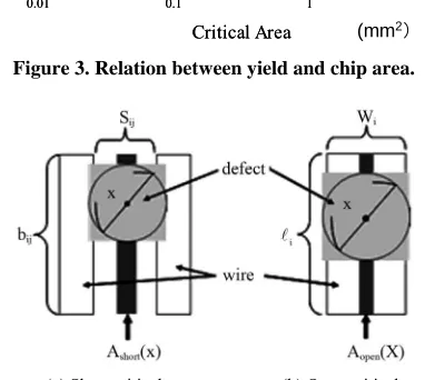
Critical area is defined by the sum of short critical area Ashortand open critical area Aopen,and is shown in
Equa-tion (4).
short
open( )c
A x A x A x (4) The Ac(x) of each defect size is calculated. Figure 4 shows a short and an open critical area. The functional failure by the short happens when defect size x exceeds the wiring spacing. And the functional failure by the open happens when defect size exceeds the wiring width. They are defined as Equations (5) and (6).
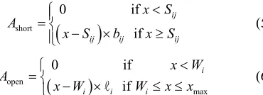
0.01 0.1 1 10 100
0.01 0.1 1 10
Critical Area
Yi
el
d,
Y
(mm2)
(%)
0.01 0.1 1 10 100
0.01 0.1 1 10
Critical Area
Yi
el
d,
Y
(mm2)
[image:3.595.314.530.372.724.2](%)
Figure 3. Relation between yield and chip area.
(a) Short critical area; (b) Open critical area
[image:3.595.315.530.420.595.2] [image:3.595.327.518.540.711.2]0 0.4 0.8 1.2 1.6 2
1 1.5 2 2.5 3 3.5 Chip Area C rit ical A rea ( A cr) (mm2)
(mm2)
0 0.4 0.8 1.2 1.6 2
1 1.5 2 2.5 3 3.5 Chip Area C rit ical A rea ( A cr) (mm2)
(mm2)
short 0 ij if i f ij ij ij x S Ax S b x S
max i i
(5)
x
open
0 if if
i i
W A
x W W
ℓ x x
(6)
An actual signal wire’s width and spacing are not uni-form. However, this paper’s purpose is the power grid optimization in consideration of manufacturing chip cost. Therefore, we define signal wires are arranged at equal interval, and the number of them is defined depending on the wire congestion in an area. Figure 5 shows the rela-tion between the chip area and the critical area calculated from signal wires that we defined temporarily. xmax of
Equation (2) used in this paper defined as a clean level of 0.12 μm.
Generally, if the chip area is only increased without re-design, spacing between the wires will be increased. Thus, critical area does not increase as same ratio as the area increase. It is observed from Figure 5 that if the chip area is increased three times, the critical area in-creases about two times. Thus, it is possible to more accurately estimate the chip area, and we can accurately estimate the manufacturing cost described in the next section.
4.1.3. Manufacturing Cost vs Chip Area
The more the chip area increases, the more the yield de-creases. The chip cost (=manufacturing cost) function can be represented by the Equation (7).
Costs W
Cost A a
W Y
A
(7)
In this Equation, A is a chip area, Y is a yield, WS is a wafer area, and WCost is a cost per one wafer. Here, the Y
is given by Equation (1). This is influenced by the critical area Acr. Also the Acr is influenced by the chip area A as shown in Figure 5. Thus, the Y is a function of A. The term WS/A×Y indicates the number of the good quality chips that can be manufactured from one wafer.
The basic cost of the chip is obtained by dividing the WCost by the term. The parameter a is a cost that does not
depends on the chip area. For example, the cost for test- ing and packaging are included in a. This cost value should be assigned depending on the circuit size and power consumption. The value is not so important for the discussions in this paper, and we set a relatively low cost 25 for a by assuming a low-power and low cost package for our experiment. Consequently the graph of the Equa- tion (7) is shown in Figure 6.
[image:4.595.96.281.86.153.2]We understand that chip costs increase at the same time when chip areas increase, and the area of the chip doesn’t necessarily increase because it may be arranged
Figure 5. Relation between chip area and critical area.
0 2000 4000 6000 8000 10000 12000
0 10 20 30 40 50 60 70
Chip area m an uf ac tur in g c os t
(mm2)
(¥) 0 2000 4000 6000 8000 10000 12000
0 10 20 30 40 50 60 70
Chip area m an uf ac tur in g c os t
(mm2)
(¥)
0
DC D D
A S S C C
Figure 6. Manufacturing cost and chip area.
in the space margin of the block, even if many decoup- ling capacitors are arranged. However the chip area in- creases when more decoupling capacitors are arranged than a certain number. Thus, the chip area is able to be represented by Equation (8).
(8)
The SDC is the size of a piece of decoupling capacitor, e.g., 0.05 mm × 0.05 mm, CD is the total number of de- coupling capacitors. The CD0 is the number of
decoup-ling capacitors filled into the space area. No area penalty is paid if the placed decoupling capacitors are less than
0 D
C . The S is initial chip area without decoupling ca-pacitors.
4.1.4. Manufacturing Cost Risk Definition
[image:4.595.312.536.86.233.2] [image:4.595.321.526.259.409.2]MAXcost is the border value.
cost R cost Cost 100 MAX A max P (9)4.2. Timing Error Risk Function
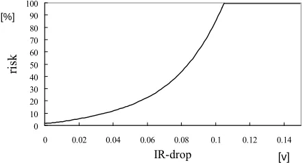
We have used the IR-drop risk function to eliminate the timing error caused by IR-drop. LSI’s functional blocks are constructed by a lot of transistors. To supply enough electrical power to the transistors is essential for desir- able operation of LSI because their operational speed degradation is caused by significant IR-drop. The low operational speed causes the timing error of the LSI. Hence, we have used “timing error risk function caused by IR drop” such as in Figure 7. This risk function de- fines the value of IR-drop in the horizontal axis and this risk value is defined as Rir.Details are explained in [7].
4.3. EM Risk Function
EM risk represents the danger of EM [6,7]. In super deep submicron technology, wire width of power grid be- comes more complicated and narrower, and power con- sumption of LSI becomes larger due to increased tran- sistors. The narrow wire tends to cut off by high current density so that larger current flows in the power grid. To design a chip which has high reliability, it is essential to eliminate the danger of EM, and so we have formulated EM risk function.
The EM risk function is defined the current density in a horizontal axis and the EM risk value is defined as Rem in the vertical axis. The EM risk is defined with the maxi- mum current density, σmax. The value of Rem is 100% when
current density is σmax. The value of Rem is defined 0%
when the current density is less than σp. The σp is shown in the Equation (10). The risk value between σmax and σp is used a linear function proportional to current density.
(10)
4.4. Wiring Risk Function
Wiring risk represents the danger of unwired failure on power grid. To optimize the power grid, we need to
0 10 20 30 40 50 60 70 80 90 100
0 0.02 0.04 0.06 0.08 0.1
IR-drop ri sk [%] 0.12 0.14 [v] 0 10 20 30 40 50 60 70 80 90 100
0 0.02 0.04 0.06 0.08 0.1
[image:5.595.62.283.601.720.2]IR-drop ri sk [%] 0.12 0.14 [v]
Figure 7. IR-drop Risk Function.
change wire width and insert decoupling capacitors. If the changed wire width is too wide, the LSI chip cannot be designed in desired chip area, and the power grid may become an unfeasible circuit [9]. Thus we have defined wiring risk function to get feasible power grid.
Each grid area includes power supply wires and signal wires. If a ratio of the total wiring area to the grid area increases, unconnected wire may occur. Sg is a grid area, Sp is an area that the power supply wires occupy, Sw is an area of the signal wires, and Wc formulated by Equation (11) represents a ratio of wiring area. The risk value is defined as Rrw. When the value of Wc is 0.2 or less, the risk value of Rrw is 0. When the value of Wc is 0.6 or more, this risk value of Rrw is defined as 100%.The risk value of Rrw between 0.2 and 0.6 is represented in shape similar to the EM risk. This function has been obtained by many experimental results.
p w c g S S W S
(11)4.5. Evaluation Function
We define new evaluation function which timing error due to IR-drop, EM, wiring congestion and chip cost are able to be all optimized simultaneously. If one of three risks, timing error, EM and wiring risks, becomes 100%, it is clear not to achieve feasible power grid. Hence we have defined a safety which a risk value is subtracted from 100. We have got a safe function by multiplication of three safeties from timing error, EM and wiring con- gestion. However, a safety value of manufacturing cost is changed by number of decoupling capacitors arranged in the entire chip. So we have not used manufacturing cost safety to evaluate each grid area. The safety function Safe(B) of a grid area B is shown as follows.
2
100 100 100
Safe
100
ir em rw
R R R
B (12)
Since Rir, Rem and Rrw are within 0% and 100%, Safe(B) is within 0% and 100%.
We define the evaluation function by a minimum safety value, the sum of safety value of all grids and safety value of manufacturing cost risk. A value of manufacturing cost risk is decided by the number of de- coupling capacitors arranged in the whole chip. And a value of cost risk is not derived in each grid. So the manufacturing cost element is not added in the safety function. Instead, we can add a safe degree of manufac- turing cost risk to the evaluation function because the evaluation function represents a safety of entire grid area.
Our evaluation function F(B)is defined as follows.
cost
min Safe
Safe 100
B
B
F B M B
B N R
The evaluation function F(B)consists of three of safe-ties. It is necessary to raise the minimum value of the safety of each grid in order to lead more safely for the entire power grid. The first term (1st safety) is the lowest safety in the entire power grid. The second term (2nd safety) is the total sum of the safety of each grid. A good solution cannot be obtained only by the 2nd safety. The 2nd safety is a role for preceding the optimization sched-ule smoothly. The reason why M is multiplied to the minimum Safe(B) is to improve a worst evaluated grid preferentially. Thus the M should be a big value to make the 1st safety bigger enough than the 2nd safety. The third tern (3rd safety) is the safety value of the manufac-turing cost risk.
The 1st safety and the 3rd safety decide the quality of optimization. That is, by controlling the M and N, it is possible to change the quality of the solution.When N is small enough compared with M, the safe value of the manufacturing cost reached almost to 0, and stop at the manufacturing cost limit.When N is gradually increased, the constraint of the manufacturing cost increases, and the safety of the electric and physical constraints (=1st safety) is slightly lower. Figure 8 shows a transition of each safety to M/N. The data used is 1.3 mm × 1.3 mm sized circuit data described in the next section.
As shown in Figure 8, N/M = 0.02 - 0.05 is the range which electrical and physical constraints are dominant because the manufacturing cost does not almost change. On the contrary, N/M = 0.12 is the range which the manufacturing cost constraints are dominant. When the adequate values of M and N are selected, tradeoff analy- sis is performed well, and it is considered to be able to reach better manufacturing cost result still keeping the good electric and physical conditions.
Figures 9-11 show transition of each safety to each M/N. Figure 10 shows an example when the tradeoff analysis is performed well. When the N is larger enough, only the cost optimization is performed as shown in Fig-ure 11. This is the case that we do not expect. We rather expect the case of Figure 9 or Figure 10 in general. These can be performed with less computation time of optimization. We may expect the case of Figure 10 op-timally. But it requires try and errors for selection of adequate M and N values to each LSI chip, and takes large computation time.
5. Experimental Results
We have applied to three different sized circuits to show the effectiveness of our proposal technique. N/M = 0.07 has used in Equation (13). The experiments are per- formed on P-4 processor with a speed of 3.4 GHz and 4 GB RAM. The program uses C language.
Figure 8. Transition of each safety to M/N.
Figure 9. Transition of each safety (N/M = 0.05).
Figure 10. Transition of each safety (N/M = 0.07).
The effects of safety improvement are shown in Table 1. In the table, “Average safety” is the average safety in the entire chip. IR-drop, EM, wiring and manufacturing cost have been all optimized in this experimentation.
[image:7.595.57.542.313.716.2]Although the processing time of CHIP 1 is 104 sec in Table 1, CHIP 3 reaches about 38 times longer than CHIP 1. There is room for improvement for the chip size.
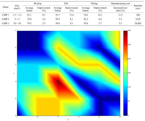
Risk distributions of the whole circuit before and after optimization for CHIP 1 are shown in Figure 13. From Figure 9, safe degree of EM comes up to the upper limit value soon after the optimization starts. IR-drop and EM risk values are noticeable at grids of both (1,1) and (6,6) in Figures 13(a) and (b). Because two power supply re- sources are connected to the points. They have no volt- age drop due to the power supply connections, but EM risk is high because a large current density flows there. The placement of decoupling capacitors has also the same tendency as EM in Figure 13(b). Not so many de-coupling capacitors are placed around the power supply resources, and the number of the capacitors increases on the area far away from the power sources.
For example, Transition of each safety for CHIP 1 is shown in Figure 10. Safety of the manufacturing cost has deteriorated from start to about ten times optimiza- tion because the priorities of IR-drop, EM and wiring are higher than the manufacturing cost. However, the safety of manufacturing cost is improved later and finally stabi- lized on about 100 times in this case. As a result, manu- facturing cost is slightly higher, but electrical constraints, IR-drop and EM are satisfied with all. The reason with sufficient electric constraints is an effect of insertion of decoupling capacitors. The distribution of decoupling capacitors placed on chip after the optimization of power grid is shown in Figure 12.
Table 1. Result of power grid optimization for 3 chips.
drop
-IR EM Wiring Manufacturing cost Size
(mm2) Average
Safety
Improvement (%)
Average Safety
Improvement (%)
Average Safety
Improvement (%)
Increased cost ratio (%)
Runtime
Name (sec)
CHIP 1 1.3 × 1.3 83.1 9.1 91.7 11.6 74.6 22.1 11.5 104 CHIP 2 5 × 5 79.8 3.6 99.5 0.1 43.2 6.8 3.5 2322 CHIP 3 10 × 10 79.5 5.5 99.9 0.1 39.8 5.7 5.5 38,403
[V]
(a) IR Drop
×105
[A/mm2]
(b) EM
[%]
[image:8.595.75.522.81.537.2](c) Wiring Congestion
Figure 13. Optimization results for CHIP 1.
6. Conclusion
We have proposed a methodology to optimize a power grid system in the floor plan for the physical design phase. Our approach can consider the risk of physical constraints and timing errors simultaneously, such as IR drop, EM and manufacturing cost. In particular, the manufacturing cost is calculated based on chip yield. In addition, since considering placement of decoupling ca- pacitance at the same time in the chip, power wiring strong against EM noise can be constructed. The experi- mental results have shown that power wiring optimiza- tion can be done while taking the balance of chip reli- ability and manufacturing cost. However, relatively large
chip such as the 10 × 10 mm2 will require longer proc-
essing time. A key issue for the future is speed up.
REFERENCES
[1] H. Su, K. H. Gala and S. S. Sapatnekar, “Fast Analysis and Optimization of Power/Ground Networks,” Interna-tional Conference on Computer Aided Design, San Jose, 5-9 November 2000, pp. 477-480.
doi:10.1109/ICCAD.2000.896518
[3] J. Fu, Z. Luo, X. Hong, Y. Cai, S. X.-D. Tan and Z. Pan, “A Fast Decoupling Capacitor Budgeting Algorithm for Robust On-Chip Power Delivery,” Proceedings of the Asia and South Pacific Design Automation Conference, Yokohama, 27-30 January 2004, pp. 505-510.
[4] T.-Y. Wang and C. C.-P. Chen, “Optimization of the Power/Ground Network Wire-Sizing and Spacing Based on Sequential Network Simplex Algorithm,” Proceedings of International Symposium on Quality Electronic Design, San Jose, 21 March 2002, pp. 157-162.
doi:10.1109/ISQED.2002.996721
[5] X. Wu, X. Hon, Y. Ca, C. K. Cheng, J. Gu and W. Dai, “Area Minimization of Power Distribution Network Us-ing Efficient Nonlinear ProgrammUs-ing Techniques,” In-ternational Conference on Computer Aided Design, San Jose, 4-8 November 2001, pp. 153-157.
[6] H. Ishijima, K. Kusano, T. Harada, Y. Kawakami and M.
Fukui, “An Algorithm for Power Grid Optimization Based on Dynamic Current Consumption,” International Association of Science and Technology for Development on Circuits, Signals and Systems, Vol. 531, 2006, pp. 114-119.
[7] Y. Kawakami, M. Terao, M. Fukui and S. Tsukiyama, “A Power Grid Optimization Algorithm by Observing Tim-ing Error Risk by IR Drop,” The IEICE Transactions on Fundamentals of Electronics, Communications and Com- puter Sciences, Vol. E91-A, No. 12, 2008, pp. 3423-3430. [8] The Institute of Electronics and Communication Engi-
neers, “LSI Handbook,” Ohmsha, 1984.