http://wrap.warwick.ac.uk
Original citation:Hassan, A. H. A., Morris, R. J. H. (Richard J. H.), Mironov, O. A., Beanland, Richard, Walker, David, 1978-, Huband, S., Dobbie, A. (Andrew), Myronov, Maksym and Leadley, D. R. (David R.). (2014) Anisotropy in the hole mobility measured along the [110] and [1¯10] orientations in a strained Ge quantum well. Applied Physics Letters, Volume 104 (Number 13). Article number 132108. ISSN 0003-6951
Permanent WRAP url:
http://wrap.warwick.ac.uk/60425
Copyright and reuse:
The Warwick Research Archive Portal (WRAP) makes this work of researchers of the University of Warwick available open access under the following conditions.
This article is made available under the Creative Commons Attribution 3.0 (CC BY 3.0) license and may be reused according to the conditions of the license. For more details see: http://creativecommons.org/licenses/by/3.0/
A note on versions:
The version presented in WRAP is the published version, or, version of record, and may be cited as it appears here.
Anisotropy in the hole mobility measured along the 110
½
and
½
110
orientations in a strained Ge quantum well
A. H. A. Hassan,a)R. J. H. Morris, O. A. Mironov,b)R. Beanland, D. Walker, S. Huband, A. Dobbie, M. Myronov, and D. R. Leadley
Department of Physics, University of Warwick Coventry, Coventry CV4 7AL, United Kingdom
(Received 9 January 2014; accepted 3 March 2014; published online 2 April 2014)
In this paper, we report on anisotropic transport properties of strained germanium (sGe) quantum wells grown on Si (001) substrates with p-type doping beneath the sGe channel. Mobility measurements were made along orthogonal [110] directions. The level of measured resistivity anisotropy in the 110½ and ½110 orientations was found to vary between 2 and 9 for different samples. This corresponds to an actual mobility anisotropy ratio of between 1.3 and 2, values that are significantly higher than previously found for sGe. From modeling of the low temperature (12 K) mobility, using the relaxation time approach, the anisotropy in mobility was accounted for by a difference in interface roughness scattering between the two orientations. For the 110½ orientation, a step height ofD¼0.28 nm and interface roughness periodicity ofk¼7 nm were found while for the ½110orientation, kreduced to 4 nm and Dincreased to 0.42 nm. High-resolution X-ray diffraction and transmission electron microscopy confirmed a 1off-cut in the wafer towards the½110direction.
VC 2014 Author(s). All article content, except where otherwise noted, is licensed under a Creative
Commons Attribution 3.0 Unported License.[http://dx.doi.org/10.1063/1.4870392]
Silicon remains the material of choice for many micro-electronic applications because of its abundance and low cost, and in order to keep advancing this technology platform, inno-vative solutions such as the incorporation of other materials have been sought. To improve the hole mobility Ge has been adopted because not only is it fully miscible with silicon but it also has a higher hole mobility. Furthermore, through con-trolled epitaxial growth, the lattice mismatch between Si and Ge can be exploited to introduce strain to the active layer. The introduction of strain results in a splitting of the heavy and light hole bands, which in turn leads to a reduction in the hole effective mass and the interband scattering.1 This has been shown to result in a further enhancement of the hole mobility,2 thereby offering significant performance improvement over current Si-based device technology.3 A common approach adopted for studying the transport properties of strained Ge (sGe) is through the epitaxial growth of a two-dimensional hole gas (2DHG) structure. Due to the large mismatch between Si and Ge (4.2%), a highly crystalline sGe layer of sufficient thickness to confine the carriers can only be realized if the sGe layer is grown on top of a Ge-rich Si1xGexbuffer layer. For this work, we used a relaxed Si0.2Ge0.8 buffer for which the valance band offset to the strained Ge is about 100 meV,1making it comparable to the conduction band off-set that was used in the strained silicon two-dimensional elec-tron gas (2DEG)4,5 structure that achieved a high electron mobility of 2106cm2V1s1.
Transport properties of sGe quantum wells (QWs) have been reported for a number of different growth methods, e.g., low-energy plasma-enhanced chemical vapor deposition
(LEPE-CVD)6–8 and molecular beam epitaxy (MBE).9,10 From these growth methods, the highest low temperature Hall mobility for holes recorded was 1.2105cm2 V1s1 at 2 K,8while at room temperature it was 3100 cm2V1s1.11 Recently, the growth of a sGe QW by reduced pressure chemical vapor deposition (RP-CVD)12,13 has significantly improved on all previous results, with a hole Hall mobility of 1.1106cm2V1s1at a sheet density of 2.91011cm2 at 12 K reported for a “normal” structure (i.e., with doping above the channel). The main reasons given for the extremely high mobility found in this structure was the purity of the Ge channel (Si<0.01%) and the low level of background impur-ities in the channel.
In this paper, we report on a set of samples (11–284, 11–285, 11–286, 11–287, 11–288) that were grown at the same time and using the same system that produced the wa-fer (11–289) with the highest reported 2DHG mobility at low temperature.12 However, a significant difference between these samples and that of Ref. 12 is that the doping was placed below the sGe QW channel, i.e., they are “inverted” structures. The samples were grown using an ASM Epsilon 2000 RP-CVD reactor and consisted of a 100 mm diameter Si (001) substrate (10–20Xcm) on top of which was depos-ited a 2.1lm thick, relaxed Si0.2Ge0.8reverse linearly graded (RLG) buffer.14This strain tuning buffer15is grown without any chemical mechanical polishing (CMP) and previously found to have a low threading dislocation density (TDD) of4106cm2.14,16On top of the RLG buffer, a B-doped supply layer, an undoped Si0.2Ge0.8spacer layer and then the sGe QW were grown, followed by another undoped Si0.2Ge0.8 layer and finally a thin Si cap. The Ge QW was confirmed to be fully strained for all the samples by high resolution X-ray diffraction (HR-XRD) reciprocal space mapping (strain is 0.65%60.01%). The QW width, spacer layer thickness, and doping level were varied within the sample set as set out in TableI.
a)
Also at Department of Physics, Tripoli University, Libya. Electronic addresses: [email protected], [email protected].
b)Also at International Laboratory of High Magnetic Fields and Low
Temperatures, Gajowicka 95, 53-421 Wroclaw, Poland. Electronic addresses: [email protected] and [email protected].
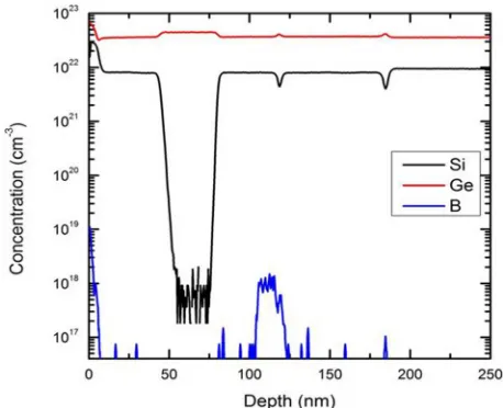
The structural properties of all the samples were studied by ultra-low energy secondary ion mass spectrometry (uleSIMS) using a near normal incidence O2þprimary beam at 250 eV (Figure 1, typical profile), HR-XRD using a Panalytical X’Pert Pro MRD diffractometer equipped with a hybrid monochromator giving pure CuKa1radiation in triple axis configuration, and cross-sectional transmission electron microscopy (XTEM) (Figure2, typical image). All the layer thicknesses were determined by both XTEM and uleSIMS and found to be in excellent agreement while the average B doping concentration was obtained from uleSIMS. Table I
summarizes all the values determined. The background B impurity levels elsewhere in the structure were below 1017cm3, as determined by the uleSIMS detection limit (From the previous SIMS measurements, with a lower noise floor, on material grown in this epitaxy system that used the same strain tuning buffer we believe the background impu-rity density to actually be below 1015cm3). Furthermore, the uleSIMS measurements also indicate that the Si concen-tration at the center of the sGe channel was in the range of 0.01–0.1 at. %, confirming that the low temperature (400C) epitaxy approach used here had achieved a high purity sGe
channel with minimal Si penetration to the sGe channel. The quality of the sGe interfaces also showed minimal roughen-ing (<1 nm) as indicated by the XTEM imaging and is best observed from the compressed version of the image shown on the right of Figure2.
For the transport measurements, Van der Pauw (VdP) structures were produced using wet chemical etching. Al contacts were deposited on the corners of the square samples (44 mm) by thermal evaporation and then annealed at 425C for 20 min under dry N2 to ensure ohmic behavior. Resistivity and Hall measurements were performed on all the samples over the temperature range of 12–300 K at a mag-netic field of 0.6 T for current flow in the two perpendicular surface directions, i.e., 110½ and½110, to study the anisot-ropy in the 2D-hole mobility
[image:3.612.51.562.77.242.2]The ratio of resistances measured in perpendicular direc-tions from a VdP sample overestimates the actual resistivity anisotropy for two reasons: first due to geometrical effects of the actual sample shape and positioning of the contacts and second, after correcting for geometry, an anisotropic resist-ance will alter the current flow and electric field distribution in the sample. The full analysis of this was provided by Bierwagen,17 and also mentioned recently by Martin,18 which allows us to convert the measured resistance ratio to a
TABLE I. Measured hole density (ps) and mobility at 12 K, for both the½110and 110½ orientations, along with layer thicknesses taken from uleSIMS
meas-urements (or XTEM where indicated).
Layer thickness (nm)
Sample Orientation ps1011cm2 Mobility105cm2/V s Channel Spacer Doping layer Doping density1017cm3
11–284 ½110 5.03 2.47 2262 (XTEM) 2062 1863 763 110
½ 3.36
11–285 ½110 6.90 2.74 1562 (XTEM) 2662 1263 963 110
½ 3.57
11–286 ½110 6.75 2.65 3862 (XTEM) 2062 2163 963 110
½ 3.48
11–287 ½110 7.89 1.12 2262 1262 1963 1063 110
½ 2.15
11–288 ½110 6.51 1.77 2062 2462 1563 1863 110
[image:3.612.59.288.555.741.2]½ 2.81
FIG. 1. uleSIMS depth profile showing the B, Si, and Ge distribution within sample 11–286.
FIG. 2. XTEM image for the sample 11–286 with a 10compression of the image on the right side to help show up any interface roughness.
[image:3.612.323.553.576.741.2]mobility anisotropy. The measured anisotropy ratioAVdP is related to an effective resistance anisotropyAeffby
AVdP¼
X
n¼oddþ
nsinh ffiffiffiffiffiffiffiffiA1
ef f q pn 1 X
n¼oddþ
nsinh qffiffiffiffiffiffiffiffiAef fpn
1: (1)
For an anisotropy of less than 10, a satisfactory approxi-mation can be obtained with just the n¼1 terms and a look-up table to find Aeff. From this, the actual anisotropy coefficientA can be determined with a simple geometrical correctionA¼Aef f Ly=Lx
2
, whereLyandLxare the dis-tances between contacts in the orthogonal directions. Finally, the resistivity for both orientations can be defined as qxx¼qave
ffiffiffiffiffiffiffiffi
A1
p
, and qyy¼qave
ffiffiffi
A
p
, and the mobility calcu-lated using the measured Hall Coefficient. TableI summa-rizes the calculated 12 K VdP mobility and sheet density found for½110and 110½ orientations in all the samples.
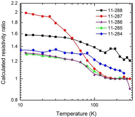
Significant anisotropy is observed in the mobility for temperatures below 100 K. However, at higher temperatures (100–300 K) this anisotropy almost disappears (1), although here parallel conduction dominates which may well mask any channel anisotropy that is not present in the paral-lel conduction layers. This was used as a check on the geom-etry of the samples; a correction was made for sample 11–288, but all the others hadA(300K) sufficiently close to
unity that no adjustments were made. The ratio of calculated sheet resistivity between the two directions, i.e., 110½ and ½110(Figure3), is found to be of the order 1.3 for the sam-ples 11–284, 11–285, and 11–286. For samsam-ples 11–288 and 11–287, this rises to 1.5 and 2, respectively, indicating a much stronger anisotropy in the sample which corresponds to the largest measured sheet density. For the asymmetric doping arrangement in our structures, Poissson-Schr€odinger simulation of the electrostatics shows that the hole wave-function is predominantly at the lower interface of the quan-tum well and this invariance of mobility suggests that even
for a 15 nm wide well the holes are not significantly affected by the other interface. We might expect that for thinner quantum wells there would be some reduction in mobility. For each sample, the same Hall coefficient value was observed for both orientations, which would be expected since the value of carrier density should be the same in whichever direction it is measured; however, this does con-firm that the measured mobility anisotropy is a consequence of different scattering rates in the two directions.
There are a number of scattering mechanism contribut-ing to the hole mobility. At high temperature, the dominant mechanism is expected to be phonon scattering,19 which should be isotropic; indeed the measured difference in resis-tivity vanishes above about 200 K. Ionized impurity scatter-ing is also isotropic; at low temperature and low carrier density, scattering from background impurities will be most important, with the influence of remote impurities (in the B-supply layer) increasing at higher hole density. The influ-ence of interface roughness scattering also increases with carrier density,20and roughness can vary with orientation. It is therefore reasonable to investigate whether interface roughness scattering is responsible for the anisotropy that we see increasing with hole density. Indeed a previous study on GaAs (Ref. 21) did attribute a mobility anisotropy that increased with sheet density to interface roughness or sub-strate off-cut.22–24We have therefore calculated the mobility contributions from these various scattering mechanisms to compare with the experimental values. We used the relaxa-tion time approach to calculate the remote impurity scatter-ing rate as25–28
1 sRI
¼ e
4mn
i
8ph3e2q3
F
ðp
0
eð4qðLsþwÞsinhÞsinh
sinhþS0=2qF
ð Þ2 dh; (2)
whereniis the remote ionized impurity density,eis the elec-tron charge, m* is the effective mass of the holes which is assumed to be isotropic in our samples because a similar level of strain was found for both orientations by HR-XRD. The effective mass value used in this study was 0.07 m0 which had been extracted previously using magnetotransport measurements of 11–284,13qFis the Fermi wave vector,Ls is the spacer thickness,wis the channel thickness, andS0is the screening constant.26
For background impurity scattering we have27,28
1 sBI
¼ e
4
mNB 8ph3e2q2
F
ðp
0
sinhð1e2qFsinhÞ
sinhþS0=2qF
ð Þ2 dh; (3)
whereNBis the two-dimensional background impurity den-sity in the QW.
Finally, the relaxation time for interface roughness scat-tering is given by29
1 sIR
¼e
4mD2
K2
h3e2 NDeplþ
ps 2
2
eq 2K2
4 ; (4)
[image:4.612.60.291.543.743.2]where the hole sheet density ps and NDepl determine the effective normal electric field in the channel. D parameter-izes the interface roughness height, and K is the interface roughness correlation length, in the direction being
considered. We note that, whilstDandKare related to phys-ical dimensions in the sample, they are treated as variable pa-rameters in the modeling.
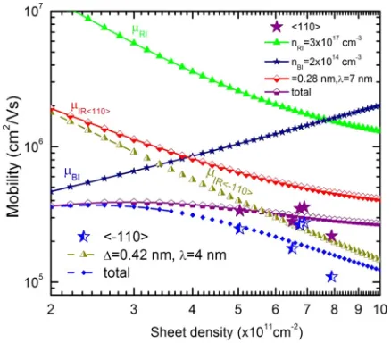
Figure 4 shows the best agreement found with our calculated mobilities along with the parameters used to obtain this. According to our simulations, the best fit for both orientations was achieved for a remote ionized impurity level of 31017cm3 and background impurity level of 21014cm3. Although the latter is well below the SIMS detection threshold, it is a realistic value that is consistent with estimates of the residual impurity levels from, for instance, dark-count measurements in Ge detectors grown in the same system. It is also slightly greater than the value of 51013cm3 that we needed to use in simulations30 that reproduce the higher measured mobility in the normal struc-ture of Ref.12. In the 110½ orientation, an interface roughness height of D¼0.28 nm with interface roughness periodicity K¼7 nm was found. For the½110orientation, the roughness height D increased to 0.42 nm and the correlation length K had to be reduced (4 nm). These findings indicate that the large mobility anisotropy observed arises from a monolayer roughness (up to3 monolayers) that has a nm-scale perio-dicity, possibly due to the (001) Si substrate off-cut leading to a step like structure for the½110direction.22–24
Although the initial XTEM measurements (shown in Figure2) do not reveal any interface roughness in our struc-tures, anything below about 1 nm would not be obvious in the images. Further high-resolution XTEM images were obtained using an aberration corrected microscope that do appear to show a significant difference in off-cut angle between the two orientations, i.e.,h110iandh110iof up to 1 (see Table II). (The values reported are averages of at least three measurements per sample direction with an uncertainty of60.3 coming from the spread in measured
slopes.) The orientation of the wafers was also measured by HR-XRD. Accurate positions of the (224), (044), and (004) reflections were determined and hence the misorientation of the wafer relative to the goniometer could be found via an orientation matrix. This enabled the relative off-cut in 110½
and½110directions to be calculated to60.1 (TableII). Both measurement techniques agree that there is about a 1off-cut towards ½110. This difference in off-cut angle will affect both the terrace height and length and hence the scattering rates in the two orthogonal directions.
In conclusion, significant mobility (resistivity) anisot-ropy between 110½ and½110orientations has been found in sGe quantum well structures. The anisotropy coefficient determined was between 1.3 and 2. Using the relaxation time approximation for isotropic remote impurity scattering, background impurity scattering, and anisotropic interface roughness scattering, it was found that the difference in mo-bility could be modeled by varying the interface roughening scattering parameters between the two orientations. For the
110
½ direction, an interface roughness height ofD¼0.28 nm with interface roughness periodicityK¼7 nm was found but for the ½110 orientation a larger roughness height (D¼0.42 nm) and shorter periodicity (K¼4 nm) were found, indicating a larger interface roughness effect was affecting the mobility in the ½110 direction. HR-XRD and XTEM results appear to indicate this interface roughness variation is from a 1 difference in off-cut angle between
110
½ and½110orientations which may arise from the start-ing (001) Si substrate.
This work was partially supported by EPSRC projects EP/F031408/1 and EP/J001074/1; the Slovak Research and Development Agency under Contract Nos. APVV-0132-11 and VEGA-0106-13, and SAS Centre of Excellence CFNT MVEP (Kosice, Slovakia). OAM acknowledges the National Scholarship Program of the Slovak Republic for the Mobility Support for Researchers the Academic Year 2012/2013. The Panalytical MRD diffractometer used was obtained through the Science City Advanced Materials Project, with support from Advantage West Midlands and part funded by the European Regional Development Fund.
1
F. Schaffler,Semicond. Sci. Technol.12(12), 1515–1549 (1997).
2
K. Sawano, H. Satoh, Y. Kunishi, K. Nakagawa, and Y. Shiraki,
Semicond. Sci. Technol.22(1), S161–S163 (2007).
3S. M. Sze,Physics of Semiconductor Devices, 2nd ed. (Wiley, New York,
1981).
4
T. M. Lu, C.-H. Lee, S.-H. Huang, D. C. Tsui, and C. W. Liu,Appl. Phys. Lett.99(15), 153510 (2011).
5S.-H. Huang, T.-M. Lu, S.-C. Lu, C.-H. Lee, C. W. Liu and D. C. Tsui, Appl. Phys. Lett.101(4), 042111 (2012).
6
H. von Kanel, D. Chrastina, B. Rossner, G. Isella, J. P. Hague, and M. Bollani,Microelectron. Eng.76(1-4), 279–284 (2004).
[image:5.612.315.562.77.171.2]7H. von Kanel, M. Kummer, G. Isella, E. Muller, and T. Hackbarth,Appl. Phys. Lett.80(16), 2922–2924 (2002).
FIG. 4. Mobility simulation for the (½110and 110½ ) orientations taking into account remote impurity scattering, background impurity scattering, and interface roughness.
TABLE II. Substrate off-cut angle determined from XRD and HR-TEM for orthogonal directions.
Si substrate off-cut angle
Sample Orientation (XRD) (XTEM)
11–287 ½110 1.160.1 1.560.3
11–287 ½110 0.160.1 0.360.2
11–288 ½110 1.060.1 0.960.6
11–288 ½110 0.260.1 0.460.2
[image:5.612.65.284.543.735.2]8B. Rossner, D. Chrastina, G. Isella, and H. von Kanel,Appl. Phys. Lett.
84(16), 3058–3060 (2004).
9
T. Irisawa, H. Miura, T. Ueno, and Y. Shiraki,Jpn. J. Appl. Phys., Part 1
40(4B), 2694–2696 (2001).
10M. Myronov, T. Irisawa, O. A. Mironov, S. Koh, Y. Shiraki, T. E. Whall,
and E. H. C. Parker,Appl. Phys. Lett.80(17), 3117–3119 (2002).
11
M. Myronov, K. Sawano, Y. Shiraki, T. Mouri, and K. M. Itoh, Appl. Phys. Lett.91(8), 082108 (2007).
12
A. Dobbie, M. Myronov, R. J. H. Morris, A. H. A. Hassan, M. J. Prest, V. A. Shah, E. H. C. Parker, T. E. Whall, and D. R. Leadley, Appl. Phys. Lett.101(17), 172108 (2012).
13A. H. A. Hassan, O. A. Mironov, A. Feher, E. Cizmar, S. Gabani, R. J. H.
Morris, A. Dobbie, V. A. Shah, M. Myronov, L. B. Berkutoy, V. V. Andrieyskii, and D. R. Leadley, in International Conference on Ultimate Integration on Silicon (ULIS-14), Warwick, March 2013.
14V. A. Shah, A. Dobbie, M. Myronov, D. J. F. Fulgoni, L. J. Nash, and
D. R. Leadley,Appl. Phys. Lett.93(19), 192103 (2008).
15
M. Myronov, A. Dobbie, V. A. Shah, X. C. Liu, V. H. Nguyen, and D. R. Leadley, Electrochem. Solid State Lett. 13(11), H388–H390 (2010).
16V. A. Shah, A. Dobbie, M. Myronov, and D. R. Leadley,J. Appl. Phys.
107(6), 064304 (2010).
17
O. Bierwagen, R. Pomraenke, S. Eilers, and W. T. Masselink,Phys. Rev. B
70(16), 165307 (2004).
18N. Martin, J. Sauget, and T. Nyberg,Mater. Lett.
105(0), 20–23 (2013).
19
A. M. Savin, C. B. Soerensen, O. P. Hansen, N. Y. Minina, and M. Henini,
Semicond. Sci. Technol.14(7), 632 (1999).
20T. Ando, A. B. Fowler, and F. Stern,Rev. Mod. Phys. 54(2), 437–672
(1982).
21
Y. Markus, U. Meirav, H. Shtrikman, and B. Laikhtman,Semicond. Sci. Technol.9(7), 1297 (1994).
22R. Neumann, K. Brunner, and G. Abstreiter,Physica E13(2–4), 986–989
(2002).
23
R. Neumann, J. Zhu, K. Brunner, and G. Abstreiter, Thin Solid Films
380(1–2), 124–126 (2000).
24H. Lichtenberger, M. M€uhlberger, C. Schelling, and F. Sch€affler,J. Cryst. Growth278(1–4), 78–82 (2005).
25
C. J. Emeleus, T. E. Whall, D. W. Smith, R. A. Kubiak, E. H. C. Parker, and M. J. Kearney,J. Appl. Phys.73(8), 3852–3856 (1993).
26K. Lee, M. S. Shur, T. J. Drummond, and H. Morkoc, J. Appl. Phys.
54(11), 6432–6438 (1983).
27
J. Lee, H. N. Spector, and V. K. Arora,J. Appl. Phys.54(12), 6995–7004 (1983).
28K. Hess,Appl. Phys. Lett.35(7), 484–486 (1979).
29D. Monroe, Y. H. Xie, E. A. Fitzgerald, P. J. Silverman, and G. P. Watson, J. Vac. Sci. Technol., B11(4), 1731–1737 (1993).
30