Original citation:
Beltran, A. M., Ben, T., Sanchez, A. M., Gass, M. H., Taboada, A. G., Ripalda, J. M. and Molina, S. I.. (2013) Compositional analysis of InAs-GaAs-GaSb heterostructures by low-loss electron energy loss spectroscopy. Journal of Physics: Conference Series, Volume 471 . Article number 012012.
Permanent WRAP url:
http://wrap.warwick.ac.uk/59296
Copyright and reuse:
The Warwick Research Archive Portal (WRAP) makes this work of researchers of the University of Warwick available open access under the following conditions.
This article is made available under the Creative Commons Attribution- 3.0 Unported (CC BY 3.0) license and may be reused according to the conditions of the license. For more details seehttp://creativecommons.org/licenses/by/3.0/
A note on versions:
The version presented in WRAP is the published version, or, version of record, and may be cited as it appears here.
This content has been downloaded from IOPscience. Please scroll down to see the full text.
Download details:
IP Address: 137.205.202.97
This content was downloaded on 31/01/2014 at 15:13
Please note that terms and conditions apply.
Compositional analysis of InAs-GaAs-GaSb heterostructures by Low-Loss Electron Energy
Loss Spectroscopy
View the table of contents for this issue, or go to the journal homepage for more
Home Search Collections Journals About Contact us My IOPscience
Compositional analysis of InAs-GaAs-GaSb heterostructures
by Low-Loss Electron Energy Loss Spectroscopy
A M Beltrán1,5,6, T Ben1, A M Sánchez2, M H Gass3, A G Taboada4, J M Ripalda4 and S I Molina1
1
Departamento de Ciencia de los Materiales e I.M. y Q.I., Facultad de Ciencias, Universidad de Cádiz, Campus Río San Pedro, s/n, 11510 Puerto Real, Cádiz, Spain
2
Physics Department, University of Warwick, Coventry CV4 7AL, United Kingdom
3
UK SuperSTEM, Daresbury Laboratory, Daresbury WA4 4AD, United Kingdom
4
Instituto de Microelectrónica de Madrid (CNM, CSIC), Isaac Newton 8, 28760 Tres Cantos, Madrid, Spain
E-mail: [email protected]
Abstract. As an alternative to Core-Loss Electron Energy Loss Spectroscopy, Low-Loss EELS is suitable for compositional analysis of complex heterostructures, such as the InAs-GaAs-GaSb system, since in this energy range the edges corresponding to these elements are better defined than in Core-Loss. Furthermore, the analysis of the bulk plasmon peak, which is present in this energy range, also provides information about the composition. In this work, compositional information in an InAs-GaAs-GaSb heterostructure has been obtained from Low-Loss EEL spectra.
1.Introduction
Self-assembled InAs(Sb)GaAs quantum dots (QDs) heterostructures have received much attention since they are able to emit at 1.3-1.55 µm even at room temperature [1,2]. This emission range is useful for telecommunication lasers and opto-electronic applications. Since opto-electronic properties depend on the structural quality and compositional distribution, their full characterization is essential to establish a relationship among structure, real composition and properties.
Compositional distribution can differ from the nominal one due to the concurrence of different effects during the epitaxial growth such as segregation and surface diffusion [3,4]. In fact, previous Scanning-Transmission Electron Microscopy (STEM) studies of InAs QDs grown by Molecular Beam Epitaxy (MBE) over a GaAs (001) substrate suggest the formation of the InxGa1-xAsySb1-y alloy when a
GaSb layer is directly grown on the QDs [5]. These compositional changes are very important for the application and production of QDs. This emphasizes the importance of very high resolution analytical techniques for the study of these heterostructures in order to understand the origin of the inherent decompositions and contribute to their improvement.
Classical analytical transmission and/or scanning transmission electron microscope techniques, such as Energy Dispersive X-Ray (EDX) and Electron Energy Loss Spectroscopy (EELS), are not
5
Present address:Center for Nanoanalysis and Electron Microscopy (CENEM). Department
Werkstoffwissenschaften, Universität Erlangen-Nürnberg, Cauerstrasse 6, 91058, Erlangen, Germany
6
To whom any correspondence should be addressed
useful for analysing In-Ga-As-Sb heterostructures due to overlapping signals associated with several elements. As an alternative, Low-Loss EELS is a suitable method for the analysis of these systems since in this energy range (0-60 eV), the edges corresponding to these elements are better defined. Besides, the bulk plasmon peak is also present in this range, providing additional information about compositional distribution and strain of the heterostructures [6]. In this work, compositional distribution of an InAs-GaAs-GaSb QDs heterostructure is estimated by the analysis of Low-Loss EEL spectra.
2.Experimental details
The studied heterostructure consists of 2.2 ML of InAs QDs grown by MBE at 510ºC on a GaAs (001) substrate. QDs have been capped by 6 ML of GaAs intermediate layer at 480°C, followed by 3 ML of GaSb and 100 nm of GaAs grown at 590ºC. Electron-transparent TEM samples were prepared following classical methods of mechanical grinding, dimpling and Ar milling at low voltage to minimize the damage. Only the thinnest areas of the sample (30-35 nm) were analysed to avoid the broadening and the shift of the plasmon peak due to surface excitation.
Spectrum Images (SI) have been acquired in SuperSTEM-1 (Daresbury Lab, U.K.), a VG HB501 UX FEG STEM equipped with a Nion spherical aberration corrector operating at 100 kV and a Gatan ENFINA™ parallel electron energy loss spectrometer system. The nominal probe size is 0.13 nm. The EELS data were acquired, from 0 to 60 eV, using a collection aperture with a semi-angle of 5 mrad and a convergence semi-angle of 24 mrad. A typical EELS map contained 700 spectra. The acquisition time for each spectrum was 0.35 s. In the Low-Loss region of the spectrum, using an energy dispersion of 0.05 eV per channel, the reached energy resolution was 0.35 eV. Although the use of a microscope with very small probe size allows a precise estimation of the composition, a 10% of error is expected. Apart from SI, high angle annular dark field (HAADF) images before and after the spectrum acquisition have been recorded to check the drift and/or damage caused in the sample by the beam, which have been negligible.
To analyse a SI, Zero-Loss peak and plural scattering must be removed using a standard Fourier-log deconvolution routine to obtain the Single Scattering Distribution which is related to the energy-loss function and contains the plasmon peak and the edges corresponding to the M and N signals. Then, the Kramers-Kronig (K-K) transformation is applied over the SSD to obtain the energetic dependence of the real, ε1, and imaginary, ε2, parts of the dielectric function. We will focus
on the imaginary part, because it contains information of the 3d and 4d transitions. These main signals are 3d transitions for As (M4,5 ~41 eV) and Ga (M4,5 ~20-22 eV) and 4d for In (N4,5 ~18 eV) and Sb
(N4,5 ~31 eV) [6]. After the background removal, signals have been integrated with a range of around
0.5 eV each side, to minimize the contribution of other near-by signals
The bulk plasmon peak is one of the most important signals in the Low-Loss region and it is the collective oscillation of the loosely bound electrons. Its shape and energy are characteristic of each solid. It can be simply described by the Drude-Lorentz model [7] which includes the single damped harmonic oscillator energy and the dielectric function of the core electrons. The bulk plasmon peak is modified by compositional and/or strain variations, even by the thickness of the TEM sample, among other factors. It has been observed that the change in the electron density via lattice parameter is the dominating factor determining the shift of the plasmon peak, where changes due to the band structure are a second-order effect. A full description of the methodology, including the relation among the parameters, as the lattice and the core dielectric constants can be found in reference [8].
3. Results and discussion
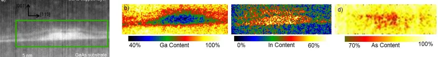
EEL spectra were acquired from the green rectangle marked in the HAADF of a QD (Figure 1a). After checking that the drift is reduced, steps described in the previous section have been followed to extract the imaginary part of the dielectric function. Then, the background is removed and signals are integrated over a range of ±2 eV. Extracted compositional maps are shown in Figures 1b)-1d).
18th Microscopy of Semiconducting Materials Conference (MSM XVIII) IOP Publishing Journal of Physics: Conference Series 471 (2013) 012012 doi:10.1088/1742-6596/471/1/012012
Considering the complementary relationships between composition of groups III and V, from the compositional map of Ga and As, the distribution of In and Sb could be estimated as CIn=100-CGa
and CSb=100-CAs where CIn, CGa, CSb and CAs represent In, Ga, Sb and As concentrations, respectively.
[image:5.595.74.520.262.320.2]Ga and As elemental maps are normalized with respect to Ga and As signals from GaAs substrate. The maximum of Ga is located on the substrate and surrounding the QD (Figure 1b). Inside the QD, Ga content is around 40% due to the well-known segregation phenomenon in InGaAs QDs systems [15]. Following a similar estimation procedure, As concentration inside the QD is estimated over 75-80%. Therefore, As is partially replaced by Sb. The Sb signal has been also extracted but, due to the high segregation coefficient of Sb and considering the inherent error of this analytical technique (around 10%) its content is expected to be below the error limit, which has been already confirmed by the analysis of this and similar heterostructures by other advanced techniques [9].
Figure 1. a) HAADF image of the studied heterostructure, showing a QD in the growth direction. The observed vertical stripes are due to the scan of the microscope. b), c) and d) show the Ga, In and As maps, respectively, corresponding to the green colour marked area on Figure 1a).
Furthermore, Ga and In elemental profiles have been acquired along the grown direction in a bi-dimensional area between QDs and integrated across the interface, in order to increase the signal/noise ratio (Figure 2). Maxima of Ga at the beginning and at the end of the profile are observed, corresponding to the GaAs substrate and final GaAs layer, respectively. After the first Ga maximum, there is a minimum on the Ga profile which corresponds to a maximum In content (InAs wetting layer). There should also be another Ga-maximum (from the GaAs intermediate layer) but instead, there is a relative maximum Ga peak, indicating a modification of the composition from the nominal one. It is followed by a relative minimum before the final maximum value. In every case, a Ga concentration decrease corresponds with an In increase, which confirms the complementarity of both elements, as we can observe even at the end of the analysed area; in this area it is more difficult to appreciate this behaviour due to the intensity decrease of the EEL signal. Although the existence of an In segregation process in these heterostructures is well-known, this profile does not correspond to a typical one in which, after a maximum, the In concentration decreases along the GaAs intermediate layer [10]. Instead, two In peaks are observed due to the presence of segregated Sb from the GaSb layer, which strongly competes with In and effectively blocks its incorporation into the lattice [9].
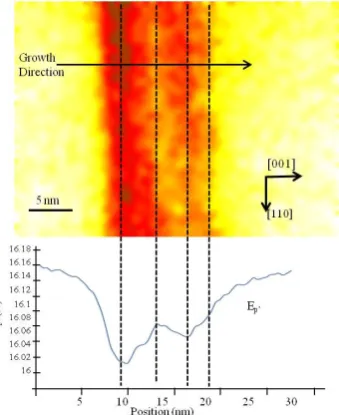
Concerning the bulk plasmon signal, bi-dimensional areas between QDs have been analysed. Figure 3 shows the variation of the plasmon energy Ep’, determined by a Gaussian fit,along the growth
direction and integrated across the interface. For a GaAs-based heterostructure, the bulk plasmon is located around 16 eV; the observed shift is due to the relationship between plasmon energy and electron density, which is represented through the variation of the lattice volume. Changes of the plasmon energy are mainly originated by differences of the unit-cell size [11]. Ep’ moves to low
energetic values with respect to GaAs, following a tendency similar to the experimental Ga profile taken from a Low-Loss EELS (Figures 2 and 3). Therefore, even when the slight variations of Ep’
Figure 2. a) HAADF image of a bi-dimensional area. b) and c) represent Ga and In elemental distribution profiles, respectively.
Figure 3. Image of the plasmon peak map and Ep’ profile integrated signal from a Low-Loss
spectra.
4. Conclusions
Low-Loss EELS is an alternative method for compositional analysis of quaternary semiconductor heterostructures for alloys with convoluted core-loss peaks. Analyses show the existence of In-Ga atomic intermixing in the studied In-Ga-As-Sb heterostructure. Specifically, the formation of InxGa1-xAs and InxGa1-xSbyAs1-y alloys has been detected because of In segregation in spite of the
presence of 6 ML GaAs intermediate layer.
Acknowledgements
This work was supported by the Spanish MINECO (project TEC2011-29120-C05-03 and CSD2009-00013) and the Junta de Andalucía (TEP-120 and INNANOMAT TEP-946 PAI research groups). Co-financing from UE-FEDER is also acknowledged.
References
[1] Akahane K, Yamamoto N and Ohtani N 2004 Phys. E21 295
[2] Ripalda J M, Granados D, González Y, Sánchez A M, Molina S I and García J M 2005 Appl. Phys. Lett.87 202108
[3] Moison J M, Houzay F, Barthe F, Gerard J M, Jusserand B, Massies J and Turco-Sandroff F S 1991 J. Cryst. Growth111 141
[4] Taboada A G et al 2010 Phys. Rev. B82 235316 [5] Molina S I et al 2007 Appl. Phys. Lett.91 263105
[6] Egerton R F 1996 EELS in the electron microscope (New York Plenum Press)
[7] Ahn C C 2004 Transmission electron energy loss spectrometry in materials science and the EELS atlas (California Wiley VCH)
[8] Sánchez A M, Beanland R, Papworth A J, Goodhew P J and Gass M H 2006 Appl. Phys. Lett.
88 051917
[9] Sánchez A M , Beltrán A M, Beanland R, Ben T, Gass M H, De la Pegna F, Walls M, Taboada A G, Ripalda J M and Molina S I 2010 Nanotechnology21 145606
[10] Muraki K, Fukatsu S and Shiraki Y 1992 Appl. Phys. Lett. 61 557
[11] Sánchez A M, Beanland R, Gass M H, Papworth A J, Goodhew P J and Hopkinson M 2005 Phys. Rev. B72 075339
18th Microscopy of Semiconducting Materials Conference (MSM XVIII) IOP Publishing Journal of Physics: Conference Series 471 (2013) 012012 doi:10.1088/1742-6596/471/1/012012
[image:6.595.314.484.113.321.2]