warwick.ac.uk/lib-publications
A Thesis Submitted for the Degree of PhD at the University of Warwick
Permanent WRAP URL:
http://wrap.warwick.ac.uk/95085
Copyright and reuse:
This thesis is made available online and is protected by original copyright. Please scroll down to view the document itself.
Please refer to the repository record for this item for information to help you to cite it. Our policy information is available from the repository home page.
First-Principles Simulation of Functional
Materials Interfaces
by
Ebiyibo Collins Ouserigha
Thesis
Submitted to the University of Warwick
for the degree of
Doctor of Philosophy
Department of Physics
Contents
List of Tables iv
Acknowledgments vi
Declarations vii
Abstract x
Chapter 1 Introduction 1
1.1 Overview . . . 1
1.2 Structures of the Transition Metal Pnictide MnSb . . . 4
1.3 Half-Metals . . . 5
1.4 Electron Counting Rule for III-V Semiconductor Polar Surfaces 9 1.5 Organization of the Thesis . . . 13
Chapter 2 Theoretical Background 15 2.1 Density Functional Theory . . . 15
2.2 Generalized Gradient Approximation . . . 19
2.3 Hubbard U and DFT+U . . . 24
2.4 Plane waves and Pseudopotentials . . . 27
2.4.1 Plane-waves basis sets . . . 28
2.4.2 Pseudopotentials . . . 29
2.5 Broyden-Fletcher-Goldfarb-Shanno Scheme . . . 33
2.6 Computational Code and Softwares . . . 36
2.6.1 CASTEP Package . . . 36
Chapter 3 Half-metallicity of c-MnSb and c-MnSb/InSb(111)
interfaces 42
3.1 Introduction . . . 42
3.2 Computational Methods and Calculated bulk Properties . . . 43
3.3 c-MnSb(111)/InSb(111) superlattices . . . 49
3.4 Summary . . . 56
Chapter 4 Ferromagnetic n-MnSb on III-V Semiconductors 57 4.1 Introduction . . . 57
4.2 n-MnSb(0001)/InP(111) superlattices . . . 58
4.2.1 Model Preparation . . . 58
4.2.2 Results . . . 59
4.3 n-MnSb(0001)/GaAs(111) superlattices . . . 64
4.3.1 Model Preparation . . . 64
4.3.2 Results . . . 65
4.4 Summary . . . 68
Chapter 5 The Sb(0001)/n-MnSb(0001) superlattice 71 5.1 Introduction . . . 71
5.2 Models and Computational Method . . . 75
5.3 Results . . . 76
5.4 Summary . . . 81
Chapter 6 NiO/MgO heterostructures 82 6.1 Introduction . . . 82
6.2 NiO/MgO(111) . . . 85
6.2.1 Models and Computational Method . . . 85
6.2.2 Results . . . 85
6.3 NiO/MgO(001) . . . 92
6.3.1 Models and Computational Method . . . 92
6.3.2 Results . . . 92
6.4 NiO/MgO(110) . . . 96
6.4.1 Models and Computational Method . . . 96
6.4.2 Results . . . 98
List of Tables
1.1 Structural properties of the three polymorphs MnSb. . . 5
1.2 Illustration of electron counting for the (2×2) GaAs(111)A re-construction given in figure 1.6(a). . . 12
3.1 Lattice parameters (˚A) of InSb andc-MnSb. . . 45
3.2 The optimized bond length between the interfacial atoms, the
calculated work of separation and spin magnetic moment of the
interface Mn atom for the four considered configurations of the
c-MnSb/InSb (111) interfaces. An asterisk (∗) indicates the magnetic moment for cases where the Mn atom is located in the subinterface layer. . . 51
4.1 The optimized bond length (L) between the interfacial atoms
and the calculated work of separation (W) for the various
in-terface ordering studied. (the inin-terface order Mn-P is spin
po-larized and more stable than others). . . 60
4.2 Spin polarization P and magnetic moments µ in µB at the n
-MnSb(0001)/InP(111) interfaces for the first two layers of n
-MnSb and InP slabs from the interface, for the four termina-tions. An asterisk (*) denotes atoms in the second atomic layer
of InP slab. . . 62
4.3 Interfacial bond length (L) and work of separation (W) for the
4.4 Spin polarization P and magnetic moments µ in µB at the n
-MnSb(0001)/GaAs(111) interfaces for the first two layers of n
-MnSb and GaAs slabs from the interface, for the four
termina-tions. An asterisk (*) denotes atoms in the second atomic layer
of GaAs slab. . . 68
5.1 Growth conditions for Sb/MnSb heterostructures. The Sb cap
layer was deposited for 90 s while cooling from 250 to 230 ◦C.
And the flux (JSb/M n) was not measured between the Sb cap
and MnSb(2) layer. . . 72 5.2 Measuredalattice parameters of the films grown compared with
their bulk values. The films a lattice parameters are computed
from GaAs scaling. . . 74
5.3 The optimized bond length (L) between the interfacial atoms,
the calculated work of separation (WR) for the various interface
ordering studied and there average magnetic moments. . . 79
5.4 Interfacial separation for the n-MnSb/Sb(0001) interfaces, and
given in brackets are changes in percentage of the interlayers. . 79
6.1 Comparison of the computed lattice parameters and band gap for MgO and NiO with previous works. . . 84
6.2 The calculated work of separation (WR) for the various interface
ordering studied, there optimized bond length (L) between the
interfacial atoms, and the interlayer distances (d). . . 86
6.3 The calculated work of separation (WR), interlayer distances
and optimized bond length (L) between the interfacial atoms
for the various interface ordering studied. . . 94
6.4 The calculated work of separation (W) and interlayer distances
Acknowledgments
I will like to thank my supervisor Dr. Gavin R. Bell for giving me the
oppor-tunity to work under him and for being very supportive of my research work.
Niger Delta University, Wilberforce Island, Nigeria, gave me the opportunity
to go on a Study Leave and supported my studies, which I am grateful for.
My thanks also goes to my lovely wife Mrs Glory E. Ouserigha, for being
supportive and understanding during my PhD studies. And for taking good
care of our daughters, Laurel and Cherish in my absence. Also, my heartfelt
appreciation goes to my family and friends, for their words of encouragement
and prayers.
A special thanks goes to the following friends and colleagues: Mr. Philip
Mousley for the initial proof-reading of my thesis and some suggestions for
improvement, Dr. Haiyuan Wang for technical support on the calculations,
useful discussions concerning my results and words of encouragement in this
thesis. Dr. Christopher W. Burrows for providing the XRD and RHEED
data used in chapter five. We had useful discussions and I got some advice
from him. Others that contributed to the successful completion of this thesis
through words of advice and encouragement are: Dr. Daesung Phark, Dr.
Sepher Farahani V., Dr. Geanina Apachitei, Dr. Preye Ivry Milton, Dr.
Thank-God Isaiah, Mrs Alifah Rahman, Mrs Susan Tatlock, Mrs Tombra B.
Akana, Mr. Princewill B. Olali, Mr. Ayibapreye Kelvin and Miss Ebitare
Declarations
I declare that this thesis contains an account of my research work carried out
at the Department of Physics, University of Warwick between February 2013
and April 2017 under the supervision of Dr. Gavin R. Bell. The research
reported here has not been previously submitted, wholly or in part, at this or
any other academic institution for admission to a higher degree.
The results presented in this thesis have been generated via CASTEP
calculations performed on several high-performance computing clusters (Syrah,
Minerva, and Tinis) in both the Surface, Interface and Thin Film Group and
the Centre for Scientific Computing at the University of Warwick. The results
presented in this thesis have been analysed using Accelrys Materials Studio.
RHEED and XRD data presented in Chapter 5 was provided by Dr.
Christo-pher W. Burrows.
Ebiyibo Collins Ouserigha
Work presented in this thesis that has been published or
await-ing submission to a refereed journal.
• Enhanced spin polarization at n-MnSb(0001)/InP(111) interface, C. E. Ouserigha, H. Wang, C. W. Burrows and G. R. Bell (conference paper), June 2016. DOI: 10.1109/ICIPRM.2016.7528648.
• Spin polarization enhancement at the MnSb(0001)/InP(111) and n-MnSb(0001)/GaAs(111) interfaces, C. E. Ouserigha, H. Wang, C. W.
Burrows and G. R. Bell (in preparation for submission to App. Phys. Lett.).
• ab initio study of the stability and electronic properties at the cubic (c)-MnSb/InSb(111) interface,C. E. Ouserigha, H. Wang, C. W. Burrows
and G. R. Bell (in preparation for submission).
The work presented in this thesis has been presented at the
following conferences.
• First-principles investigation of atomic structure and half-metallic prop-erties at the MnSb/InSb(111) interface, C. E. Ouserigha, J. Robinson
and G. R. Bell (Poster presentation), 11th international conference on
the structure of surfaces, University of Warwick, Coventry, UK
(21st-25th July, 2014).
• Enhanced spin polarization at n-MnSb(0001)/InP(111) interface, C. E. Ouserigha, H. Wang, C. W. Burrows and G. R. Bell (Poster
presenta-tion), Compound Semiconductor Week 2016, Toyama, Japan (26th-30th
June, 2016).
• Enhancement of spin polarization at interfaces of the novel layered struc-tures: n-MnSb(0001)/InP(111) and n-MnSb(0001)/GaAs(111) interface,
C. E. Ouserigha, H. Wang, C. W. Burrows and G. R. Bell (Poster
pre-sentation), Materials Research Society fall meeting 2016, Boston, MA,
Trainings and project work undertaken by the author during
this PhD.
• NAG/HECToR Training course on CASTEP in Computer Science Build-ing, University of Warwick (25th-26th March, 2013).
• KKR Green functions for calculations of spectroscopic, transport and magnetic properties University of Warwick (9th-12th July, 2013).
• Excitations in Realistic Materials using Yambo on Massively Parallel Architectures, CECAM-HQ-EPFL, Lausanne, Switzerland (13th-17th
April, 2015).
• CASTEP training workshop in Department of Materials, University of Oxford (17th-21st August, 2015).
The skills acquired from the CASTEP trainings have been implemented
in this PhD work. A Research work was carried out on a joint project funded
by Innovate UK and driven by a company, European Thermodynamics using
the SPR-KKR skills of the author. This Project work has been successfully
completed under the supervision of Prof. Julie B. Staunton at the University
Abstract
The epitaxial growth of functional materials onto semiconductor substrates have successfully driven new technologies and tailor materials properties over some decades. We report on the structural, electronic and magnetic properties of several interfaces between MnSb and the III-V semiconductors (InSb, InP and GaAs) as well as the semi-metal Sb, using spin-polarized density functional theory simulations. In addition, the low index oxide interfaces between NiO and MgO were studied. This work is motivated by the potential application of these material combinations in spintronics. Spin polarization at the interfaces between MnSb and non-magnetic materials (III-V semiconductors and a semi-metal) have been predominantly computed from density functional theory calculations.
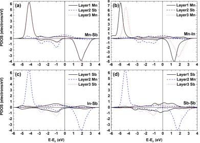
Initially, multilayers of zinc blende MnSb(111)/InSb(111) are investigated. The Mn-to-Sb termination of the interface between a zinc blende half-metallic ferromagnet, MnSb, with 100% spin polarization and InSb both in the (111) direction, is energetically more stable and maintains a high spin polarization of 92.6%. Spin polarization, which is usually reduced or destroyed at the interfaces of half-metallic ferromagnets, is seen to behave differently in the Mn-to-Sb termination of the MnSb(111)/InSb(111) interface structure. And this high spin polarization of 92.6% is injected into the first atomic layer of the InSb(111) slab, before reducing to 40.0% in the fourth atomic layer of the semiconductor slab.
Then the interfaces between niccolite (n)-MnSb(0001) and InP(111) and GaAs(111) were studied in the following chapter. The studies of the n-MnSb(0001)/InP(111) and n -MnSb(0001)/GaAs(111) interfaces show that the Mn-to-P termination of then-MnSb(0001)/ InP(111) and Mn-to-As termination of then-MnSb(0001)/GaAs(111) superlatices have an enhanced spin polarization of 63.9% and 61.1% respectively, which is far higher than the bulkn-MnSb spin polarization of approximately 18%. These interfaces become less energet-ically unfavourable than in the bulkn-MnSb, while the other possible atomic terminations at the interface are more unfavourable.
In the case of the models of Sb(0001)/n-MnSb(0001) interfaces designed. The Sb layer prevents oxidation of the MnSb surface and the Mn-to-Sb termination of these epi-taxial models shows that Sb can grow on MnSb with interesting properties, which agrees with ongoing experimental results. Ionic-covalent bond mix is observed on the Mn-to-Sb termination of the Sb(0001)/n-MnSb(0001) interface, which have a reverse spin polarization of -57.7%.
At the low index interfaces NiO(111)/MgO(111), NiO(001)/MgO(001) and NiO(110)/ MgO(110) a half-metallic ferrimagnetic behaviour is seen on the Ni-to-O termination of the NiO(001)/ MgO(001) interface. Whereas the energetically more favourable Ni-to-O termi-nation of the NiO(111)/ MgO(111) interface structure display a half-metallic like property at its interface.
Chapter 1
Introduction
1.1
Overview
Spintronics is an emerging field of nanotechnology that utilizes the spin state of electrons instead of their fundamental charge to process data in electronic
devices. This involves the detection of electron spins and injecting it from
one material to another. By utilizing the electron spin, it led to faster and
higher density computer hard disk drives. For several decades now metal-based
spintronics has being used in device manufacturing to make spin-valve head
(in hard disk as magnetic sensor), magnetic random access memory (MRAM)
and magnetic tunnel junction magnetoresistive random access memories (MTJ
MRAM) devices with improved storage capacity [1, 2, 3, 4, 5]. These devices
are basically made by sandwiching a non-magnetic layer (metal or insulator)
in between multilayered structure of ferromagnetic materials and uses the gi-ant magnetoresistance (GMR) or tunnel magnetoresistance (TMR) principle.
Combining semiconductors with ferromagnetic materials to form
heterostruc-tures has been considered and shown to exhibit new and interesting feaheterostruc-tures
[6, 7]. This is expected to combine storage, detection, logic and
communi-cation capabilities on a single spintronic device [8]. New device concepts,
such as a spin polarized field effect transistor (Spin FET) have been proposed
[9]. In semiconductor-based spintronics devices, advantages such as increased
data processing speed, improved way of storing information, decreased electric
spin-FET device structure is shown in figure 1.1 with a semiconductor
chan-nel between two ferromagnets. Spin-polarized charge from the source, passes
through the channel to the drain. The spins in FM1 and FM2 layers can
point in the same or opposite direction. The spins can process or not process,
depending on the gate voltage. However, injecting an efficient spin-polarized
current into the semiconductor structure from ferromagnetic contacts is a
com-plex issue and is an important aspect of spintronic devices [12]. Spin injection
is difficult due to the following reasons: conductivity mismatch, interface
reac-tivity, chemical stability of the interface and Schottky barrier height between
the ferromagnetic and semiconducting material [13, 14, 15]. Also, increase in temperature causes a reduction in the spin polarization [6].
Figure 1.1: A spin polarized field effect transistor (Spin-FET) device structure.
To tackle the challenge of inefficient spin injection, either a tunnel
bar-rier (an insulator) or an effective spin source is needed, or a structurally com-patible semiconductor host which will minimise mismatch and allow a smooth
transmission of the spin current generated. Presently, functional materials
such as transition metal pnictides (TMP), ferromagnetic half metals (HM),
antiferromagnets, functional oxides and their interfaces with semiconductors
are explored [16, 17]. Antiferromagnets (e.g. NiO and CuMnAs) can
com-plement or replace ferromagnets as the active components of spintronic
de-vices, which are then called antiferromagnetic spintronic devices [17, 18]. The
net magnetic moment of antiferromagnets is zero and its magnetism is
non-volatile memory devices, such as spin transfer torque (STT) MRAM and
magnetic cloaking. STT MRAM is based on magnetic switching without big
magnetic fields (spin torque effect), which requires only a small bi-directional
current (<150 µA) for its switching operation. While conventional MRAM
is based on field induced magnetic switching and requires two high currents
(>10 mA) for magnetic field generation purposes [19, 20, 21]. A STT MRAM
device has the advantages of low power consumption, high storage density and
easy integration with complementary metal-oxide-semiconductor (CMOS)
cir-cuits. Such a memory device has the added advantage of been robust and
not susceptible to damage from an external magnetic field when made from an antiferromagnetic material due to its net magnetic moment of zero.
Mag-netic cloaking devices can also take advantage of the zero magMag-netic moment
of an antiferromagnet, because, it will be impossible to detect it using regular
magnetic sensors.
An efficient spin generator should have high spin polarization and it is
important to measure the spin polarization of conduction electrons when
inves-tigating the electronic structure of potential materials. The available methods
are spin-resolved photoemission and inverse photoemission, spin-resolved soft
X-ray absorption, and transport measurements in point contacts and tunnel junctions, either with two ferromagnetic electrodes or with one ferromagnetic
and one superconducting electrode1 [22]. The degree of spin polarization can
be defined in several ways and a more general definition can be written as [23]:
Pnvi = (nvi)
↑−(nvi)↓
(nvi)
↑+ (nvi)↓
(1.1)
where n↑(↓) is the density of states (DOS) at the Fermi level and vi↑(↓) is the
velocity of an electron with spin↑ (↓). When i= 0 it is called the DOS spin polarization (see equation 1.2). The velocity of the spin up (↑) electrons could be very slow compared to the spin down (↓) electrons even if their DOS were the same, hence a strong polarization in ballistic transport.
Pn=
n↑−n↓
n↑+n↓ (1.2)
1
A half-metallic binary alloy (e.g. cubic MnSb) [6] has 100% spin
polar-ization at the Fermi level, a high Curie temperature (above 400 K) [14, 6] and
a large magnetic moment per unit cell (4.00 µB) which are important
ingre-dients for a successful fabricated spintronic device to have [24, 25]. However
the structures of these half-metallic binary alloys are metastable. But growing
metastable half metals (HM) on III-V semiconductors could produce films with
stable structures. The half-metallicity in the bulk is affected by increase in
temperature and is usually not preserved at the interface [6]. Here, I will not
be dealing with temperature but we are looking at the interfaces in particular.
A half-metallic binary alloy such as zinc blende MnSb has the needed structural compatibility with conventional zinc blende (ZB) semiconductors
[24, 26]. Combining these two important classes of materials can pave the way
for new devices with improved performance. In this work III-V semiconductors
with exceptional properties and antimony (Sb) has been combined with a
promising TMP MnSb by modelling their heterostructures using first principles
simulation method to find new behaviors at their interface. The HM variant
of nickel oxide (NiO) interfaced with the popularly used insulator material,
magnesium oxide (MgO) was also studied. The TMP MnSb will be introduced
briefly in the next section.
1.2
Structures of the Transition Metal
Pnic-tide MnSb
Transition metal pnictides are made of a transition metal atom (e.g. Mn, Cr
or Ni) and a pnictogen atom (e.g. Sb or As). These materials can crystalize
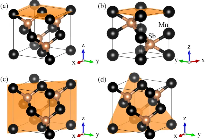
in a range of crystallographic structures (e.g. NiAs-type, zinc blende) and MnSb is a typical example. MnSb usually forms a double hexagonal niccolite
(n) structure with an ABAC stacking order and belongs to the space group
P63/mmc (see figure 1.2 (a)). The stacking arrangement is such that the
transition metal occupies the ’A’ sites, while the pnictogen (Group V) atom
occupies the alternating ’B’ and ’C’ sites. Although, MnSb prefers the
NiAs-type (niccolite) structure, it also exists in two other metastable (cubic [zinc
Table 1.1: Structural properties of the three polymorphs MnSb.
Polymorph Structure Type Space Group Lattice Parameter (˚A)
a c
n-MnSb Niccolite P63/mmc (no. 194) 4.12 5.77 [14]
c-MnSb Zinc blende F¯43m (no. 216) 6.21 6.21 [27] w-MnSb Wurtzite P63mc (no. 186) 4.29 7.00 [6]
polymorphs of MnSb, namely: (a) niccolite (n)-MnSb, (b) cubic (c)-MnSb
and (c) wurtzite (w)-MnSb structures. Their crystallographic information
and lattice parameters are listed in table 1.1. The atoms of a zinc blende unit
cell are said to be tetrahedrally coordinated and those of a niccolite structure
forms a trigonal prismatic geometry.
Figure 1.2: MnSb crystallizes in these Polymorphs: (a) niccolite (n) (b) cubic (c) and (c) wurtzite (w) structure.
1.3
Half-Metals
Half-Metals (HM) are materials that behave like an insulator in one spin
di-rection and a metal in the other. Their DOS plot has 100% spin-polarized
conduction electrons at the Fermi level resulting from a gap, usually in the
spin-down direction [28]. HMs are mainly ferromagnetic (or ferrimagnetic), which include Heusler alloys, oxides, and binary compounds. They are ideal
for spin-dependent electronics because the efficiency of any spin-dependent
device is maximized if the current is 100% spin polarized. Whereas in
conven-tional electronics the charge of the electrons plays the key role of conduction
spin is injected from the HMs to semiconductors. It is imperative to have an
efficient spin injection for the device to be effective.
The three main classes of HMs based on their crystal structure systems
are: Heusler alloys (e.g. NiMnSb), oxides (e.g. CrO2) and zinc blende (e.g.
MnAs, andc-MnSb) type. All HMs have at least one transition metal (TM)
atom (Co, Mn or Fe) in them and their d-states play a major part in the
half-metallicity. When the d-states interacts with other TM atoms d-states,
the p-states of oxygen atoms, pnictides or elements of Group IV, a number of
distinctive properties can be seen. Due to the nature of the atoms involved
and distinct crystal strucuture for each class of HM, their density of states features are dissimilar [11]. Generally the DOS shows s-like states from the
non-TM atoms (oxygens, pnictides and Group IV elements) in the low-energy
region of the valence manifold. In cubic or tetrahedral environment, TM d
-states are divided into triply and doubly degenerate multiplets. For the cubic
case, triply degenerate states are denotedt2g and have lower energy compared
to the doubly states designatedeg. This results as sections of thedxy,dyz, and
dzx states point in the direction of neighboring atoms while parts of the eg
states to second-nearest neighbors. The order of the two states is inverted in
a tetrahedral case. Contingent upon how strong the d-d interaction amongst nearby TM elements is in relation to the d-p interaction (TM and non-TM
elements), the topmost occupied states can either bed ord-p hybridized (see
figure 1.3). The half-metallicity in all three classes of HMs is related to the
d-d and d-p interactions which can be understood in terms of the crystal
field, hybridization, and exchange interaction. In the next paragraph, this
discussion will focus on HMs with the zinc blende structure while interested
readers should look at reference [11, 10, 29] for information on Heusler alloys
and the oxides types.
In the zinc blende structured HMs, the anion for bonding can be a valence IV, V or VI element whose electronegativity is weaker than that of
an O atom. The anion s and p states form sp3 type orbitals and the
five-fold degenerate d-orbitals of the cation (a TM element) split into t2g and
eg-type states as a result of the tetrahedral environment. Energies of the
t2g (dxy, dyz and dzx) states are higher than those of the eg states. The sp3
dzx orbitals point towards each other when close enough and then interact
to form bonding and antibonding states. Given in figure 1.3 are the MnAs
structure and its d-p hybridization. On the left hand side, Mn and As atoms
are represented by black and pink spheres respectively. In the cubic unit cell
Mn atom is positioned at (0.25, 0.25, 0.25)a along the body diagonal and
the primitive cell contains one atom each of Mn and As, where the lattice
parameter a of MnAs is 5.77 ˚A. An overlap of Mn d-orbital and As sp3
orbital is shown on the right-hand side of Fig. 1.3. This overlap generates
bonding and antibonding states. The bonding states, i.e., d-p hybrid states
are covalent in character (charge sharing). Thep-t2g hybrid states bonding has
lower energy than the eg states and more p-character. Figure 1.4 (a) depicts
the schematic diagram of the ordering of orbital energies. Thed-states energy
Figure 1.3: On the left hand side is the MnAs structure with Mn (As) atoms indicated by black (pink) spheres. And on the right hand side is a schematic representaion of the d-p hybridization. Figure from reference [11].
levels of a TM element is given at the left end, while on the right end s
-and p-states energy levels of chalcogenide, pnictide, or carbide can be found.
Crystal field splitting effects can be seen as the centre is approached. The
five-fold degenerate d-states of TM atom split into triply t2g and doubly eg
degenerate states due to the crystal field. sp3-type orbitals are formed by the
non-TM element. Consequential upon thed-p hybridization, are the bonding
(p-t2g) and antibonding (t∗2g) states given at the middle of figure 1.4 (a). A
Figure 1.4: (a) Splitting from the crystal-field under tetrahedral symmetry in the 3d orbitals for a given spin as well as thed-p orbitals hybridization in the ZB structure. Superscripts represent degeneracy. (b) A typical DOS of an HM in the ZB structure. Figure is adapted from reference [11].
only states around the Fermi energy levelEF are visible in the diagram. The
eg (i.e dz2 and dx2−y2) states form the nonbonding states because they point
toward second neighbors instead of the closest neighboring cations. Their energy bands can overlap with or be detached from the d-p bonding states
(p-t2g) and a gap is formed if they are separated. As can be seen in the
spin down (↓) channel, the bonding p-t2g states and nonbondingeg states are
separated by a gap with EF cutting through this gaps. The bonding p-t2g
and nonbonding eg states in the majority-spin (↑) states overlap as shown in
the figure. A substantial anion-p character is in the bonding states whereas
d-p hybrid states with mostly transition-element d character are antibonding
states. In order to allow the unit cell to contain the total number of valence
electrons, the smallest-energy antibonding states in the majority-spin channel are occupied owing to the exchange splitting of majority- and minority-spin
states. Hence half-metallicity emerges as a result of the partial occupation (of
thet∗2g band) in the majority-spin channel. It is worth mentioning that among
the three classes of HMs, hybridization is strongest in the zinc blende (ZB)
HMs because of itsd-p hybrid character nearEF. In the case of Heusler alloys
and oxide HMs, d-states are the leading character near the EF.
For stoichiometric HMs, the last occupied minority-spin band is filled
the magnetization M /µB = (N↑−N↓) gives an integer total moment per cell.
This leads to the Slater-Pauling rule which says the total magnetic moment M
is given by the difference Z−18 (a general expression), where Z is the total number of valence electrons [30, 31, 32].
1.4
Electron Counting Rule for III-V
Semi-conductor Polar Surfaces
In the preceeding section I talked about the behaviour of bulk HM, but as
soon as an interface is made, the bulk symmetries will be broken and the
crystal field picture no longer works because the symmetry environment is
now different. I now need to think carefully about what happens at interfaces
and surfaces to a HM (e.g. Does it maintain the half-metallicity?). A useful
way to check if a semiconductor surface that obeys the electron counting rule is
still a semiconductor (i.e not metallic at the surface) and retains its band gap
at the surface is the electron counting rule. This is analogous to HM, as it is
important that the minority spin gap is maintained at the interface and it does not behave metallic at the surface. Also, the Slater Pauling approach which
says HMs have integer magnetic moment, could be used to check whether this
carries on to the interface [32]. Metals at the surfaces generally relax because
they lack directional bonding while semiconductor surfaces reconstruct because
they have strongly directional bonding. HMs do have covalent bonding and
they might reconstruct on their surface (or interface) [33].
The electron counting rule (ECR) is a method used for predicting the
stability or properties of inorganic compounds. This method can also be
ex-tended from bulk structures to surface and interface models [34, 35, 36]. When a bulk crystal is cleaved, it forms an energetically unfavorable surface as a
re-sult of the dangling bonds (DB) formed during the cleaving process. Figure
1.5 gives an illustration of the zinc blende and niccolite surfaces that are
rele-vant to this thesis. In figure 1.5(a) and (b) the (001) and (0001) surfaces are
respectively given. The cubic system (001) face is a non-polar square
sym-metric surface and forms two dangling bonds per atom. The niccolite (0001)
symmet-rical stacking sequence of the three up and three down bonding, which then
cancels the potential to zero. The Miller index plane (0001) is equivalent to
the (001) plane. Note here that the non semiconductor surface (0001) has
been included because, it is relevant to this thesis. The (110) surface depicted
in figure 1.5(c) is also a non-polar surface since it has equal numbers of anions
and cations. And the (111) surface of a zinc blende crystal shown in figure
1.5(d), which has alternately charged planes is polar. This is a typical Tasker
[image:22.595.141.499.265.510.2]type 3 surface [37].
Figure 1.5: Crystal surfaces showing the: (a) (001) surface of a ZB crystal, (b) (0001) surface of a niccolite structure (e.g. n-MnSb), (c) (110) surface and (d) (111) surface of ZB crystal within the unit cell. The orange shaded area indicates the position of the surface plane.
The more complex surface (111), has an inequivalent number of
dan-gling bonds at its surface. Considering the polar GaAs(111) face with two
possible terminations, A and B. The surface is called (111)A surface, if it is
Ga-terminated and (111)B when it is As-terminated. In the GaAs(111)A
sur-face, each top layer Ga atom has a dangling bond. Removing one of these
energetically unstable. To ensure that it is energetically favourable, it
recon-structs to a (2×2)GaAs(111)A surface with one in four of Ga atoms as surface vacancies (see Fig. 1.6). This vacancy formation allowed for the surface to
transit from metallic-to-semiconducting. From figure 1.6, the removal of one
out of the four surface Ga atoms leaves three dangling bonds in the surface
layer. These can then give their electrons to the three As dangling bonds in
the layer underneath made by the expulsion of the Ga atom. This results
in a filled As dangling bonds and an empty Ga dangling bonds [38, 39, 40].
Reducing the number of dangling bonds, minimises the energy of the surface.
The III-V semiconductors achieve this through the transfer of electrons from the dangling bonds of the Group III element to the dangling bonds of the
Group V element. This electron transfer occurs because of the presence ofsp3
hybridised bonding orbitals in zinc blende structure.
Figure 1.6: (a) Schematic showing the (2×2) GaAs(111)A-Ga vacancy surface reconstruction when viewed from the surface top. The dashed blue (solid black) lines marks the unit cell bounded by Ga (As) atoms. (b) Lateral view of the GaAs(111)A surface slab.
Based on the electron counting rule, the lowest energy surface structure
is obtained when all the available electrons in the surface layer exactly fills
the entire dangling bonds on the Group V element and empty dangling bonds
from Group III element. Note that partially filled dangling bonds may result
to a metallic behavior of the surface. In order to verify if the reconstructed
(2×2) GaAs(111)A surface is ECR compliant, the number of electrons required by the reconstruction is compared with the total number of valence electrons
Table 1.2: Illustration of electron counting for the (2×2) GaAs(111)A recon-struction given in figure 1.6(a).
Group III bonds Group V bonds Group III DB Group V
DB Total e
−
Charge 3/4e− 5/4e− 0e− 2e−
(2×2) 9 9 3 3 24
Total e− from Ga 9
Total e− from As 15
Total Valence 24
surfaces, each of Group III and Group V atoms averagely contributes 3/4e−
and 5/4e− respectively, to make up the total charge of 2e− needed to form a
bond. And charges on Group III dangling bond transfer to Group V dangling
bonds [38]. The total number of dangling bonds and existing dimers on the
surface are added to the non-bulk sigma bonds from the second layer, which
is the layer below the surface. Each of these bonds has 2e− and together
makes up the entire electrons required for the surface reconstruction. This is
then matched with the total number of valence electrons available in the
non-bulk bonding configurations (some valence electrons contributes to the non-bulk bonding). With the (2×2) reconstruction of the GaAs(111)A surface, given in figure 1.6, as a case study, there are 3 Ga atoms on the surface and 4 As
atoms in the layer underneath, but one As atom contributes valence electrons
in the bulk bonding on the third layer (see fig 1.6(a) and (b)). This leaves
3 As atoms available for non-bulk bonding near the surface. Each of the Ga
atoms has a single dangling bond and three III-V sigma bonds and there is no
dimer on this surface, but a Ga vacancy is present. Table 1.2 gives a summary
of the computed values for this structure and it can be seen that the quantity
of electrons required matches the quantity of accessible valence electrons thus the structure obeys the ECR. Semiconductors such as: Si, Ge, InP, InSb and
others also reconstruct on their surfaces to form stable surface structures.
Zhang et al, proposed an extension of the ECR to account for
metal-induced surface reconstruction of compound semiconductors [41]. These
ad-justed principles are known as the generalized electron counting rules (GECR)
and they depend on three extra requirements. The first, is concerned with the
adatoms (Mn, Cr or Fe) prefer to occupy interstitial sites near the III-V
sur-faces andsp (ors) metals like Ag, Al, as well as Au prefer to occupy the
substi-tutional sites. The second GECR suggests that a metal adatom will serve as a
donor or an acceptor depending on its Pauling electronegativity value relative
to those of the constituent elements of the semiconductor. The third GECR
states that surface reconstructions which minimize (maximize) the total
num-ber of valence electrons on the metal atoms (nR) for metal donors (acceptors)
are the lowest in energy. nR can be given as:
nR=vMnM + 3nIII + 5nV −2nbonds (1.3)
where vM represent the number of valence electrons on a metal adatom and
nbonds is the total number of bonds (both sigma bonds and occupied DBs)
formed around the surface. On the reconstructed surface nM, nIII and nV
are respectively the number of metal, Group III and Group V atoms. The
net charge transfer from the metal adatoms to the substrates is given by
vMnM − nR. Equation 1.3 reverts to the classic ECR for low-energy
sur-face reconstructions, if there is no metal adatom (i.e nM = 0 and nR ≡ 0).
Hence, with the adsorption of metal adatoms, the preferred structure is one
that yields the lowest possible value ofnR.
1.5
Organization of the Thesis
In this thesis, we use density functional theory (DFT) to investigate the
inter-face properties between the transition metal pnictide, MnSb and some III-V
semiconductors. Also, the characteristics of half-metallic NiO and insulating
MgO interfaces are investigated. This study aims to determine the structural,
electronic and magnetic properties at the interfaces of these epitaxial growth
models. Chapter 2 reviews the theoretical background and underlying princi-ples for a DFT approach, and software packages used to successfully implement
a simulation are briefly introduced. The half-metallicity of cubic (c)-MnSb
and its interfaces with the high mobility semiconductor InSb is described in
Chapter 3. Chapter 4 is devoted to the study of niccolite (n)-MnSb/InP and
inter-facial systems are compared. Chapter 5 discusses the interaction of n-MnSb
with the semi-metal Sb. Chapter 6 focuses on NiO/MgO interfaces in different
crystal directions. Finally, a summary and the key conclusions of this study
Chapter 2
Theoretical Background
2.1
Density Functional Theory
DFT is an effective method of approximately solving the many body Schr¨odinger equation for electrons, which describes the properties of materials at the
atomic, molecular and condensed scales [42, 43]. It is widely used by
re-searchers across various disciplines because of its low computational cost
com-pared to full quantum mechanical calculations [43, 44, 45]. The foremost
no-tion of DFT is to make use of the density of the electronn(r) as the argument
to functionals, which determine the properties of a many body system [44, 46].
To study the various properties of a material I approach it based on the
true, fundamental Hamiltonian of the many-electron system. This approach
is called ab-initio or first principles [42]. A simple way to start is to write the
time-independent, non-relativistic case, of the many-body Schr¨odinger equa-tion for the material as:
HΨ = EλΨλ (2.1)
where,H is the Hamiltonian operator, Eλ is an energy eigenvalue and Ψλ an
eigenstate of the Hamiltonian. If the system were to be a particle in a box or
a harmonic oscillator case which has a simple Hamiltonian, the Schr¨odinger
equation can be solved exactly.But the physical system I have to deal with has
many electrons interacting with many nuclei in a complex way [43]. So, the
" −~ 2 2m N X i=1 ∇2i +
N X
i=1
V(ri) + N X
i=1 X
j<i
U(rirj) #
Ψλ =EλΨλ (2.2)
where m is the mass of each electron, the terms in bracket are: the kinetic
energy operator ˆT of the individual electron, the potential energy ˆV between each electron and the collection of atomic nuclei, and the electron-electron
interaction energy ˆU respectively. I can rewrite equation 2.2 based on ˆT, ˆV
and ˆU for the ground state wave function and ground state energy.
h
ˆ
T + ˆV + ˆUi|Ψoi=E|Ψoi (2.3)
The wave function Ψ for this many-body problem ofN electrons has 3N spatial
coordinates ri, and N spin coordinates σi, hence, Ψ = Ψ(r1σ1, . . . ,rNσN). In
equation 2.2 I have ignored the motion of the atomic nuclei (Born-Oppenheimer
approximation) and choose to look at the ground state wave function Ψo
with ground state energy E. Various methods have been developed to ap-proximately solve the many-body Schr¨odinger equation given in equation 2.2.
The Hartree-Fock (HF) approximation is the oldest and simplest one. There
are others such as the free electron model (FEM) and Thomas-Fermi model
[43, 42].
Now let us look at the DFT method of approximately solving the
many-body system. Foundation is given by Hohenberg and Kohn (HK) theorems
and the Kohn-Sham (KS) equations [46, 47]. Consider a non-magnetic system
with a non-degenerate ground state described by the non-relativistic
time-independent Schr¨odinger equation 2.2 or 2.3. The first HK theorem says: The ground-state energy E can be expressed as a unique functional of the
electron density E[n(r)]. This means the information about the ground state
properties is contained in the ground state electron density. The second HK
theorem goes on to tell us about a feature of this functional: the true ground
state electron density agreeing with the complete solution of the Schr¨odinger
equation minimizes the total energy functional E[n(r)]. In order words, one
should vary the likely densities and choose the one that gives the minimum
(i.e. its expectation value) given by HK theorem [46],
E[n(r)] =hΨo|[ ˆT + ˆV + ˆU]|Ψoi (2.4)
E[n(r)] =T[n(r)] +U[n(r)] +
Z
d3rVext(r)n(r) (2.5)
The kinetic energy of the electronsT and Coulomb potential from the electron-electron interaction U are independent of the external potential Vext. I can
further rewrite equation 2.5 as:
E[n(r)] =Ts[n(r)] +
1 2
Z
d3rd3r0n(r)n(r 0
)
|r−r0| +Exc[n(r)] +
Z
d3rVext(r)n(r)
(2.6)
Ts is the kinetic energy of a putative non-interacting particle system with a
ground state density n(r), and the second term is the classical Coulomb
in-teraction. Exc[n(r)] is the exchange and correlation energy functional which
has all remaining many-particle effects in it: the many-particle input to the
kinetic energy and Pauli exclusion principle effects [44]. At this stage it is still impossible to solve the many-body Schr¨odinger equation because the
func-tionals Ts[n(r)] and Exc[n(r)] are unknown, though numerous fairly accurate
functionals have been suggested for the later.
To find the minimum energy solutions of the total energy functional,
Kohn and Sham (KS) came up with a scheme that transforms the
many-particle problem to a single-many-particle one and gives a set of equations similar to
Schr¨odinger’s [44, 47]. It is called the Kohn-Sham (KS) equation and is given
as:
−1
2∇
2+V ext+
Z
d3r0 n(r) |r−r0|+
δExc[n(r)] δn(r)
ψi(r) =iψi(r) (2.7)
where, from the left-hand side, the second term is the external potential Vext
due to the interaction between an electron and the collection of atomic nuclei.
The third term is the Hartree potential VH which is the Coulomb repulsion
between the electron under consideration and the total electron density. The
next term is the functional derivative ofExc with respect to n(r) . This is the
energy Exc. Solving equation 2.7 self-consistently we obtain the electron
den-sity at ground state:
n(r) =
N X
i=1
|ψi(r)| 2
(2.8)
Knowing the solution{i, ψi(r)}to equation 2.7, I can now write the unknown
functionalTs[n(r)] as
Ts[n(r)] = N X
i=1 i−
Z
d3r{Vext(r) +VH(r) +Vxc(r)}n(r) (2.9)
The KS equations are solved in an iterative way until a self-consistent solution is obtained. The Kohn-Sham approach has proven to be reliable for calculating
ground state properties for many-body systems with a precision that matches
experimental data [44, 45]. Now I can write the total energy expression as
E[n(r)] =
N X i=1 i− 1 2 Z
d3rd3r0n(r)n(r 0
)
|r−r0| −
Z
d3rVxc[n(r)]n(r) +Exc[n(r)]
(2.10)
There is still one more complication which is that the true exchange
correlation functional is not known. This term is approximated in some way to
get an approximate energy and this makes the variational principle somewhat
suspect. However, variational principle is still used and the density obtained is
taken as the ground state density. The variational principle says: the computed
energy from any trial wave functions will be higher than the true ground state
energy, but equals it if the trial wave function is identical to the true ground state wave function. Several approximations for Exc[n(r)] are in use today
and the popular ones are: local density approximation (LDA), generalized
gradient approximation (GGA) and hybrid functionals. LDA uses only the
local electron density to replace the exact exchange-correlation functional by
ExcLDA[n(r)] =
Z
d3rn(r)xc(n(r)) (2.11)
where xc(n(r)) is the exchange and correlation energy per particle of a
ho-mogeneous electron gas with density n(r). Though it works very well but it
(about 0.5 ˚A less) and slightly large bulk moduli (say 5 more) from the actual
values for a given material [44]. It can give incorrect order of phase stability
and errors in the energetics of magnetic materials, hence GGA is often used in
this work [48]. Note that the HK and KS treatment above can also be applied
to magnetic systems, in which case the spin component (e.g, n = n↑n↓) is
included. Rewriting equation 2.11 to represent the local spin density (LSD)
approximation for an electron gas of uniform spin densities n↑(r), n↓(r) gives:
ExcLDA[n↑(r), n↓(r)] =
Z
d3rn(r)xc(n↑(r), n↓(r)) (2.12)
GGA uses the electron density and its gradient which gives rise to a
huge number of different GGA functionals, because it needs a mix of n(r) and ∇n(r) to be decided ad hoc. The two most common are Perdew-Wang functional (PW91) and Perdew-Burke-Ernzerhof functional (PBE), which in
section 2.2 I have provided further details on. Although GGA is better than
LDA in some ways, it still does not deal with the issues of strongly correlated
systems, for instance transition metal oxide and heavy fermion systems. To
correct this, schemes such as LDA+U or GGA+U are used, which have an
orbital-dependent interaction term called the Hubbard U parameter [43, 44].
Hybrid functionals are made from an orbital-dependent Hartree-Fock part and
an explicit density functional. They are usually preferred by quantum chemists over LDA and GGA for atomic and molecular calculations [44].
2.2
Generalized Gradient Approximation
The generalized gradient approximation (GGA) is an extension of LDA where
information about the electron density n(r) as well as its gradient ∇n(r) is used to provide an account of the non-homogeneity of the true electron density.
These functionals are at the centre stage of modern DFT and can be expressed generally as:
ExcGGA[n↑, n↓] =
Z
d3rf(n↑, n↓,∇n↑,∇n↓) (2.13)
but a rational choice can be made by considering the derivations and
pre-scribed properties of a given GGA fuctional and its suitability for the material
system under study. GGA typically provides a more accurate description of
atoms, molecules and solids than the local spin density (LSD) approximation.
It typically minimizes the error due to bond dissociation energy as well as
improves the total energies, atomization energies, transition-state energy
bar-riers and structural energy differences [49, 50, 51, 52]. ExcGGA[n↑, n↓] is usually
separated into its exchange and correlation terms, i.e.
ExcGGA =ExGGA+EcGGA (2.14)
A prominent representation to simplify this GGA was first given by
Perdew and Wang in 1986 [53]. In order for this functional to be used routinely
in self-consistent calculations for atoms, molecules and solids, the exchange
energy as a functional of the density was approximated as:
ExGGA[n] =Ax Z
d3rn4/3Fx(s) (2.15)
where,
Ax =−
3 4(3/π)
1/3
(2.16)
s =∇n/(2kFn) (2.17)
kF = (3π2n)1/3 (2.18)
and
Fx(s) = (1 + 1.296s2+ 14s4+ 0.2s6)1/15 (2.19)
The function Fx(s) is an analytical fit. The functional form of equation 2.15
scales properly as an exchange energy [54]:
Ex[nγ] =γEn[n] (2.20)
where nγ(r) = γ3n(γr) represent the scaled density. A corresponding
spin-scaling exchange energy for a spin density functional can be constructed as:
Ex[n↑, n↓] =
1
2Ex[2n↑] + 1
The functional derivative of exchange energyEGGA
x [n] is the exchange potential
needed for a self-consistent calculation
δEx
δn(r) =Axn
1/3
4
3F −ts
−1dF ds −
u−4
3s 3 d ds
s−1dF ds
(2.22)
where,
t= (2kF)−2n−1∇2n (2.23)
and
u= (2kF)−3n−2× ∇n· ∇ |∇n| (2.24)
As |r| → ∞, the functional derivative for this GGA tends to zero. For a spin-density functional, one constructs the exchange potential from:
δEx[n↑, n↓] δnσ(r)
= δEx[n]
δn(r) |n(r)=2nσ(r) (2.25)
This real-space cutoff construction of GGA functional was later extended from
exchange to correlation, which led to Perdew-Wang 1991 (PW91) GGA forExc
[55, 56]. Then in 1996, Perdew, Burke and Ernzerhof (PBE) came up with a
much simpler way of constructing PW91 functional with some improvements
[57]. Practically, PBE is equivalent to PW91 and they produce essentially the
same results, however PBE describes the linear response of uniform electron gas more accurately. PBE achieves this accuracy by allowing the electron gas
to behave correctly under uniform scaling and have a smoother potential.
To construct the PBE functional, it is normal and important to impose
the real-space cutoff condition used for the construction of PW91 [53, 58]. The
PBE derivation will be summarized here, an interested reader can look at the
references [57, 56] for a detailed discussion. A GGA(PBE) construction for
correlation energy begins in the form
EcGGA[n↑, n↓] =
Z
d3rn[c(rs, ζ) +H(rs, ζ, t)] (2.26)
has one electron and is defined in the equation below:
n = 3 4πr3
s
= k
3 F
3π2 (2.27)
The relative spin polarizationζ is given as:
ζ = n↑−n↓
n (2.28)
and t is the reduced density gradient, which is a dimensionless quantity.
t= |∇n| 2φksn
=π 4
1/29π
4
1/6
s
φrs1/2
(2.29)
Hereφ is a spin-scaling factor [59],
φ(ζ) = [(1 +ζ)
2/3+ (1−ζ)2/3]
2 (2.30)
and
ks = r
4kF πa0
(2.31)
is Thomas-Fermi screening wave number (a0 = ~2/(me2)). The density
pa-rameters rs and ζ are local, while the density n is equivalent to n↑ +n↓ in
cases that involves spin-densities. H(rs, ζ, t) is the density gradient
contribu-tion. Under uniform density scaling of nγ(r) = γ3n(γr) to the high-density
limit (γ → ∞),EGGA
c [n↑, n↓] from equation 2.26 tends to a negative constant:
EcGGA[nγ]→ − e2 a0
Z
d3rnγφ3ln
1 + 1
χs2/φ2+ (χs2/φ2)2
(2.32)
where the dimensionless density gradient s is defined by equation 2.17 and
χ = (β/γ)c2exp(−ω/γ) ∼= 0.72161(β ∼= 0.066725, γ ∼= 0.031091, c ∼= 1.2277
and ω ∼= 0.046644). For a two-electron ion of nuclear charge Z → ∞, the correlation energy is exactly -0.0467.
To construct the PBE GGA for the exchange energy, apply the
2.33 forζ = 0 everywhere. The uniform gas exchange energyx =−3e2kF/4π.
ExGGA =
Z
d3rnx(n)Fx(s) (2.33)
In order to recover the useful LSD description of the linear response of the
uni-form gas, the gradient coefficient for exchange must cancel that for correlation
(ass→0). This leads to,
Fx(s)→1 +µs2 (2.34)
whereµ=β(π2/3)∼= 0.21951. Also, we want the Lieb-Oxford bound
Ex[n↑, n↓]≥Exc[n↑, n↓]≥ −1.679e2 Z
d3rn4/3 (2.35)
to be satisfied [56]. This can be achieved with the simple form
Fx(s) = 1 +k−
k
(1 +µs2/k) (2.36)
which satisfies equation 2.34 as well. Here k is a constant less than or equal
to 0.804.
A good way to portray the nonlocality of the PBE GGA exchange and
correlation, is to write
ExcGGA[n↑, n↓] =
Z
d3rnx(n)Fxc(rs, ζ, s) (2.37)
by defining an enhancement factor Fxc(rs, ζ, s) over spin-unpolarized (ζ = 0)
local exchange [49]. The effects of correlation (rs-dependence), spin
polariza-tion (ζ), and nonlocality (s-dependence) can be shown by the enhancement
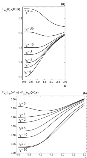
factor. Figure 2.1(a) displays thes-dependence of the enhancement factor for a
spin-unpolarized (ζ = 0) system. While, Figure 2.1(b) shows the enhancement
factor for the difference between the fully spin-polarized (ζ = 1) and
unpolar-ized (ζ = 0) Fxc(rs, ζ, s) [56]. The high-density-limit (rs → 0) is dominated
by the exchange-only enhancement factor. By definitionFx(ζ = 0, s= 0) = 1
asrs →0, see figure 2.1(a). At fixedrs (decrease rs), as the reduced gradient s increases, exchange is strongly turned on, whereas correlation is turned off.
in the low-density-limit (rs → ∞), as a result nonlocality is dominated by
correlation. Note that for a fully spin-polarized system (rs → ∞, ζ = 1),
non-locality is approximately cancelled in the low-density-limit and the
exchange-correlation hole becomes local. In the range 0 ≤ s ≤ 1, the exchange and correlation nonlocalities are opposite, and tend to cancel for valence-electron
densities (1≤rs ≤10).
2.3
Hubbard U and DFT+U
The local density approximation (LDA) and generalized gradient
approxima-tion (GGA) have been successful in describing a nearly uniform electron
den-sity, but they fail in the non-uniform bound of localized electronic states with
strongly correlated electrons. In other words, on-site Hubbard-like (Coulomb)
interactions are not correctly treated in the LDA/GGA formalism, while
screen-ing correlation effects can be well described by these functionals [60, 44].
DFT+U is based on a correction to the standard functional, by providing
an improved description of the electronic states of strongly correlated
sys-tems (typically, localized d or f orbitals). This is done by adding an on-site Hubbard-like (U) interaction to the approximate DFT total energy of a system
[60, 61, 62]:
ELDA+U[n(r)] =ELDA+U[n(r)] +EHub[
nIσm ]−EDC[
nIσ ] (2.38)
whereELDA is the total energy functional being corrected,EHub encompasses
the Hubbard Hamiltonian for correlated states, andEDCis the double-counting
(DC) term. The DC functional is not uniquely defined and different forms
have been used. However, in the unitary-transformation-invariant formulation
of LDA+U, more general expressions ofEHub and EDC were given:
EHub[
nImm0 ] =
1 2
X
{m},σ,I
hm, m00|Vee|m0, m000inIσmm0nIm−00σm000
Figure 2.1: The enhancement factorFxcof equation 2.37 for the Perdew, Burke
EDC
nImm0 =
X
I
UI
2 n
I(nI−1)− JI
2
nI↑(nI↑−1) +nI↓(nI↓−1)
(2.40)
HerenIσ
m are the occupation numbers of localized orbitals, I is the atomic site
index, m is state index and σ is the spin. nIσ
mm0 is given as:
nIσmm0 =
X
k,v
fkvσ ψkvσ |φIm0 φIm|ψkvσ
(2.41)
where the coefficient fkvσ denote the occupations of KS states. The first term on the right hand side of equation 2.39 inside the bra-ket notation can be
written as:
hm, m00|Vee|m0, m000i= 2l X
k=0
ak(m, m0, m00, m000)Fk (2.42)
Here l is the angular moment of the localized (d or f) electrons and ak the
angular factors is given below
ak(m, m0, m00, m000) =
4π
2k+ 1
k X
q=−k
hlm|Ykq|lm0i
lm00|Ykq∗|lm000 (2.43)
The parameters Fk (F0, F2, and F4 for d electrons, while f states require
F6 to compute the matrix elements Vee) are the radial Slater integrals. The
screened on-site Coulomb (U) and exchange (J) interaction can be expressed as:
U = 1
(2l+ 1)2 X
m,m0
hm, m0|Vee|m, m0i=F0 (2.44)
J = 1
2l(2l+ 1)
X
m6=m0,m0
hm, m0|Vee|m0, mi=
F2+F4
14 (2.45)
Once U and J have been calculated, the Fk parameters (as well as Vee) are
extracted using the above equations by presuming atomic values for F2/F4
and F6/F4 ratios (e.g., F2/F4 = 0.625).
A simplified expression of EHub and EDC for the rotationally invariant
order integralsF0 and setting F2 =F4 =J = 0 is as follows:
EU
nIσmm0 =EHub
nImm0 −EDC
nI =X I UI 2 "
(nI)2−X σ
T r(nIσ)2
# −X I U0 2 n I
(nI−1)
= U 2
X
Iσ
T r[nIσ(1−nIσ)] (2.46)
Diagonalizing the occupation matrices based on the localized orbitals
repre-sentation
nIσvIσi =λIσi vIσi (2.47)
with the constraints 0≤λIσ
i ≤1, where λIσi and vIσi are respectively
eigenval-ues and eigenvectors. The Hubbard correction for the energy becomes:
EU
nIσmm0 = U 2 X Iσ X i
λIσi (1−λIσi ) (2.48)
with this, the corrective functional can be derived from just one interaction
parameter (U). It is normal to express the Coulomb interaction U in terms
of an effective value that includes the Hunds rule coupling J :Uef f =U −J.
It provides a more accurate account of on-site electron-electron interaction,
capturing the localization of electrons. The Hubbard correction occasionally gives close to experimental band gap value in the band structure for some
materials (e.g. NiO and MnO) due to crystal field splittings or Hunds rule
[63, 64]. The U should not be used as an adjustable parameter to mimic
experimental band gaps.
2.4
Plane waves and Pseudopotentials
There are various computational methods employed to solve the Kohn-Sham (KS) equations of 2.7, like Hartree-Fock (HF), Korringa-Kohn-Rostoker (KKR),
energy for the finished calculation is written as
E =− occ X
i Z
d3rϕ∗i(r)∇
2
2 ϕi(r) +
Z
d3rvext(r)n(r)
+1 2
Z
d3r
Z
d3r0n(r)n(r 0)
|r−r0| +Exc (2.49)
where on the right on side, the first term is the non-interacting kinetic
en-ergy, the second term is the external potential, next is the Hartree term and finally, the exchange-correlation energies. To make equation 2.49 suitable for
implementation in most DFT codes, it can be simplified further to yield:
E =
occ X
i εi−
Z
d3r
1
2vH(r) +vxc(r)
n(r) +Exc (2.50)
and the electronic density is defined as:
n(r) =
occ X
i
|ϕi(r)|2 (2.51)
In order to account for interactions between ions (Enn), a repulsive Coulomb
term should be added to the total energy in a geometry optimization
calcula-tion
Enn = X
α,β
ZαZβ |Rα−Rβ|
(2.52)
2.4.1
Plane-waves basis sets
To expand the Kohn-Sham electronic wave functions, a plane-wave basis set is
essential, since it makes better use of the periodicity of crystals. The number
of plane-waves basis set required is very large and it can be truncated to a finite
number of plane-wave functions, below a particular cutoff energy [56, 66].
Based on Blochs theorem for a periodic solid, the electronic wave-functions can be written as
ϕk,n(r) =eik·r X
G
where k is the wave vector, the band index is n, and the reciprocal lattice
vectors are represented by G. The plane-wave representation of Kohn-Sham
equations assume the following form
X
G0
1
2|k+G|
2δ
G,G0 +vion(G−G0) +vH(G−G0) +vxc(G−G0)
ck,n(G0)
=εk,nck,n(G) (2.54)
where the various potentials have been given in terms of their Fourier
trans-forms. Equation 2.54 can be solved by diagonalizing the Hamiltonian matrix,
represented by the terms in the brackets. To limit the size of the matrix (or
G) an energy cutoff is set up
|k+G|2
2 ≤Ecut (2.55)
But a very large G (many plane waves) is needed to describe accurately the
wave functions of material systems, which is a severe problem. This is because
the core electrons are tightly bound to the nuclei in solids or molecules and
the wave functions of the valence electrons change rapidly in the core region.
With the application of the pseudopotential approximation, this challenge can
be overcome.
2.4.2
Pseudopotentials
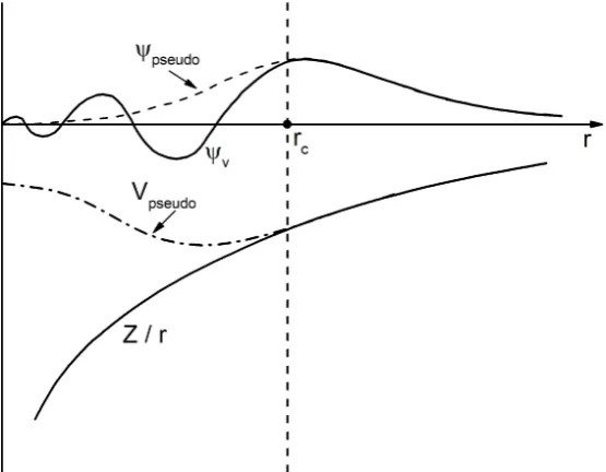
A vital component of many DFT calculations is the pseudopotentials, which
uses the fact that most physical properties of solids are mainly due to the
valence electrons. The pseudopotential method treats core electrons as frozen
entities and approximates the potential felt by the valence electrons to a weaker pseudopotential that can reproduce smooth wave functions (pseudo wave
func-tions) of the valence electrons instead of the true valence wave functions.
Fig-ure 2.2 shows an ionic potential, valence wave function then an equivalent
pseudopotential and pseudo wave function. The wave function of a valence
electron undergoes rapid oscillation in the core electron region owing to the
strong ionic potential in this region. As a result of these oscillations the
func-tions. The pseudopotential is constructed in such a way that the pseudo wave
functions do not have radial nodes in the core region. Outside the core region
(beyond the distancerc = 1.3 au), the all electron and pseudoelectron
poten-tials are similar (see fig. 2.2) as well as their wave functions [66]. Generally,
[image:42.595.182.460.207.423.2]pseudopotentials are mostly expressed as:
Figure 2.2: Comparison of all electron (solid lines) and pseudoelectron (dashed lines) potentials and the wave functions (ψ) they represents. rc depicts the
radius at which all electron and pseudoelectron values meet. The figure is a remake of figure 5 in Ref. [66].
VN L= X
lm
|lmiVlhlm| (2.56)
where |lmi are the spherical harmonics and Vl is the pseudopotential for
an-gular momentum l. A pseudopotential is said to be local, when it uses the
same potential for all angular momentum components. Local pseudopotentials
have a very high computational efficiency compare to nonlocal ones, but just
a handful of elements can be described correctly with local pseudopotentials.
In pseudopotential applications, the amount of hardness of a
pseudopo-tential is important. When a pseudopopseudopo-tential requires a small (large) number
pseu-dopotential. Norm-conserving pseudopotentials for transition metals and first
row elements in the early days of the method were extremely hard due to
their high cutoff energy, hence there was the need to find a way to improve
convergence properties of this potentials1.
An approach which involves relaxing the norm-conservation condition
in order to generate much softer pseudopotentials was suggested by Vanderbilt
[67]. This is the ultrasoft pseudopotential scheme, where calculations with the
lowest possible cutoff energy for the plane-wave basis set is allowed. Ultrasoft
pseudopotentials have much better energy transferability and accuracy, and it
usually treats shallow core states as well a valence states. In the Vanderbilt ultrasoft pseudopotential (usp) scheme, which reduces the number of plane
waves and energy cutoff required to describe electronic wave functions [67, 68],
the total energy of the valence electrons Nv, described by the wave functions
φi, is given by
Etot[{φi},{RI}] =
X
i
φi| − ∇2+VN L|φi
+1 2
Z Z
drdr0n(r), n(r
0)
|r−r0|
+Exc[n] + Z
drVlocion(r)n(r) +U({RI}) (2.57)
whereU(RI) is the ion-ion interaction energy, Vlocion(r) = P
IVlocion(|r−RI|) is the local pseudopotential and the nonlocal pseudopotential is given by
VN L = X
nm,I
Dnm(0)|βnIihβmI| (2.58)
where the functions βI
n and coefficients D (0)
nm characterize the pseudopotential
and differ for different atomic species. The indicesn and m run over the total
number of angular momentum eigenfunctions βn, and I represents an atomic
site. The electron density is given by
n(r) =X
i "
|φi(r)|2+ X
nm,I
QInm(r)hφi|βnIihβ I m|φii
#
(2.59)
1http://www.tcm.phy.cam.ac.uk/castep/documentation/WebHelp/content/pdfs/
where the augmentation functions QI
nm(r) are strictly localized in the core
regions. In equation (2.59) the electron density has been separated into a
soft delocalized contribution given by the squared moduli of the wave
func-tions, and a hard localized part at the cores. The ultrasoft pseudopotential is
completely determined byVion loc (r), D
(0)
nm, QInm(r), and βn(r).
The relaxation of the norm-conserving restraint is achieved by
intro-ducing a generalized orthonomality condition
hφi|S(RI)|φji=δij (2.60)
Here the Hermitian overlap operatorS is given by
S = 1 +X
nm,I
qnm|βnIihβ I
m| (2.61)
and qnm is equivalent to the integral of Qnm(r). S is dependent on the ionic
positions through the term |βI
ni, βnI(r) = βn(r−RI). Based on the ultrasoft
pseudopotential scheme the Kohn-Sham equations can be expressed as:
H|φii=εiS|φii (2.62)
whereεi represents Lagrange multipliers, and
H =−∇2+V ef f +
X
nm,I
DnmI |βnIihβmI| (2.63)
The screened effective potentialVef f, is given as
Vef f(r) = Vlocion(r) + Z
dr0 n(r
0)
|r−r0| +µxc(r) (2.64)
where µxc(r) = δExc[n]/δn(r). All the terms arising from the augmented
portion of the electron density are grouped with the nonlocal part of the
pseu-dopotential (eq. 2.58) by defining new coefficients
DInm=Dnm(0) +
Z