Service Procedures for:
Q068, Type 300 12V Autopilot Course Computer (Z166 Core Pack)
Q069, Type 300 24V Autopilot Course Computer (Z167 Core Pack)
Q067, Type 100 12V Autopilot Course Computer (Z168 Core Pack)
CE MARKING OF EQUIPMENT/REPLACEMENT PARTS
WARNING
If the Autohelm equipment under repair, test, calibration, installation or setting to work carries the European CE mark, only parts and components supplied or approved for such use by Autohelm should be used in order to maintain compliance with the relevant CE requirements.
Incorporation, use or attachment, by any means, of parts or components not supplied for or not approved for such use by Autohelm or, if supplied or approved for use by Autohelm, not properly fitted in accordance with instructions published, provided or recommended by Autohelm, may cause the equipment to malfunction and, in particular, to become unsafe or to no longer meet the relevant CE requirements. In these circum-stances, Raytheon Marine Europe Ltd excludes liability to the fullest extent permissible in law for any loss or damage including any liability for its contribution to such loss or damage by its negligent acts or omissions .
Contents
1. Description ... 5 1.1 General ... 5 1.2 Variants ... 5 2. Operation ... 5 3. Disassembly ... 6 4. Assembly ... 6 5. Functional Test ... 95.1 Pre - checked Equipment Required ... 9
5.2 Functional Test Procedure ... 9
5.3 Functional Test Flowchart ... 11
6. Product History ... 13 6.1 Q067, Type 100 ... 13 6.2 Q068, Type 300 (12V) ... 13 6.3 Q069, Type 300 (24V) ... 14 7. Software History ... 15 7.1 Q067, Type 100 ... 15 7.2 Q068, Type 300 (12V) ... 15 7.3 Q069, Type 300 (24V) ... 15 8. Spares Numbers ... 17 8.1 Q067, Type 100 ... 17 8.2 Q068, Type 300 (12V) ... 17 8.3 Q069, Type 300 (24V) ... 18 9. Circuit Description ... 19 9.1 Power Supplies ... 19
Type 100 and Type 300 (12V)... 19
Type 300 (Q068) ... 21
9.3 Input/Output Signals ... 26
10. PCB Layouts and Component Lists ... 28
10.1 12V Computers, Type 100 (Q067) and Type 300 (Q068) ... 28 10.2 24V Computer, Type 300 (Q069) ... 31 10.3 PCB Components, Type 100 12V (Q067) and Type 300 12V (Q068) ... 32 10.4 PCB Components, Type 300 24V (Q069) ... 35
Illustrations
Figure 1 Exploded View ... 7 Figure 2 Location Comb Assembly Detail ... 8 Figure 3 Connections to Terminals ... 10 Figure 4 Block Diagram of 12V Power Circuits, Type 100 (Q067) and Type 300 (24V) ... 22 Figure 5 Generation of RLY - 0V ... 21 Figure 6 Block Diagram of 24v Power Circuits Type 300 (Q069) ... 22 Figure 7 Logic Circuits Block Diagram, All Variants ... 25 Figure 8 Terminal Block Numbering ... 27 Figure 9 PCB Layout Type 100 (Q067) and Type 300 12V (Q068) 28 Figure 10 Circuit Diagram 12V Computers, Type 100 (Q067) and Type 300 (Q068) ... 29 Figure 11 Circuit Diagram, 24V Computer Type 300 (Q069) ... 30 Figure 12 PCB Layout, Type 300 24V (Q069) ... 31
1. Description
This section of the Maintenance Manual covers all three variants of the Course Computer:
Q068, Type 300 12V Autopilot Course Computer (Z166 Core Pack) Q069, Type 300 24V Autopilot Course Computer (Z167 Core Pack) Q067, Type 100 12V Autopilot Course Computer (Z168 Core Pack)
1.1 General
The Type 100/300 Course Computer is SeaTalk compatible and consists of a case containing a PCB which carries a microcontroller, drive unit, power amplifier, protection relays and a connector block for all inputs and outputs.
Type 100 is used with Type 1 and Type CR 12V drives. Type 300 is used with Type 2 and Type 3 12V or 24V drives.
1.2 Variants
Functions of all three variants are identical. The difference between Type 300 24V and Type 300 12V is the input voltage and motor output voltage. Between 12V variations, Type 100 and Type 300, the difference is the power handling capabilities of the motor output.
All other inputs and outputs (SeaTalk, compass etc.) produce or need the same signal levels whatever the variant.
Mechanically, all three variants are identical in that the computer consists of a case with top and bottom parts containing a PCB.
2. Operation
3. Disassembly
Refer to Figure 1, Exploded View. 1. Remove the terminal cover (1)
2. Unscrew and remove the four M3 screws (12) on the lower case (11). Remove the lower case
3. To remove the PCB (8), unscrew and remove the five M2 screws (9). Unscrew by two or three turns the location comb screws (5). (Note that computers from serial number 0360001 use machine screws and require a 2.5mm hexagon key). Access to these screws is gained through two holes in the PCB, one of which is shown in Figure 2, behind and to the left (as viewed) of the line of FETs (13). Do not remove the screws at this stage. Lift the PCB out of the upper case (2)
4. Remove the location comb (4) by unscrewing and removing the two screws (5)
5. If the insulation strip (3) is damaged, out of position or a new location comb is to be fitted (see Assembly Instruction 3), carefully peel off the old strip and clean any remaining adhesive and heat transfer com-pound off the case
6. The insulating strip (10) fits over the legs of the connectors and can be removed if necessary.
4. Assembly
Refer to Figure 1, Exploded View and Figure 2, Location Comb Assembly Detail.
1. Apply heat sink compound (14) to the area of the case where the insulation strip (3) fits. Apply double sided sticky tape to the case and attach the insulation strip as shown in Figure 2 detail 1. Bend the strip over the edge and apply a second layer of heat transfer compound (Figure 2 detail 2)
2. Fit the location comb (4) into the upper case (2) with the two M2 screws (5). Do not tighten the screws at this stage. (Note: Check that the location comb has the new shape as shown in Figure 2. If not, use Autohelm Course Computer Modification Kit Q098 to replace the old shape comb with a new shape comb)
3. To replace the PCB (8) in the upper case (2), hold the lower case so that the location comb falls away from the insulation strip (3). Ensure that the lip of the location comb does not come out of the flange in the case.
4. Position the PCB next to the upper case (2) and bring the two together so that the FETs (13) are between the location comb (4) and the insula-tion strip (3) (Figure 2 detail 3) . Ensure that the lip of the locainsula-tion comb
1. Terminal cover 2. Top case 3. Insulation strip 4. Location comb
5. Location comb screw (2 off)
7. Fuse 8. PCB
9. PCB screw, M2 (5 off) 10. PCB Insulating strip 11. Lower case
12. Case screw, M3 (4 off) 1 2 3 4 5 13 6 7 8 9 10 11 12
remains in the flange in the case
5. Insert and screw in the five M2 screws (9) to secure the PCB. Tighten the location comb screws through the holes in the PCB
6. Press the insulating strip (10) over the legs of the connectors on the PCB
7. Position the lower case (11) over the upper case, insert and tighten the four M3 screws (12)
8. Replace the terminal cover (1).
1 2
3. Insulation strip 14. Heat sink compound 15. Double sided sticky tape
3 4
D3103-1
Old Shape New Shape 3
14 15
2.5 mm Hexagon key 14
5. Functional Test
5.1 Pre - checked Equipment Required
1. SeaTalk Control Unit (Z082)
2. Fluxgate Compass (Z130 or Z105)
3. ST50 Wind Display in Boat Show mode (Z094) 4. Rudder Reference Transducer (Z131)
5. Joystick (Z147) 6. Multimeter
7. Motor for Z166, Z168 (12V) (N002) 8. Motor for Z167 (24V) (N003) 9. Power Supply (minimum rating 20A) 10.SeaTalk Cable (D124)
11.Clutch Coil (N007)
5.2 Functional Test Procedure
1. Connect all units to the course computer in accordance with the con-nection diagram (Figure 3)
2. Position and secure the rudder reference arm diametrically opposite the cable gland of the transducer
3. Connect 12V (Z166, Z168) or 24V (Z167) to the test rig. Do not switch on
4. Start tests shown by the Functional Test Flowchart. After a PCB
change, which effectively produces a new instrument, the tests restart each time.
Figure 3 Connections to Terminals FLUXGATE JOYSTICK GYRO GYRO RUDDER REF. NMEA SeaTalk SeaTalk CLUTCH MOTOR POWER FUSE + – +– +– + – 12 Grey Blue Red Yellow Green D2133-1
5.3 Functional Test Flowchart
CONNECT POWER: SWITCH ON: CHECK BEEP
START
CHECK COMPASS SET TO ON CHECK CONTROL UNIT
DISPLAYS ST7000 FOR 2 SEC FOLLOWED BY STANDBY AND CURRENT COMPASS HEADING
ROTATE COMPASS & CHECK DISPLAYED HEADING
CHANGES
CONNECT METER: +VE TO CLUTCH +VE
-VE TO CLUTCH -VE CHECK METER READS 0V
PRESS AUTO CHECK METER READS >10V
PRESS STANDBY SELECT DRIVE LEVEL 1 FROM
CALIBRATION MENU PRESS AUTO PRESS +10 THREE TIMES
CHECK MOTOR RUNS
CHECK MOTOR STOPS
PRESS -10 THREE TIMES CHECK MOTOR RUNS
CHECK MOTOR STOPS
PRESS STANDBY SELECT DRIVE LEVEL 3 FROM CALIBRATION MENU
PRESS STANDBY & AUTO TOGETHER CHECK DISPLAY INDICATES
WINDVANE MODE
PRESS STANDBY MOVE RUDDER REFERENCE
ARM 30 ANTICLOCKWISE CHECK RUDDER ANGLE DISPLAY SHOWS APPROX 30
STARBOARD RUDDER
MOVE RUDDER REFERENCE ARM 60 CLOCKWISE CHECK RUDDER ANGLE DISPLAY SHOWS APPROX 30
PORT RUDDER SET COMPASS ON IN COMPASS CALIBRATION MENU. CHECK CURRENT HEADING DISPLAYED
OPERATE JOYSTICK TO GIVE STARBOARD TURN CHECK MOTOR RUNS OPERATE JOYSTICK TO GIVE
PORT TURN CHECK MOTOR RUNS
END OF TEST N Y OK N OK N Y OK N Y OK Y N Y OK N Y OK N Y OK N Y OK N Y OK N Y OK N Y OK N Y OK N Y OK N Y OK N Y OK CHECK COURSE COMPUTER FUSE N Y OK N OK N Y OK Y RE - CONNECT & RESTART CHECK CONNECTIONS CHANGE FUSE & RESTART CHANGE PCB & RESTART CHANGE PCB & RESTART CHANGE PCB & RESTART CHANGE PCB & RESTART CHANGE PCB & RESTART CHANGE PCB & RESTART CHANGE PCB & RESTART CHANGE PCB & RESTART CHANGE PCB & RESTART CHANGE PCB & RESTART CHANGE PCB & RESTART CHANGE PCB & RESTART CHANGE PCB & RESTART CHANGE PCB & RESTART
6. Product History
6.1 Q067, Type 100
Change Serial Number Comments Production start 330001New assembly method 360001
Modified heat sink clamp 530051
Low battery board mod 440127
Final test to incorporate cal lock check
950001 83051t1a
6.2 Q068, Type 300 (12V)
Change Serial Number Comments Production start 330001New assembly method 360001
Modified heat sink clamp 530041
Issue C PCB 1030001
Screwlock intro on compass weight nut
1130001
Low battery board mod 440028
Final test to incorporate cal lock check
950001
6.3 Q069, Type 300 (24V)
Change Serial
Number
Comments
Production start 330001
New assembly method 360001
Modified heat sink clamp 530051
Low battery board mod 540001
Final test to incorporate cal lock check
950001
7. Software History
7.1 Q067, Type 100
Version Change Serial Number
P01 Introduction 330001
P05 Change from P04 630186
P06 Change from P05 830001
P07 Change from P06 1030015
P08 Joystick software introduced 550117
83051t2a
7.2 Q068, Type 300 (12V)
Version Change Serial Number
P01 Introduction 330001
P05 Change from P04 630186
P06 Change from P05 830001
P07 Change from P06 1030015
P08 Joystick software introduced 550117
83051t2b
7.3 Q069, Type 300 (24V)
Version Change Serial Number
P01 Introduction 330001
P05 Change from P04 630046
P06 Change from P05 830001
P07 Change from P06 1030100
P08 Joystick software introduced 550045
8. Spares Numbers
8.1 Q067, Type 100
Item Catalogue Number Comments Fuse Kit D209 12V CPU PCB Q062 12V CPU Transistor Kit Q065 12V CPU Assembly Q067 Type 100 CPU Software Kit Q108 83051t3a8.2 Q068, Type 300 (12V)
Item Catalogue Number Comments Fuse Kit D209 12V CPU PCB Q063CPU Transistor Kit Q066 12V CPU Assembly Q068 Type 300 CPU Software Kit Q108 83051t3b
8.3 Q069, Type 300 (24V)
Item Catalogue Number Comments Fuse Kit D209 24V CPU PCB Q064CPU Transistor Kit Q066 24V CPU Assembly Q069 Type 300 CPU Software Kit Q108 83051t3c
9. Circuit Description
Note that the electrical difference between the Type 100 and Type 300 (12V) computers is in the power stage of the motor drive circuits. The Type 100 uses IRF Z34 FETs or equivalents, and the Type 300 (12V) uses the more powerful SMP60N06 - 18 or equivalents.
The Type 300 (24V) also uses SMP60N06 - 18 FETs or equivalents.
9.1 Power Supplies
Type 100 and Type 300 (12V)
Refer to Figure 4, Block Diagram (Power Circuits) and Figure 10, Type 100 and Type 300 (12V) Circuit Diagram.
A nominal 12V is applied to V+ and V- pins of terminal block 1 (TB1). Varistor V1 gives protection against transients and over - voltage. After passing through link LK1 the supply is called V12 and is routed to: 1. IC1, a regulator which generates 5V for the logic circuits and reset
signals for the microcontroller
2. Via fuse FS1 to SeaTalk terminal blocks TB4 and TB12 3. Diode D9, to become VBUS at D9 cathode.
VBUS is applied to:
1. R131/ZD3 to produce a 6.8V supply to the analogue - to - digital circuit (IC3a, IC3b)
2. NMEA OUT buffer (TR12, 13, 14 and 15) to give the correct NMEA signal level at TB6
3. TR3 to provide the correct SeaTalk output signal level at TBs 4 and 12 4. Rate Gyro and Roll Gyro via TBs 9 and 10 respectively.
If the supply polarity is correct, incoming 12V is passed through protection diode D19, and is applied as VPOWER to the clutch and motor drive cir-cuits.
VPOWER is applied to FETs TR20 and TR21 through link LK3. Signal P3.4 is applied to TR18 which, with TR19, drives FETs TR20 and TR21 to pro-duce supply VDBL via C17. VDBL is up to 12V higher (maximum voltage is limited by Zener diode ZD2) than VPOWER. This supply is applied to transis-tors TR22 and TR28 to ensure that FETs TR23 and TR27 are turned hard
network to supply motor drive power via TB8.
Clutch energisation is provided by FET TR38 via TB7. Drive transistor TR39 is supplied with VDBL to ensure that TR38 is turned on hard as required by microcontroller signal HP - ENABLE. VPOWER is fed to TR38 through link LK3 in these versions of the PCB.
Resistor R82 and Zener diode ZD1 provide supply VREG to the motor drive transistors TR25 and TR30 to ensure that the gate voltage of FETs TR26 and TR29 never exceeds 12V.
The +5V supply is used by resistor chain R19, R20, R21 and R119 to produce VREF, which is supplied to AD convertor IC3 as an input reference and to the fluxgate compass via TB11 as coil bias.
Relay Energisation
Figure 10, Type 100 and Type 300 (12V) Circuit diagrams and Figure 4, Power Circuit Block Diagram, contain relay energisation circuits used on: Q068: PCB Serial Numbers below 0440028
Q067: PCB Serial Numbers below 0540001
The clutch is energised by signal HP - ENABLE from the microcontroller, and TR2 provides RLY - 0V which energises RL1. The contacts of RL1 short out D19 allowing current to flow to the bridge circuit with minimal voltage loss. When the clutch is de - energised, RL1 is also de - energised and the relay contacts open.
Relays RLY2 and RLY3 provide isolation for the PCB circuitry in the event that power is connected to the motor terminals by mistake.
RLY - 0V also energises relays RLY 2 and RLY 3, closing the relay contacts and allowing motor drive power onto the terminal block.
The contacts of RLY 2 and RLY 3 are opened when the clutch is de - ener-gised.
Figure 5 shows the modifications to the Circuit and Block Diagrams on PCBs with serial numbers greater than 0440029 (Q068) and 0540001 (ZQ067) where energisation of the relays is immediate on application of the correct polarity supply voltage.
V12 RLY-0V LK1 R131 ZD3 VADC R82 ZD1 VREG VBUS D9 Vin RST Vout +5V RESET IC1 TR1 +12V FROM TB1/3 VIA FUSE FS1 0V FROM TB1/2 LK3 VPOWER (12V NOMINAL) TR38 TR39 TR2 RLY - 0V D19 CLUTCH TB7 P1.3 HP - ENABLE FROM MICROCONTROLLER IC6 VDBL 24V (NOMINAL) P3.4 FROM MICROCONTROLLER IC6 P1.6 P1.7 FROM MICROCONTROLLER IC6 TR18, TR19 MOTOR 1 MOTOR 2 TB8 V12 RLY-0V FB2 TO MULTIPLEXER IC2 FB1 TO MULTIPLEXER IC2 RLY2 RLY3 RLY1 0V V1 D15 VPOWER (12V NOMINAL) ZD2 TR22-- 26 TR27-- 31 V12 RLY-0V LK3 VDBL TR20, TR 21 D25* 1 2 D2134-1 Figure 4 Block Diagram of 12V Power Circuits, Type 100 (Q067) and Type 300 (Q068)
D25* See Figure 5 for change to generation of RLY - 0V Signal Flow is left to right except where indicated
TR2 R93 R122 D25 RLY - 0V CLUTCH DRIVE (FROM TR38) 0V D2134-1a LINK TR38 TR39 CLUTCH TB7 1 2 HP - ENABLE FROM MICRO -CONTROLLER IC D15 D25 0V MODIFIED RELAY ENERGISATION ORIGINAL RELAY ENERGISATION TR2 TR38 TR39 CLUTCH TB7 1 2 HP - ENABLE FROM MICRO -CONTROLLER IC D15 D25 0V LINK RLY - 0V D25 0V RLY - 0V RLY - 0V
Type 300 (24V)
Refer to Figure 6, Block Diagram (Power Circuits) and Figure 11, Type 300 (24V) Circuit Diagram. D23 V12 RLY-0V R131 ZD3 VADC R82 ZD1 VREG VBUS D9 Vin RST Vout +5V RESET IC1 TR1 +24V FROM TB1/1 VIA FUSE FS1 0V FROM TB1/2 VPOWER (24V NOMINAL) D19 VPOWER (24V NOMINAL) VREG P1.6 P1.7 FROM MICROCONTROLLER IC6 RLY1 V1 D1 VSw Vin FB FC GND L1 R90 C61 D1 IC13 LK2 TR38 TR39 TR2 RLY - 0V CLUTCH TB7 1 2 P1.3 HP - ENABLE FROM MICRO -CONTROLLER IC6 D15 V12 VDBL 36V (NOMINAL) V12 RLY-0V FB2 TO MULTIPLEXER IC2 FB1 TO MULTIPLEXER IC2 RLY2 RLY3 TR22-- 26 TR27-- 31 V12 RLY-0V P3.4 FROM MICROCONTROLLER IC6 TR18 TR19 0V VDBL TR20 TR21 ZD2 D25* MOTOR 1 MOTOR 2 TB8 D2134-1b
Figure 6 Block Diagram of 24v Power Circuits Type 300 (Q069)
Signal Flow is left to right except where indicated. D25* See Figure 5 for change to generation of RLY - 0V. VBUS, V12, VADC, VREG and VRESET are the same as the 12V versions. The differences are:
1. V12 is generated by switching regulator IC13 2. VPOWER is 24V (nominal)
3. VDBL is 36V (nominal)
4. Clutch drive transistor TR38 is supplied with 12V through link LK2 5. Links LK1 and LK3 are open, and link LK2 supplies 12V to FET TR38 to
control the clutch.
Diode protection of the clutch and motor drive circuits against reverse polarity supplies is as for the 12V versions.
Relay Energisation
Relay energisation is the same as Type 100 and Type 300 (12V). Figure 11, Type 300 Circuit Diagram, and Figure 6, Power Circuit Block Diagram show the method used for PCBs with serial numbers below 0440127. Figure 5 shows the modifications to Circuit and Block diagrams for PCBs with serial numbers greater than 0440127.
9.2 Signal Processing
External Signals
Refer to Figure 7, Block Diagram (Logic Circuits) and either Figure 10 or Figure 11, Type 100 and 300 (12V) and Type 300 (24V) respectively. Signal and processing circuits are identical for all three versions. Fluxgate Compass
Compass Drives (1 and 2) are provided at TB11 by TR32 and TR33. VRESET on TB11 provides a bias voltage to the compass coils.
Compass outputs F/GA and F/GB are routed via TB11 to analogue multi-plexer IC2.
Rate Gyro and Roll Gyro
Both gyros are supplied with VBUS (nominal 12V) through TB9 (Rate) and TB10 (Roll). Gyro outputs are fed from the respective TBs to analogue multiplexer IC12.
Rudder Reference
The Rudder Reference transducer is supplied with 5V through TB2. The reference output is routed via TB2 to analogue multiplexer IC12. Joystick
The Joystick is supplied with 5V through TB3. The joystick output is routed via TB3 to analogue multiplexer IC12.
SeaTalk
SeaTalk data passes through TB4 and/or TB12. Selection of SeaTalk input/output is made by microcontroller signal P1.4 .
Incoming data is applied to TR10/11 and hence to microcontroller inputs. Outgoing data is generated at microcontroller output P3.1 and is applied to TR4, TR5, TR6 and TR7 to provide the 12V signal level of the SeaTalk system.
NMEA
Outgoing data is generated at microcontroller output P3.1 and is applied to TR12, TR13, TR14 and TR15 to provide the NMEA 12V signal level at TB6.
Internal Signals
Input signals from external instruments (compass etc.) are applied to analogue multiplexers IC2 and IC12. Selection of the signal for application to the A/D convertor IC3 is made by signals SEL A, SEL B, SEL C in combi-nation with INHIBIT A and INHIBIT B. Selection signals are generated by Channel Select IC10 using data from the microcontroller.
The microcontroller accesses RAM, EPROM and EEPROM to store/retrieve program and factory - set calibration parameters.
MICROCONTROLLER XL1 12MHz CRYSTAL XTAL ADDRESS LATCH EPROM ADDRESS A0 - 7 ADDRESS A0 - 7 ADDRESS A8 - 14 OE LE Q0-7 D0-7 D1-8 A0-7 DATA D0 - 7 ALE P0.0 to P0.7 P2.0 to P2.6 PSEN IC3b INTEGRATOR COMPARATOR 5V 0V COM A B C INH CH0 CH1 CH2 CH3 CH4 CH5 CH6 CH7 IC12 ANALOGUE MULTIPLEXER + --IC3a + --EEPROM 16 x 16 CS SK DI DO IC3 P3.5 P1.2 P1.1 RXDATA P3.0 NMEA 0V NMEA OUT TR6 TR7 TXDATA TR14 TR15 TR12 TR13 NMEA DATA OUT SEATALK TR3 0V A B C INH CH0 CH1 CH2 CH3 CH4 CH5 CH6 CH7 COM ANALOGUE MULTIPLEXER VRESET VRESET Q7 Q6 Q5 Q4 Q3 Q2 Q1 Q0 CS WR OE A8-12 I/O 1-8 A0-7 IC11 a d CHANNEL SELECT WR RD D0-7 CP ADDRESS A8-12 IC11 P2.7 P3.2 IC2 IC4 A K VD TR8 TR9 TR4 TR5 P1.5 P3.1 P1.4 VRESET 0V F/GA F/GB FB1 MOTOR FEDBACK FB2 (FIG 4 OR FIG 5) TB2 0V 5V 0V SCRN RED GREEN BLUE V12 TB9 VBUS 0V TB10 BLUE RED GREEN TB11 (PART) TB11 (PART) TR32 TR33 BLUE WHITE RED F/G BIAS P3.3 OPTO - ISOLATOR NMEA IN + NMEA IN --TB5 TR10 TR11 YELLOW SCREEN RED 0V FS1 TO POWER CIRCUITS (FIG 4, 12V FIG 5, 24V) YELLOW TB4 TB12 TB6 IC10 IC8 IC7 IC6 IC9 RAM F/G DRIVE VDOUBLE MOTOR DRIVE 1 MOTOR DRIVE 2 HP - ENABLE (CLUTCH DRIVE)
SeaTalk DATA TO POWER CIRCUITS (FIG 4 12V FIG 5 24V) 1 2 3 4 RUDDER REF 2 1 3 1 2 3 1 2 RATE GYRO 2 1 3 BLUE RED GREEN VBUS 0V ROLL GYRO JOYSTICK 0V 5V 0V BLUE SCRN RED GREEN 4 2 1 3 1 2 2 1 TB3 P3.4 P1.6 P1.7 P1.3
9.3 Input/Output Signals
Terminal Block
Colour/ Label
Signal Parameters Dir
1 Power + +V +12V or +24V (nominal) DC In
Power - 0V DC In
2 Screen 0V DC Out
Red +5v DC Out
Green 0v DC Out
Blue Rudder Ref’ce 0 to 5V variable DC In
3 Screen 0V DC Out
Red +5V DC Out
Green 0V DC Out
Blue Joystick Output 0 to 5V variable DC In
4 Yellow SeaTalk Data Irregular trains of 12V pulses In/Out
Red +12V DC Out
Screen 0V DC Out
5 NMEA+ NMEA In+ Irregular trains of 12V pulses In
NMEA- NMEA In- 0V In
6 NMEA+ NMEA Out+ Irregular trains of 12V pulses Out
NMEA- NMEA Out- 0V Out
7 CLUTCH+ Clutch + Irregular variable length 12V pulses Out
CLUTCH - Clutch - 0V Out
8 MOTOR 1 Motor 1 Irregular variable length pulses,
12V or 24V, dependent on variant
Out
MOTOR 2 Motor 2 Irregular variable length pulses,
12V or 24V, dependent on variant
Out 83051t4a
Input/Output Signals (ctd)
Terminal Block
Colour/ Label
Signal Parameters Dir
9 Red VBUS +12V DC Out
Green 0V DC Out
Blue Rate Gyro O/P 0 to 12V DC In
10 Red VBUS +12V DC Out
Green 0V DC Out
Blue Roll Gyro O/P 0 to 12V DC In
11 Green Compass Output F/GA +2.5 DC In Yellow Compass Output F/GB 2.5 DC In
Red VRESET +2.5V DC Out
Blue Compass
Drive 1
AC signal, 17 cycles at 7.9KHz, driven twice every 1/16 second
Out
White Compass
Drive 2
0V Out
12 Yellow SeaTalk Data Irregular trains of 12V pulses In/Out
Red +12V DC Out
Screen 0V DC Out
83051t4b
FLUXGATE JOYSTICK GYRO GYRO RUDDER REF. NMEA SeaTalk SeaTalk CLUTCH POWER MOTOR
FUSE
10. PCB Layouts and Component Lists
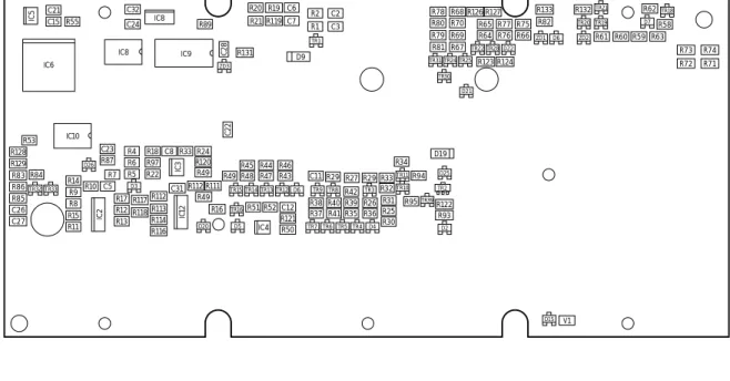
10.1 12V Computers, Type 100 (Q067) and Type 300 (Q068)
R33 R34 R32 R31 R25 R30 R94 R95TR39 TR10 TR11 R122 R93 D2 TR2 D25 D9 R29 TR3 R26 R36 D4 R27 R39 R35 R42 TR4 TR5 TR6 TR7 R40 R41 R38 R37 TR8 TR9 R29 C11 D6 R46 R43 R44 R47 R45 R48 TR12 TR13 TR14 TR15 R49 C12 R121 R50 R52 R51 TR16 D5 IC4 R24 R120 R49 R33 C8 R18 R97 R22 D20 R16 R111 R112 R49 C31 IC 3 IC 12 R112 R113 R114 R116 IC2 R4 R6 R5 D3 R17 R12 R13 R117 R118 D26 C23 R87 R7 C5 R10 IC10 R14 R9 R8 R15 R11 TR33 TR32 R84 R53 R128 R129 R83 R86 R85 C26 C27 IC6 R55 C15 C21 IC5 IC8 R74 D7 R71 R73 R72 TR18 R58 R63 R62 R59 R60 R61 TR19 TR20 R132TR21 ZD2 R133 R82 D6 ZD1 R75 R66 R77 R76 R65 R64 R127 R126 D22 TR28 R124 R123 TR22 D21 TR25 TR24 TR31 TR30 R68 R78 R70 R80 R69 R79 R67 R81 C2 C3 TR1 R2 R1 C6 C7 R19 R119 R20 R21 R131 R89 ZD3 C28 C22 IC9 IC8 C24 C32 D19 V1 D15 D2136-2 TR27 TR23 TR26 TR38 C4 C1 IC7 SK1 C25 C16 C17 C19 C20 C18 RL3 RL2 RL1 LK3 TR29 LK1 IC1 XL1
Figure 10 Circuit Diagram 12V Computers, Type 100 (Q067) and Type 300 (Q068) (See Parts List for differences)
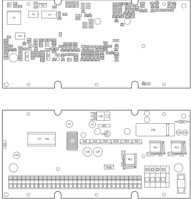
10.2 24V Computer, Type 300 (Q069)
R33 R34 R32 R31 R25 R30 R94 R95TR39 TR10 TR11 R122 R93 D2 TR2 D25 D9 R29 TR3 R26 R36 D4 R27 R39 R35 R42 TR4 TR5 TR6 TR7 R40 R41 R38 R37 TR8 TR9 R29 C11 D6 R46 R43 R44 R47 R45 R48 TR12 TR13 TR14 TR15 R49 C12 R121 R50 R52 R51 TR16 D5 IC4 R24 R120 R49 R33 C8 R18 R97 R22 D20 R16 R111 R112 R49 C31 IC 3 IC 12 R112 R113 R114 R116 IC2 R4 R6 R5 D3 R17 R12 R13 R117 R118 D26 C23 R87 R7 C5 R10 IC10 R14 R9 R8 R15 R11 TR33 TR32 R84 R53 R128 R129 R83 R86 R85 C26 C27 IC6 R55 C15 C21 IC5 IC8 R92 D7 R91 C62 R90 TR18 R58 R63 R62 R59 R60 R61 TR19 TR20 R132TR21 ZD2 R133 R82 D6 ZD1 R75 R66 R77 R76 R65 R64 R127 R126 D22 TR28 R124 R123 TR22 D21 TR25 TR24 TR31 TR30 R68 R78 R70 R80 R69 R79 R67 R81 C2 C3 TR1 R2 R1 C6 C7 R19 R119 R20 R21 R131 R89 ZD3 C28 C22 IC9 IC8 C24 C32 D19 V1 D15 C61 D23 D24 R125 D2137-1 TR27 TR23 TR26 TR38 C4 C1 IC7 SK1 C25 C16 C17 C19 C20 C18 RL3 RL2 RL1 TR29 LK2 C18 XL1 R107 IC13 D18 C34 C29 D1 L110.3 PCB Components, Type 100 12V (Q067) and Type 300 12V
(Q068)
Surface Mount RESISTOR 8R2 5% 125mw R36, 55, 85, 86, 89, 132, 133 RESISTOR 47R 55 125mW R43 RESISTOR 82R 1% 125mw R20 RESISTOR 270R 1% 125mw R8, 9, 82, 119 RESISTOR 390R 5% 125mw R26, 37, 38, 40, 41, 48 RESISTOR 1K0 1% 125mw R6, 7, 10, 11, 21, 111, 131 RESISTOR 1K2 1% 125mw R19, 71, 72, 73, 74 RESISTOR 1K5 5% 125mw R44, 83, 84, 93 RESISTOR 2K2 5% 125mw R27, 35, 50, 67, 69, 79, 81, 121, 122, 128 RESISTOR 4K7 5% 125mw R1, 32, 46, 47, 49, 52, 58, 61, 64, 65, 76, 77, 87, 95, 126, 127, 129 RESISTOR 5K6 1% 125mw R4, 5, 16, 18, 97, 110, 112, 116, 123, 124 RESISTOR 10K 5% 125mw R2, 14, 15, 23, 24, 29, 34, 39, 42, 45, 51, 59, 60, 68, 80, 113, 114 RESISTOR 15K 5% 125mw R30, 66, 70, 75, 78 RESISTOR 22K 5% 125mw R28 RESISTOR 33K 1% 125mw R17, 94, 117 RESISTOR 39K 5% 125mw R25, 31, 33 RESISTOR 68K 1% 125mw R12, 13, 22, 62, 63, 115, 118 RESISTOR 820K 5% 125mW R120 RESISTOR 1M0 1% 125mw R53 CAPACITOR 22nF 5% X7R 1206 50V C3 CAPACITOR 1000pF 2% COG 50V C8 CAPACITOR 1000pF 5% COG 50V C11 83051t5aSurface Mount Type 100 12V (Q067) and Type 300 12V (Q068) (ctd)
CAPACITOR 0.1uF 20% X7R 1206 50V C2, 5, 6, 7, 12, 15, 21, 22, 23, 24, 26,
28, 31, 32, 33
CAPACITOR TANTALUM 2.2uF C27
DIODE SOT23 BAS19 D2, 5, 6, 7, 15, 20, 25, 26
DIODE SOT23 BAV70 D21, 22
DIODE SOT23 BAV99 D4, 8
DIODE SOT23 BAW 56 D3
ZENER DIODE BZX12V ZD1, 2
ZENER DIODE SOT23 BZX6V8 ZD3
RECTIFIER DIODE 1A 100V D9, 19 TRANSISTOR BC807 SOT23 PNP TR3, 12, 32 TRANSISTOR BC817 SOT23 NPN TR1, 4, 5, 6, 7, 8, 9, 10, 11, 13, 14, 15, 16, 18, 19, 22, 24, 25, 28, 30, 31, 33, 39 TRANSISTOR BC868 SOT89 NPN TR2 TRANSISTOR 2N7002 TR20, 21 74HC4051 IC2, 12
DUAL OP AMP TLC272 IC3
OPTO - COUPLER PC317 IC4
EEPROM 9306 IC5
MICROCONTROLLER 80C32 IC6
8 - BIT LATCH 74HC373 IC8
8K RAM HM6264A IC9
8 - BIT LATCH 74HC374 IC10
QUAD 2 - INPUT NOR 74HC02 IC11
VARISTOR VC1206260540 V1
Conventional Components, Type 100 12V (Q067) and Type 300 12V (Q068)
CAPACITOR ELECTROLYTIC 1uF C19, 20
CAPACITOR ELECTROLYTIC 10uF 25V C16, 17
CAPACITOR ELECTROLYTIC 100uF 25V C1, 4, 25
CAPACITOR ELECT’LYTIC 1000uF 63V C18
FET (SEE NOTE) TR23, 26, 27, 29
FET IRF Z34 60V 30A 50MOHM TR38
5V REGULATOR WITH RESET LM2925 IC1
64K EPROM 27C512 200nS IC7
RESONATOR THREE LEGGED XL1
RELAY 12V 40A RL1, 2, 3
FUSE HOLDER 1 off
LINK LK1, LK3
IC SOCKET 28 PIN DIL 1 off
4 - WAY TERMINAL BLOCK 1 off
TERMINAL BLOCK 31 off
TERMINAL BLOCK END PLATE 1 off
LABEL (SEE NOTE) 1 off
83051t5c
NOTE: Type 100 12V Q067: FET IRF Z34 60V 30A 5OMOHM and Red Dot Label
10.4 PCB Components, Type 300 24V (Q069)
Surface Mount RESISTOR 8R2 5% 125mw R36, 55, 85, 86, 89 RESISTOR 10R 1% 125mw R125 RESISTOR 47R 5% 125mW R43, 133 RESISTOR 82R 1% 125mw R20 RESISTOR 270R 1% 125mw R8, 9, 119 RESISTOR 390R 5% 125mw R26, 37, 38, 40, 41, 48 RESISTOR 470R 5% 125mw R90, 132 RESISTOR 1K0 1% 125mw R10, 11, 21, 111, 131 RESISTOR 1K2 1% 125mw R19, 91 RESISTOR 1K5 5% 125mw R6, 7, 44, 83, 84, 93 RESISTOR 2K2 5% 125mw R27, 35, 50, 67, 69, 79, 81, 121, 122, 128 RESISTOR 2K2 5% 125mw R82 RESISTOR 4K7 5% 500mw R1, 32, 46, 47, 49, 52, 58, 61, 64, 65, 76, 77, 87, 95, 126, 127, 129 RESISTOR 5K6 1% 125mw R16, 18, 97, 110, 112, 116, 123, 124 RESISTOR 10K 5% 125mw R2, 14, 15, 23, 24, 29, 34, 39, 42, 45, 51, 59, 60, 68, 80, 113, 114 RESISTOR 12K 5% 125mw R92 RESISTOR 15K 5% 125mw R30, 66, 70, 75, 78 RESISTOR 22K 5% 125mw R28 RESISTOR 33K 1% 125mw R4, 5, 12, 13, 17, 94, 117 RESISTOR 39K 5% 125mw R25, 31, 33 RESISTOR 68K 1% 125mw R22, 62, 63, 96, 115, 118 RESISTOR 820K 5% 125mW R120 RESISTOR 1M0 1% 125mw R53 CAPACITOR 22nF 5% X7R 1206 50V C3 CAPACITOR 1000pF 2% COG 50V C8Surface Mount Type 300 24V (Q069) (ctd)
CAPACITOR 0.1uF 20% X7R 1206 50V C2, 5, 6, 7, 12, 15, 21, 22, 23, 24, 26,
28, 31, 32, 33
CAPACITOR TANTALUM 1uF 16V SIZE A C61, 62
CAPACITOR TANTALUM 2.2uF C27
DIODE SOT23 BAS19 D2, 5, 6, 7, 15, 20, 23, 24, 25, 26
DIODE SOT23 BAV70 D21, 22
DIODE SOT23 BAV99 D4, 8
DIODE SOT23 BAS19 D2, 5, 6, 7, 15, 20, 25, 26
DIODE SOT23 BAV70 D21, 22
DIODE SOT23 BAV99 D4, 8
DIODE SOT23 BAW 56 D3
ZENER DIODE BZX12V ZD1, 2
ZENER DIODE SOT23 BZX6V8 ZD3
RECTIFIER DIODE 1A 100V D9, 19 TRANSISTOR BC807 SOT23 PNP TR3, 12, 32 TRANSISTOR BC817 SOT23 NPN TR1, 4 - 11, 13 - 16, 18, 19, 22, 24, 25, 28, 30, 31, 33, 39 TRANSISTOR BC868 SOT89 NPN TR2 TRANSISTOR 2N7002 TR20, 21 74HC4051 IC2, 12
DUAL OP AMP TLC272 IC3
OPTO - COUPLER PC317 IC4
EEPROM 9306 IC5
MICROCONTROLLER 80C32 IC6
8 - BIT LATCH 74HC373 IC8
8K RAM HM6264A IC9
8 - BIT LATCH 74HC374 IC10
QUAD 2 - INPUT NOR 74HC02 IC11
VARISTOR VC1206260540 V1
Conventional Components, Type 300 24V (Q069)
RESISTOR 270R 5% 500mW R107
CAPACITOR ELECTROLYTIC 1uF C19, 20
CAPACITOR ELECTROLYTIC 10uF 25V C17, 17, 30
CAPACITOR ELECTROLYTIC 470uF 55V C29
CAPACITOR ELECTROLYTIC 100uF 25V C1, 4, 25
CAPACITOR ELECTROLYTIC 1000uF 16V
C34 CAPACITOR ELECTROLYTIC 1000uF
63V
C18
DIODE MR751 D1
DIODE FAST RECOVERY PBYR1645 D18
FET SMP 60N06 - 18 TR23, 26, 27, 29
FET IRF Z34 60V 30A 50MOHM TR38
5V REGULATOR WITH RESET LM2925 IC1
SWITCH MODE REGULATOR LT1270 IC13
64K EPROM 27C512 200nS IC7
RESONATOR THREE LEGGED XL1
INDUCTOR 100uH 8A L1
RELAY 12V 40A RL1, 2, 3
FUSE HOLDER 1 off
LINK LK2
IC SOCKET 28 PIN DIL 1 off
4 - WAY TERMINAL BLOCK 1 off
TERMINAL BLOCK 31 off
TERMINAL BLOCK END PLATE 1 off
BLUE DOT LABEL 1 off