Universität Bonn
Physikalisches Institut
Development of pixel front-end electronics using
advanced deep submicron CMOS technologies
Miroslav Havránek
The content of this thesis is oriented on the R&D of microelectronic integrated circuits for processing the signal from particle sensors and partially on the sensors themselves. This work is motivated by ongoing upgrades of the ATLAS Pixel Detector at CERN laboratory and by exploration of new tech-nologies for the future experiments in particle physics. Evolution of techtech-nologies for the fabrication of microelectronic circuits follows Moore’s laws. Transistors become smaller and electronic chips reach higher complexity. Apart from this, silicon foundries become more open to smaller customers and of-ten provide non-standard process options. Two new directions in pixel technologies are explored in this thesis: design of pixel electronics using ultra deep submicron (65 nm) CMOS technology and De-pleted Monolithic Active Pixel Sensors (DMAPS). An independent project concerning the measurement of pixel capacitance with a dedicated measurement chip is a part of this thesis. Pixel capacitance is one of the key parameters for design of the pixel front-end electronics and thus it is closely related to the content of the thesis. The theoretical background, aspects of chip design, performance of chip proto-types and prospect for design of large pixel chips are comprehensively described in five chapters of the thesis.
Physikalisches Institut der Universität Bonn Nussallee 12 D-53115 Bonn BONN-IR-2014-11 September 2014 ISSN-0172-8741
Universität Bonn
Physikalisches Institut
Development of pixel front-end electronics using
advanced deep submicron CMOS technologies
Miroslav Havránek
aus
Prostˇejov, Czech Republic
Dieser Forschungsbericht wurde als Dissertation von der Mathematisch-Naturwissenschaftlichen Fakultät der Universität Bonn angenommen und ist 2014 auf dem Hochschulschriftenserver der ULB Bonnhttp://hss.ulb.uni-bonn.de/diss_onlineelektronisch publiziert.
1. Gutachter: Prof. Dr. Norbert Wermes 2. Gutachterin: Prof. Dr. Jochen Dingfelder
Angenommen am: 25.08. 2014 Tag der Promotion: 12.09.2014
Contents
1 Introduction 1
2 Pixel detectors for experimental high energy physics 3
2.1 Role of pixel detectors in high energy physics . . . 3
2.2 Tracking systems . . . 4
2.3 Hybrid pixel detectors. . . 7
2.3.1 Pixel sensor . . . 8
2.3.2 Front-end electronics . . . 13
2.3.3 Charge sensitive amplifier . . . 13
2.3.4 Shaper . . . 19
2.3.5 Discriminator . . . 21
2.3.6 Digital logic . . . 22
2.3.7 Interconnection . . . 22
2.4 ATLAS Pixel Detector . . . 23
2.5 ATLAS upgrade. . . 25
2.6 Insertable B-Layer . . . 25
2.6.1 Sensors . . . 25
2.6.2 Front-end chip . . . 26
3 Pixel capacitance and electronic noise 29 3.1 Noise in the charge sensitive amplifier . . . 29
3.1.1 Thermal noise. . . 29 3.1.2 Flicker noise . . . 30 3.1.3 Shot noise. . . 31 3.2 Noise modelling. . . 31 3.3 Noise simulations . . . 32 3.3.1 AC noise simulation . . . 33
3.3.2 Transient noise simulation . . . 33
3.3.3 Noise simulation of FE-I4 . . . 33
3.4 Determination of the pixel capacitance . . . 34
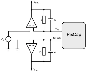
3.5 PixCap. . . 35
3.5.1 Capacitance measurement with PixCap . . . 38
3.5.2 Capacitance of a silicon planar sensor . . . 40
3.5.3 Capacitance of a diamond sensor. . . 44
3.5.4 Capacitance of a silicon 3D sensor . . . 47
3.6 Summary on the capacitance measurement. . . 47
4 New directions in pixel technologies 49 4.1 Motivation. . . 49
4.2.2 Existing prototypes and results . . . 55
4.3 Vertical integration . . . 58
4.3.1 Aspects of vertical integration . . . 58
4.3.2 FE-TC4 . . . 60
4.4 Monolithic Active Pixel Sensors . . . 61
4.4.1 Introduction. . . 61
4.4.2 MAPS fabricated on epitaxial layer . . . 61
4.4.3 High Voltage MAPS . . . 63
4.4.4 High Resistive MAPS . . . 63
4.5 Summary on the future pixel technologies . . . 64
5 Pixel front-end development in 65 nm CMOS technology 65 5.1 Introduction . . . 65
5.2 FE-T65-0 . . . 65
5.2.1 Charge sensitive amplifier . . . 66
5.2.2 Continuous discriminator. . . 66
5.2.3 Dynamic discriminator . . . 67
5.2.4 Measurements with FE-T65-0 . . . 67
5.3 FE-T65-1 . . . 71
5.3.1 Noise . . . 75
5.3.2 Dynamic performance . . . 76
5.3.3 Threshold dispersion . . . 77
5.3.4 Crosstalk . . . 79
5.3.5 Comparison of FE-T65-1 with FE-I4 . . . 80
5.4 Summary of the pixel FE development in the 65 nm CMOS technology . . . 80
6 Depleted Monolithic Active Pixel Sensors 83 6.1 A new concept of the Monolithic Active Pixel Sensors . . . 83
6.2 Technology for fabrication of DMAPS sensors. . . 84
6.3 Test chip EPCB01. . . 84
6.4 Characterization of EPCB01 . . . 88
6.4.1 Gain determination with external charge injection . . . 89
6.4.2 Noise performance . . . 91
6.4.3 Threshold dispersion . . . 93
6.4.4 Cluster size measurement . . . 95
6.4.5 Gain determination using an55Fe - radioactive source. . . 96
6.4.6 Radiation effects in the FE elelctronics of the DMAPS sensors . . . 97
6.5 EPCB02 . . . 99
6.5.1 Variants of the DMAPS pixels . . . 99
6.5.2 Collection electrodes . . . 100
6.5.3 Changes in the FE electronics . . . 101
6.5.4 Monolithic PixCap . . . 101
6.6 Summary of the DMAPS pixels . . . 102
Bibliography 109
List of Figures 113
Chapter 1
Introduction
The invention of the cloud chamber in 1911 by the Scottish physicist C. T. R. Wilson [1] opened the door to the new world - the world of elementary particles. Wilson’s cloud chamber allowed visualiza-tion of the particle tracks coming from the natural radioactivity and from the cosmic rays. The type of the particle could be easily identified by a visual analysis of the particle tracks in the real time. During this exciting time of exploring the unknown domain of the reality, many new particles like for example the muon, pion and positron have been discovered by analyzing the "pictures" recorded from the cloud chambers. C. T. R. Wilson received the Nobel Prize in Physics in 1927 for his invention.
In the early experiments (1960s) at particle accelerators, a modified version of the cloud chamber, a bubble chamber [2], has been extensively used. The bubble chamber is filled with a superheated liquid and contains a piston which allows to make a fast change of the pressure inside the chamber, thus bringing the liquid into a superheated state. As the particles traverse the superheated medium, they vaporize the liquid along their paths. These trails of bubbles were photographed and the films were analyzed manually (see Figure1.1(a-c)). Bubble chambers provide good spatial resolution (severalµm). One of the greatest discoveries made by a bubble chamber was the discovery of the neutral currents in 1973 at the Gargamelle bubble chamber installed at CERN [3]. The inventor of the bubble chamber, D. A. Glaser, was awarded the Nobel Prize in physics in 1960.
Figure 1.1: Photographs of the particle tracks (a) were analyzed manually by human "scanners" (b). Nowadays, the films capturing the "physics data" from 60s-70s are stored in metallic cans in the CERN underground (c) [4]. The path of evolution of the tracking detectors was further oriented towards gaseous detectors like for example spark chambers which allowed triggered operation or Multi Wire Proportional Chambers (MWPC) surpassing the previous generations of the detectors by high detection rates and electronic read-out. History of particle detectors is rich and well beyond the scope of this overview. More
com-prehensive overview of historical development of the particle detectors is shown for example in [5].
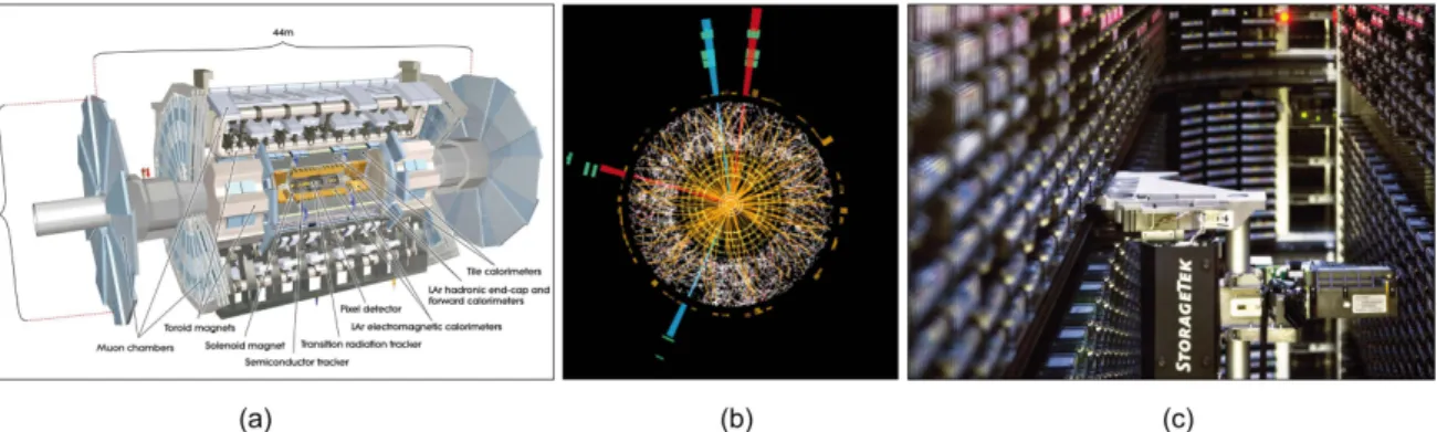
Nowadays, much more complicated experiments are undertaken in the field of particle physics. The experiments are extremely complex, particle collision rate counts in billions collisions per second and the patterns of the particle tracks are so complicated that even the best human "scanner" would never figure out what happened during the particle collisions (see Figure1.2 (a-c)). Large experiments in contemporary high energy physics contain many sub-detectors with an electronic readout, automatically digitizing the particle collision events and storing the data with the rates of gigabytes per second for further analysis. This process is fully computerized.
Figure 1.2: Large particle experiments like the ATLAS experiment at CERN (a) are built to study the physical pro-cesses occurring in the microscopic scales. Complex patterns of the particle tracks (b) are analyzed by computers and the data are stored on magnetic tapes in data storage centers (c) [6], [7].
This thesis is dedicated to the development of pixel detectors, which play a role of tracking and ver-texing devices in the modern experiments in High Energy Physics (HEP). The core of the research work presented in this thesis is a design of Integrated Circuits (IC) in the advanced CMOS technologies and evaluation of their performance for applications in experiments in HEP. The IC design involves con-ceptual studies of the future integrated circuit and translation of the concept to the electrical schematic. Extensive simulations and optimizations of the schematic parameters are made before the layout - phys-ical placement of the transistors and the metallic interconnection can be made. Integrated circuits are fabricated in silicon foundries located only in several places in the world.
Design of several integrated circuits of pixel related electronics, research results and the necessary theoretical background are presented in the following five chapters of this thesis and summarized in the last chapter.
The second chapter (the first chapter is this introduction) gives a theoretical background about pixel detectors with the emphasis on the analog parameters of the pixel front-end electronics. The third chapter discusses the influence of the pixel capacitance on the noise performance of the pixel detector. The main part of this chapter is dedicated to the design of a pixel capacitance measurement chip PixCap and results obtained with this chip. The fourth chapter introduces new technologies in pixel detectors and prepares the ground for the next two chapters. The fifth chapter describes author’s work on a design of the pixel front-end electronics in a 65 nm CMOS technology and discusses the lessons learned with this technology during the design and testing phase of the chip. The sixth chapter is devoted to design and measurements of a new generation of monolithic pixel sensor chip. The thesis finalizes with conclusions.
Chapter 2
Pixel detectors for experimental high energy
physics
2.1 Role of pixel detectors in high energy physics
Experiments in High Energy Physics (HEP) allow to study the composition of matter at the smallest possible scales and examine the laws governing the interactions between the elementary particles. In order to approach distances of the order of 10−19 m, particles are collided at TeV energy scales. Not only energy but also luminosity (a quantity related to the particle collision rate) is an important quantity, particularly in case of studying rare physical processes occurring with a small probability.
The energy frontier particle collider is the Large Hadron Collider (LHC) (see Figure2.1) [8] at CERN particle laboratory near Geneva in Switzerland. LHC was designed to collide protons at center of mass energy of 14 TeV and luminosity of 1034cm-2s-1. Protons are accelerated in bunches of 1011protons. These bunches collide at the collision points every 25 ns, producing about one billion proton-proton collisions every second. More details about the LHC can be found in [8].
Figure 2.1: The Large Hadron Collider has four large experiments: ALICE, ATLAS, CMS and LHCb [9].
Four large experiments are installed at the collision points of LHC: two general purpose experiments ATLAS [9] and CMS [10], an experiment dedicated to studies of heavy ion collisions - ALICE [11], and an experiment optimized for studying the b-physics - LHCb [12]. These experiments measure parameters of secondary particles produced in the collisions of the high energetic primary particles. In order to precisely measure trajectories and origins (vertices) of these secondary particles, the tracking detectors are situated very close to the collision point. Tracking and vertexing detectors are finely seg-mented silicon pixel or strip detector systems with short recovery time and high data throughput. All large experiments (except ALICE, which uses Time Projection Chamber) use silicon tracking systems. Technological progress in the past 20 years allowed design of silicon detectors with the size of sensitive cells of the order of tens of microns, which outperform the older generation of gas detectors in terms of speed and spatial resolution.
Currently, two large pixel detectors operate in the experiments ATLAS [6] and CMS [13]. In spite of operation in a hostile radiation environment, the pixel detectors provide data allowing the reconstruc-tion of events with multiple vertices (see Figure2.2) with unprecedented precision. The technology of pixel detectors significantly improved the precision measurements in particle physics and finally played a crucial role in the discovery of the Higgs boson at these experiments in 2012 [14], [15].
Figure 2.2: Example of a candidate event of Zboson decaying intoµ+µ− recorded by the ATLAS experiment [16]. This event contains 25 reconstructed vertices.
2.2 Tracking systems
The tracking system (tracker) is an essential component of a large HEP experiment. The tracker per-forms a precise measurement of particle trajectories. Electrically charged particles are detected in sens-itive layers of the tracker. Throughout this thesis we will often refer to the coordinates of the coordinate system in which the tracker is placed. Definition of the coordinatesx, y,z, φ, θandηis identical with the ATLAS experiment and can be found in [6].
The sensitive layers of a tracker are usually arranged as coaxial (with respect tozaxis) barrel layers and several end-cap disks to provide a broad angular coverage. Trackers operate in a strong magnetic oriented alongz axis. The magnetic field curves the particle trajectories proportionally to their mo-mentum as shown in Figure2.3(a). By measuring the curvature of the trajectory, the momentum of the particle is determined.
2.2 Tracking systems
In case of a tracker consisting of three sensitive tracking layers placed inside a solenoidal magnetic field, we can express the transverse momentumpT of the particle in terms of two geometrical quantities Land s (sagitta) as described in Figure2.3 (b) and the strength of the magnetic field alongz axis Bz
(more detailed derivation can be found in [17]):
pT =
0.3BzL2
8s (2.1)
Momentum resolution is then given by formula:
σ(pT) pT = r 3 2σx 8pT 0.3BzL2 (2.2)
Momentum resolution improves quadratically with the radius of the tracker and linearly with the magnetic field and degrades with increasing transverse momentum and uncertainty of the spacepoint measurementσx of the sensitive elements. The spacepoint resolution of the tracking layers is directly
related to the geometry of the sensitive elements and cluster size. In order to find the optimum para-meters of a tracker providing the best momentum resolution, additional quantities must be taken into account, for example the granularity of the sensitive layers, the inserted material causing multiple scat-tering and the financial budget.
Figure 2.3: (a): Trajectories of the charged particles are curved due to the magnetic field. By measur-ing the curvature radius of the trajectory, transversal momentum of the particle can be determined. (b): Transversal momentum is often expressed in terms of sagitta (s) and distance between spacepoints (L). Although a large radius tracker is useful for the momentum measurement, some experimental meth-ods require the determination of a decay point (vertex) of short lived particles as for example B mesons, D mesons or Λ baryons which fly only a fewµm before they decay. The position of the vertex is measured by a vertex detector. The vertex detector contains finely segmented pixellated layers closely surrounding the collision point, thus allowing a precise measurement of the vertex position and the im-pact parameters of the tracks (see Figure2.4).
Figure 2.4: Short lived particles travel just a few tens ofµm and decay before they reach the detector. In this case a displaced (secondary) vertex is observed in the detector. The tracks, ori-ginating at the secondary vertex, are described by transversal (d0) and longitudial (z0) impact parameters.
The vertex resolution can be derived from a simple model described in [18]. If we assume a two layer vertex detector with a geometry described in Figure2.5having the spatial resolutionσ1 in layer 1 and
σ2in layer 2, the resolution of the vertex position is a quadratic sum of terms arising from spacepoint uncertaintiesσ1andσ2as follows:
σV X = q σ2 V X1+σ 2 V X2 (2.3)
whereσV X1andσV X2are functions of the vertex detector geometry and the spatial resolution of the detector elements: σV X1= R2 R2−R1σ1 σV X2= R1 R2−R1σ2 (2.4)
The quantities R0 andR1 andR2 are radii of the beam pipe and the sensitive layers. The particles passing the beam pipe are scattered and thus deflected by an angleθwith uncertaintyσθ. Correction for
multiple scattering enters the formula for vertex resolution in the following way:
σ2
1→σ21+(R1−R0)2σ2θ (2.5)
σ2
2→σ21+(R2−R0)2σ2θ (2.6)
The multiple scattering terms entering σ1 andσ2 are correlated. Assuming 100% correlation, we obtain following formula for the vertex resolution:
σV X = σ2 1R22+R21σ22 (R2−R1)2 +σ 2 θ(R2(R1−R0)+R1(R2−R0))2 (2.7) Multiple scattering occurs also in the tracking layers and the model becomes more complicated. An alternative way to determine the vertex resolution is by performing a Monte Carlo simulation.
2.3 Hybrid pixel detectors
Using this simplistic model we can see that a good vertex resolution will be achieved if the distance between layer 1 and layer 2 is large, layer 1 is as close to the interaction point as possible, the beam pipe is as thin as possible and the spacepoint resolution of the sensitive layers is as high as possible.
Figure 2.5: Geometrical model of a vertex detector for determ-ination of the vertex resolution.
2.3 Hybrid pixel detectors
Hybrid pixel detectors are widely used in HEP for tracking and vertexing. Vertex detectors using this technology have been successfully implemented in experiments at the LHC: ATLAS [19], CMS [13] and ALICE [20]. Hybrid pixel detectors are distinguished by their excellent spatial resolution (fine seg-mentation), low noise, radiation hardness, fast read-out and small inserted mass in the detector.
A hybrid pixel detector is a composition of sensor and read-out chip interconnected by a suitable technology (see Figure 2.6). This approach allows an independent development of these components and more freedom in design and fabrication. On the other hand, the interconnection process represents a significant portion of a financial budget for the detector production. In the following sub-sections we will describe sensor and front-end electronics in more detail.
Figure 2.6: A hybrid pixel detector consists of a sensor and a front-end electronic chip interconnected by the bump and flip-chip technology.
2.3.1 Pixel sensor
Pixel sensors for applications in HEP are predominantly made of silicon. Silicon is a favorable material due to its relatively small band-gap of 1.1 eV with respect to the ionisation energy of the older genera-tion of gaseous detectors (typically more than 10 eV), and therefore, silicon sensors provide a relatively large signal. From the technology point of view, silicon is readily available and sensor fabrication pro-cess is compatible with the propro-cesses for fabrication of microelectronics.
HEP applications typically require detection of highly energetic particles passing the sensors without loosing a significant fraction of their initial kinetic energy. The silicon sensor is sensitive to electrically charged particles as for example electrons, muons, pions, kaons and others. The dominant physical pro-cess of interaction of these particles with the sensor is ionisation accompanied by creation of electron-hole (e-h) pairs in the sensor. The energy needed for the creation of a single e-h pair in silicon is on average 3.65 eV.
The mean energy, deposited in the sensor by a heavy relativistic charged particle, is described by Bethe-Bloch formula [21]: − * dE dx + =Kz2Z A 1 β2 " 1 2ln 2mec2β2γ2Tmax I2 −β 2−δ(βγ) 2 # (2.8)
Ionization energy loss of a charged particle passing the matter depends on parameters of the incident particle (mass, velocity, electric charge) and on the properties of the material. Meaning of the variables used in the Bethe Bloch formula is explained in Table2.1. Tmaxis maximum kinetic energy transfer of
the incident particle to the electron during a single collision. The value ofTmaxarises from the laws of
conservation of energy and momentum and is described here:
Tmax=
2mec2β2γ2
1+2γme/M+(me/M)2
(2.9)
Symbol Definition Units
K 4πNAr2emec2 0.307 075 MeV mol−1cm2
NA Avogadro’s number 6.022 141 29(27)×1023mol-1
re2 e2
4π0mec2 (elelctron radius) 2.817 940 3267(27) fm e electron charge (abs. value) 1.602×10⁻¹⁹C
0 permittivity of vacuum 8.85×10⁻¹²F
mec2 rest energy of electron 0.5109958918 (44) MeV
M mass of the incident particle MeV
z charge number of incident particle
Z atomic number of absorber
A atomic mass number of absorber g·mol−1
I mean excitation energy eV
δ(βγ) density effect correction to ionization energy loss
2.3 Hybrid pixel detectors
Figure 2.7: Radiation loss of a heavy charged particle (muon) in matter (copper) [21].
As shown in Figure2.7, the Bethe Bloch formula describes the ionisation energy loss of muons in broad range of energies. Similar characteristic can be computed for other particle types and energy absorbing materials. The energy, deposited by the process of ionisation is a subject of large fluctuations with a characteristic long tail towards high energy, described by the Landau distribution.
Three conditions must be satisfied in order a piece of silicon can be used as a particle sensor:
1. silicon must be free of impurities which can eventually become charge generation or recombina-tion centers
2. the bulk of the sensor must be free of charge carriers (must be either depleted or intrinsically free (diamond))
3. a drift field must be present in the sensor
The first condition is met by using high resistivity (several kΩ·cm) silicon often doped with oxy-gen atoms to increase radiation hardness. The second and third conditions are met in an array of PN junctions (diodes) technologically processed on the high resistivity silicon and biased with high voltage oriented in the reverse direction of the PN junctions.
A PN junction forms at the p-n boundary in the semiconductor material separating the two regions of different types of conductivity: p-type (positive) conductivity is accomplished by holes originating from a non-saturated atomic bonds of acceptor atoms (B, Al); n-type (negative) conductivity is accomplished by electrons due to doping by donor atoms (P, As). A schematic cross section of a PN junction is shown in Figure2.8. In the vicinity of the PN junction a depletion region forms due to diffusion of holes from the p-doped region into the n-doped region and diffusion of electrons from n into p.
Figure 2.8: Cross section of a PN junction. Majority charge carriers diffuse across the PN junction and recombine on the other side of the junction and thus a depletion region around the PN junction is formed.
Diffusion current densities j of electrons and holes are proportional to the gradient of the dopant concentrationn: jn=−Dn∇nn=− kT e µn∇nn (2.10) jp=Dp∇np= kT e µp∇np (2.11)
whereDis the diffusion constant,kthe Boltzmann constant,Tis an absolute temperature andµstands for the mobility of the charge carriers. The charge carriers which already crossed the PN junction re-combine and are no-longer free. These trapped charges build up an electric field across the PN junction and create a potential wall between p and n regions. The shape of the electric field and the potential around the PN junction can be obtained by solving the Poisson equation. The electric potentialφand the electric fieldEacross the PN junction are illustrated in Figure2.8.
The width of the depletion regionWdepends on the concentration of charge carriers and also on the bias voltage (Vbias) of the sensor according to the formula:
W= s 20S i e 1 nn + 1 np ! (Vbias+Vbi) (2.12)
0 is the vacuum permittivity andris the relative permittivity of silicon. Vbi is the built-in voltage
2.3 Hybrid pixel detectors
the concentration of the dopants is not equal on both sides of the PN junction. The bulk of the sensor is usually much less doped than the biasing electrodes and collecting electrodes. Bias voltage of the sensor is of the order of 100 V and the build-in voltage about 0.5 V. Hence equation2.12can be simplified:
W= r 20S i e 1 nbulk Vbias (2.13)
In this case, the depletion region does not grow to the same depth d on the both sides of the PN junction, but the charge from the highly doped region diffuses further into the low doped region as described by the following formula:
nn·dn =np·dp (2.14)
dnanddpdenote the depth of the depleted layer on each side of the PN junction. The depletion region
broadens with increasing reverse voltage across the PN junction. After reaching a certain bias voltage, the depletion region extends across the entire sensor bulk and can not grow further. At this point we say that the sensor is fully depleted. Using (2.13), the voltage to achieve full depletion of the sensor is proportional to the concentration of the impurities in the silicon bulk and is quadratically proportional to the sensor thickness:
Vf ullDep=
e·nbulk·d2
20S i
(2.15)
Satisfying these the conditions (silicon purity, absence of free charge carriers and presence of electric drift field) the charge, generated by the traversing charged particle, moves under the electric drift field and is collected at the collection electrodes of the sensor. More theoretical details about silicon sensors can be found in [22], [23].
An example of silicon particle sensor used in the ATLAS pixel detector is shown in Figure2.9. In-formation about ATLAS pixel sensors are taken from [19]. The pixel sensor was fabricated on the oxygenated n-type FZ (Float Zone) silicon substrate with thickness of 256µm. The pixel size is defined by the pattern of charge collecting n+regions on the front-side of the sensor. This pixel sensor type is n+ in n. Pixel dimensions are 400×50µm2. The n+regions are separated by p-type regions (p-spray) pre-venting from ohmic connection between n+regions and thus from radiation induced currents between pixels. Back-side of the sensor contains a p+region forming a PN junction. This region is biased by negative sufficiently high voltage to achieve full depletion. The depletion region of the sensor grows (before irradiation) from the back side towards the front-side. The edge of the sensor often contains a significant damage of the crystal lattice and therefore it is conductive. High voltage from the back side of the sensor can therefore easily appear at the edge of the front side thus building up large a electric field, which can lead to an excessive leakage current or break down of the sensor. The back side of the sensor contains several guard-rings which smoothly adjust the potential from the high voltage p+region down to the ground potential of the sensor front-side.
Another class of silicon sensors are 3D sensors [24]. Unlike the planar sensors, the charge collecting electrodes in 3D sensors penetrate the entire sensor bulk. A schematic cross section of a 3D sensor is shown in Figure 2.10 (a, b). This sensor topology has several advantages with respect to the planar sensor. The biasing and charge collecting electrodes are closely spaced and therefore a lower bias voltage is needed to achieve full depletion (see 2.15). A typical bias voltage of the 3D sensor is only about 20 V and after irradiation no more than 200 V, while for planar sensors it is typically 100 V before
Figure 2.9: Cross section of a silicon pixel sensor of n+on n type. Charged particles passing through the sensor creates a number of electron-hole pairs which drift towards the corresponding electrodes in the electric field.
irradiation and 600 V after absorbing a large radiation dose. After charge generation, the signal travels smaller distance to the electrodes (see Figure2.10) and therefore it has smaller probability to be trapped by radiation induced bulk damage. 3D sensors are therefore potentially radiation harder than planar sensors. Another benefit comes from the small distance between the sensitive area of the sensor and its edge. This is achieved by an active edge implant. A disadvantage of vertically arranged collecting electrodes is large pixel capacitance and large insensitive volume of the sensor due to the charge collect-ing and biascollect-ing electrodes. The fabrication process of 3D sensors is more complicated than of planar sensors because it consists of many successive steps involving Deep Reactive Ion Etching (DRIE). The number of companies able to produce 3D sensors is therefore limited.
Figure 2.10: (a): Cross section of a 3D silicon sensor. Charge collecting electrodes are arranged in the form of pillars passing through almost the entire sensor bulk [25]. (b): Comparison of planar and 3D sensors. In the 3D sensor, the signal charge drifts only a short distance towards the collecting electrodes, while in the planar sensor the charge has to travel through substantial part of the silicon bulk [25].
2.3 Hybrid pixel detectors
Except silicon, another interesting material for producing sensors for HEP experiments is diamond. Due to the large band-gap (5.5 eV), diamond is a nearly perfect insulator and diamond crystal can therefore work as a sensor without any further doping. To extract the signal charge, only the pattern of metallic electrodes is needed to generate the drift field. The energy needed to create an electron-hole pair is 13.1 eV on average. Therefore, diamond sensor produces smaller signal with respect to the silicon sensor of the same thickness. Stronger crystal lattice of the diamond sensor predetermines this material for fabrication of radiation hard sensors. Energy needed to release a carbon atom from diamond lattice is 43 eV, while in the case of silicon it is only 25 eV. Application potential of diamond sensors is in the fields requiring a large radiation tolerance. A diamond sensor is not just an "academic option", but is already used for example in the Beam Condition Monitor (BCM) [26] and Diamond Beam Monitor (DBM) [27] in the ATLAS experiment.
2.3.2 Front-end electronics
As we have seen in the previous subsection, silicon sensors provide a typical signal in the range of tens of thousands of electrons within the collection time of a few nanoseconds. Front-end (FE) electronics processes the signal from the sensor. Signal processing starts with the conversion of the signal charge into voltage which is performed by a charge sensitive amplifier (CSA). This voltage is discriminated and digitized. The resulting data are then coded into a comprehensive data format so that information about pixel address, time and amplitude can be disentangled from the data pattern. Then data are transmitted out of the detector.
FE electronics together with the sensor itself define properties of the entire pixel detector as for ex-ample: signal to noise ratio, maximum allowable hit-rate, radiation hardness and power consumption. Special requirements for HEP applications do not allow to use commercially available integrated cir-cuits for signal processing and therefore FE electronics is usually implemented by Application Specific Integrated Circuits - ASICs. The design of an ASIC allows to maximally optimize the performance of the circuitry to the particular application. A general scheme of the FE integrated circuit (FE chip) of a hybrid pixel detector is illustrated in Figure2.11. The core of the chip contains in-pixel FE electronics which is usually identical for every pixel and replicated all over the pixel matrix. The in-pixel electron-ics contains CSA, shaper, discriminator, digital logic and sometimes also DACs for local tuning of pixel parameters. Circuits responsible for fast data transmission - LVDS drivers, global DACs, clock signal generator (PLL), voltage regulators and digital coders (Hamming code to increase bit error immunity) stand at the chip periphery. The following four sub-sections are devoted to the description of CSA, shaper, discriminator and digital logic.
2.3.3 Charge sensitive amplifier
Charge Sensitive Amplifier (CSA) is an electronic circuit converting the electric chargeQto the voltage
Vout. The core of the CSA is a voltage amplifier (core amplifier) providing high open loop gaina. The
voltage amplifier has a capacitive feedbackCf. In the ideal case, the CSA behaves as an integrator
with a closed loop gain (the word gainin the rest of the thesis means always closed loop gain unless otherwise stated)ginversely proportional to the feedback capacitance. The output voltage is related to the input charge as follows:
Vout = Q Cf ; gideal= 1 Cf (2.16)
Figure 2.11: A general scheme of the pixel FE chip. One pixel FE channel contains charge sensitive amplifier, shaper, discriminator and pixel logic.
In the real life, the core amplifier has a finite open loop gain (several hundreds), the capacitance of the sensorCd can be several hundreds of fF. Taking these effects into account, the formula for gain of
the CSA changes to:
g= 1 Cf + Cd+Cf a =gideal· 1 1+ 1a+CCd fa (2.17)
Assuming realistic values of the sensor capacitance of 250 fF, open loop gain of 400 and feedback capacitance of 5 fF, the ideal gain is reduced by a factor of 0.89. Therefore, low detector capacitance and high open loop gain of the core amplifier is desirable.
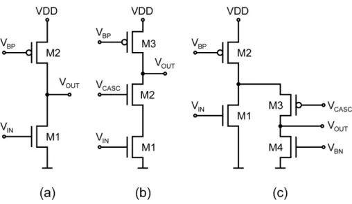
The core amplifier can be implemented in several ways. The most common amplifiers are described in Figure2.12(a-c). The first option is a common source amplifier (Figure2.12(a)). An advantage of this amplifier is its simplicity and the fact that the output potential is similar to the input potential at the transistor M1. Therefore, DC feedback can be easily applied. The gain of this amplifier is equal to:
g=gm·(Ro1||Ro2) (2.18)
Ro1||Ro2is a parallel combination of output resistances of transistor M1 and M2 andgmis the
transcon-ductance of the transistor M1. Typically in deep submicron CMOS technology the output resistances of M1 and M2 are in the range of several MΩand transconductance of the input transistor is in the order of 10 µS. The open loop gain of the common source amplifier rarely exceeds 100 which is the main disadvantage of this architecture. The open loop gain can be enhanced by cascoding the input transistor. This amplifier is called the cascode amplifier and is shown in Figure2.12(b).
Cascoding of the input transistor increases the output resistance of the amplifier and therefore in-creases its gain. If we neglect the body effect of the transistor M2 and assume that (Ro1andRo2)<<Ro3:
g=Ro1gm1(1+gm2Ro2)≈gm1gm2Ro1Ro2
2.3 Hybrid pixel detectors
Figure 2.12: Typical implementations of the core amplifier of the CSA: (a) common source stage, (b) telescopic cascode, (c) folded cascode.
effectively reduces the Miller effect. The cascode amplifier works up to higher frequencies compared to the common source amplifier. On the other hand, the large output resistance only allows loading the amplifier with a high resistance load. The fact that all transistors must operate in saturation limits the maximum output voltage swing of the cascode amplifier.
The input transistor of the amplifier can be also cascoded by a transistor of a different type. In this case we talk about a folded cascode which is shown in Figure2.12(c). An advantage of the folded cascode is that a quiescent DC voltage at the input is similar to that at the output. Therefore, this amplifier is more suitable for closing a DC feedback loop. However, folded cascode requires a higher bias current with respect to the telescopic cascode of a similar performance and therefore this amplifier is less suitable for low power applications. Another option is represented by a differential amplifier. Its advantage is a higher Power Supply Rejection Ratio (PSRR) and Common Mode Rejection Ratio (CMRR) compared to the single-ended architecture. However, the differential amplifier fills a larger silicon area, consumes more power and suffers from a higher noise than the equivalent single-ended amplifier.
Up to now, only the static parameters of the CSA have been discussed. Dynamic parameters of the CSA are crucial in pixel detectors processing large hit rates. Every CSA has a reset circuit to avoid sat-uration after detection of several particles. The reset can be implemented either by a resistor (resistive reset), a switch (switched reset CSA) or by a current source (continuous reset CSA) connected in the feedback loop of the CSA. These options are shown in Figure2.13.
Resistive reset provides an exponential discharge of the CSA with a time constant:
τf =RfCf (2.19)
As we have shown upper in this section, the value of the feedback capacitance (Cf) determines gain
of the CSA and it can not be chosen arbitrarily. Its value is, depending on the signal charge, in the range from 4 fF to 20 fF. The discharge time constant of the CSA in a pixel detector is usually chosen as a compromise between speed (shorterτf, the higher hit-rate the CSA can process) and noise (longerτf,
Figure 2.13: The CSA with different discharge circuits: (a) the CSA with resistive feedback dis-charges exponentially with time constantτf = RfCf. (b) the switched feedback CSA discharges
within a short reset period when the feedback switch is switched on. (c) the CSA with constant current feedback discharges linearly with time.
the better noise performance is achieved). Typical value forτf is between 100 ns and 1µs. In order to
achieve this range of discharge time, the feedback resistor must be very large (∼100 MΩ) which is diffi -cult to realize in CMOS technology. A MOSFET transistor biased in the linear region can perform this task. The second option is a switched reset which is particularly suitable for applications with emphasis on speed. The amplifier with switched reset has faster risetime, no ballistic deficit (described below) and provides fast return to the baseline. The third option is using a current source as a discharge circuit. In this case, the feedback capacitor discharges linearly and the signal amplitude can therefore be measured by a Time Over Threshold method.
Two major effects influence the dynamic performance of the CSA: risetime and ballistic deficit. The risetimeτr of the CSA describes how fast the voltage at the output of the CSA reaches its maximum
value after charge collection (charge collection is assumed to be much shorter thanτr). The ballistic
deficit appears in the CSA with feedback circuit implemented either with a resistor or with a current source. During the timeτr, the CSA already starts being discharged by the feedback circuit limiting the
maximum achievable peak voltage of the CSA. The effect is more significant when theτris of the same
order asτf and the CSA charge collection rate becomes comparable with the discharge rate.
To investigate the dynamic performance of the CSA, a simple model has been used. The model and subsequent analysis was inspired by [28] and that document contains a more detailed description of the CSA. A simplified schematic of the CSA is shown in Figure2.14. The core amplifier with open loop gainais followed by a unity gain buffer. The capacitorCdrepresents sensor capacitance,Rf andCf are
feedback components andCout is the output capacitance of the core amplifier. TheCout capacitor has
been added after the core amplifier rather than after the buffer, because the core amplifier has usually large output resistance and is more sensitive to the load impedance than the buffer. For small signals, this model can be linearized and expressed in more suitable form for the further anlysis as shown in
Fig-2.3 Hybrid pixel detectors
ure2.15. In this model, we assume that the core amplifier is implemented with a single stage amplifier whose gain is given by a product ofgm of the input transistor and output resistance of the amplifying
stageRo.
Figure 2.14: Model of the CSA.
Figure 2.15: Small signal linearized model of the CSA.
Applying the nodal analysis on the linearized model shown in Figure2.15, we obtain the following transfer function:
H(p)= K· (p+Zero)
(p+Pole1)·(p+Pole2) (2.20) The transfer function has one zero (Zero), two polesPole1 andPole2 and a constant factorK. These parameters were computed in Wolfram Mathematica [29] using the assumptionsa1 andCout Cf
as follows: K= aτf gm(aCgoutτd m +τfτout) ; Zero=−gm Cf (2.21) Pole1= gm(τd+aτf +τout) aCoutτd+gmτfτout ; Pole2= τ a d+aτf +τout (2.22)
Time constants and gain are defined in a following way:
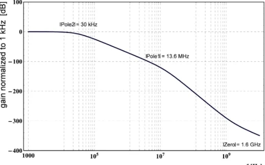
Typical values for the CSA model from Figure2.15are written in Table2.2and the corresponding frequency characteristic is shown in Figure2.16. The poles are located at frequencies of 30 kHz and 13.6 MHz. Each pole bends the frequency characteristic downwards with the rate of 20 dB per decade, while the zero bends the frequency characteristic upward at the frequency of 1.6 GHz by 20 dB per decade. Symbol Value Cd 150 fF Cf 5 fF Rf 1 GΩ gm 50µS Ro 10 MΩ Cout 20 fF
Table 2.2: Typical parameters of the CSA designed in deep sub-micron CMOS technology.
Figure 2.16: Typical frequency characteristic of a CSA designed in deep submicron tech-nology.
Response of a CSA to a Dirac impulse is given by the inverse Laplace transform of the original transfer function (2.20):
Vout =K·
Pole1−Zero Pole1−Pole2·e
Pole1·t+ Zero−Pole2 Pole1−Pole2 ·e
Pole2·t
!
(2.24)
2.3 Hybrid pixel detectors
andPole2at 30 kHz determines a slow CSA discharge. The risetime of the CSA is then proportional to the inverse value of Pole1 and by keeping the most significant terms only, the risetime τr can be
expressed in the following way:
τr≈ 1 Pole1 = aCoutτd+gmτfτout gm(τd+aτf +τout) ≈ Cout·Cd gm·Cf (2.25)
In order to achieve fast risetime, the input transistor must have large transconductance and a large feedback capacitor while the sensor and loading capacitance of the amplifying stage of the CSA must be as small as possible. However, each of these parameters have a direct impact on noise (or rather signal to noise ratio) of the CSA and therefore must be carefully optimized. A very fast CSA is not always the best choice. The charge collection time can be as long as several ns. If the CSA risetime is shorter than the charge collection time, it will not improve the speed of the detector and in addition introduces a higher noise level. The discharge time (or return to baseline) of the CSA is given byPole2
and is approximately equal toτf.
In practice it is desirable thatτf τr. Ifτf is too close toτr (Pole2 approachesPole1), the CSA
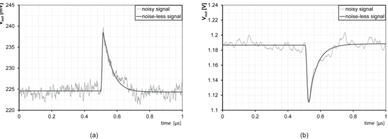
starts discharging before the voltage amplitude at the output of the CSA develops due to the ballistic deficit effect and thus the gain of the CSA drops. A response of the modelled CSA to various input charges is shown in Figure2.17(a) and the effect of the ballistic deficit is shown in Figure2.17(b).
Figure 2.17: (a): Response of the modelled CSA to various input charge amplitudes. Pole2 is set to 30 kHz andPole1 to 13.6 MHz. The characteristic exponential discharge is apparent. (b): ThePole2 is swept close to thePole1 while the injected charge is constant (20 ke-). Decline of the peak voltageV
out is observed due to the
ballistic deficit.
2.3.4 Shaper
A shaper is an electronic filter, usually a band-pass, defining the bandwidth of the signal output of the CSA. The shaper helps to suppress the low and high frequency noise component and therefore improves the signal to noise ratio of the pixel detector. The low fcmin and high fcmax frequencies of the shaper
have to be chosen carefully to optimize Signal to Noise Ratio (SNR). The simplest shaper is the CR-RC filter as shown in Figure2.18.
Figure 2.18: A simple realization of the shaper with CR and RC elements.
The transfer function of this circuit has the form:
H(p)= pC1R1
(1+ pC1R1)(1+pC2R2)
(2.26)
and an example of frequency characteristic with fcmin=fcmax=1 MHz is shown in Figure2.19.
1000 104 105 106 107 108 109 -200 -150 -100 -50 0 f@HzD a @ dB D Frequencycharacteristicof CR-CR filter
Figure 2.19: Frequency characteristic of the CR-RC filter with fcmin= fcmax=1 MHz
The first order CR-RC filter often does not provide a good band-selectivity and therefore filters of higher orders are applied - for example CRn-RCm. Although applying a dedicated shaper in a pixel
read-out chain may be beneficial to improve the SNR, it is often omitted due to various reasons. In HEP, the useful signal usually lies within a bandwidth around 1 MHz and the filter has to be designed accordingly. In the example described above, the time constant is in the range ofµs. This corresponds for example to a resistor in the range of MΩand a capacitor of pF range. Such resistors and capacitors
are often hard to integrate in a small pixel area. In the current trend of decreasing the pixel size and power consumption, the power saving is the next parameter to be considered. In pixel FE electronics, the constant current feedback acts as a filter and by appropriate choice of the discharge time constantτf
2.3 Hybrid pixel detectors
2.3.5 Discriminator
The discriminator stands at the end of the analog read-out chain. The discriminator compares the voltage at the output of the shaper (or CSA) with a reference value and sets its output either to HIGH level or LOW level depending on whether the input voltage is above or below the detection threshold, thus providing digitization with a single bit resolution. If the discriminator processes a signal from the CSA with a constant current source feedback, the length of the pulse at the output of the discriminator is dir-ectly proportional to the signal charge. The length of the pulse can be used for amplitude measurement. This method is called Time Over Threshold and can be understood from Figure2.20.
Figure 2.20: Pulse length at the output of dis-criminator can be used for measurement of signal charge.
Three figures of merit define the performance of the discriminator. High pixel occupancy is typical for high luminosity hadron colliders. The analog read-out chain has to provide information about a hit within a fraction of a microsecond independently of the signal amplitude. Therefore, a high speed discriminator providing a small time-walk of the pixel analog read-out chain is desirable. The second parameter is the dispersion of a voltage input offset of the discriminator across the pixel matrix. Due to fabrication process variations, an offset of the discriminator can significantly change from pixel to pixel. This effect can be compensated by an in-pixel DAC to achieve uniform threshold of all pixels in the matrix. A last, but not least requirement is a low power consumption which goes against the speed requirements. In the pixel electronics, a power of only fewµW is available to power the discriminator. Alternatively, the signal can be digitized by an ADC and discriminated on data level. However, integra-tion of a fast ADC might be challenging and may significantly increase the power budget of the pixel.
2.3.6 Digital logic
A hit of an event is usually stored locally in a pixel waiting for the read-out to be triggered. The event must be assigned with a pixel address and timestamp (bunch crossing ID). An optimal read-out architec-ture strongly depends upon the hit occupancy and bunch crossing scheme. For example, at the LHC the bunch crossings come with the time spacing of 25 ns. It is not possible (and also not needed) to always read-out all pixels at every bunch crossing. The discriminator in a pixel automatically provides a zero suppression and only pixels with a hit are read-out. Large particle experiments like ATLAS or CMS use sophisticated trigger systems which tells the pixel detector to only read-out data when the event is physically interesting. The trigger system needs a time of 2-3µs (trigger latency) for the decision whether the event was interesting or not. The information about the hits must be stored in the pixels for that time before it is either read-out or lost.
Layout of a pixel matrix in a large pixel chip is usually organized in double column regions. This topology is advantageous in terms of distribution of digital signals and separation of the sensitive analog part from the digital part. The data from the pixels are transmitted on a data bus which is common for all pixels in the double column. Data from all double columns are processed by a double column logic and read-out by high speed (for example LVDS) interface.
2.3.7 Interconnection
Interconnection of the sensor and FE electronic chip requires a technology able to deal with a small pitch and high density connections. Several techniques can be used for interconnecting the sensor and the FE chip as for example bump bonding [30], gold stud [31], slid [32], etc. A widely used technology in high energy physics is bump bonding using electroplated solder bumps. More details about chip-to-sensor interconnection are written in [22] and about its capabilities in [33].
Figure 2.21: In the process of bump-bonding, the cylinders of solder bumps (a) are galvanically grown on the silicon chip. After reflow, the solder balls (b) are formed [33].
Bump-bonding is performed within several technological steps involving the deposition of an Under Bump Metallization (UBM), typically containing a thin adhesion layer (Ti/W) and a thick wettable Cu layer. On the top of the UBM the solder (PbSn) cylinders are galvanically grown as shown in Figure2.21 (a). The solder cylinders turn into solder balls under surface tension during reflow at a
2.4 ATLAS Pixel Detector
temperature of about 250oC as shown in Figure2.21(b). The UBM layer is also grown on the surface of the sensor counterpart. Both parts of the detector are then combined and reflown again. This process is called flip-chipping. During the reflow, the surface tension of the solder balls perfectly self-aligns the sensor and the FE chip and minimizes the number of imperfectly connected pixels. This interconnection method provides a mechanically stable connection. A disadvantage of this interconnection technology is its complexity and high cost.
2.4 ATLAS Pixel Detector
The pixel detector [19] is an innermost part of the ATLAS tracking system and is schematically shown in Figure 2.22. Three coaxial barrel layers with radii from 50.5 mm to 122.5 mm and three end-cap disks provide full angular coverage in the φdirection and in θdirection up to η ≤ 2.5 (for definition of coordinates see [6]). The pixel size is 400µm inzdirection and 50µm inφdirection and provides an impact parameter resolution better than 15µm inφdirection and about 1 mm inzdirection. This extraordinary resolution is particularly important for the identification of multiple primary vertices and precision measurement of displaced secondary vertices. A direct consequence of the high resolution is a large number of pixels, about 80 million (67 mil. barrel layers and 13 mil. end-cap disks). The pixel detector was designed to operate in a trigger based data taking mode. Components of the pixel detector have been designed to withstand a radiation dose of about 500 Mrad and a fluence of> 1015 neq/cm2. The entire detector consists of a mechanical support, power and data cables, cooling systems and pixel modules. All the mechanical components of the detector introduce an unwanted multiple scattering of the particles leaving the collision point. Therefore their mass must be as small as possible.
Figure 2.22: A schematic view of the ATLAS pixel detector [19].
The pixel detector contains in total 1744 pixel modules (1456 barrel and 288 end-cap modules). One pixel module is shown in Figure2.23. Each module carries 16 front-end chips FE-I3 [19] bump-bonded to the pixel sensor and one MCC chip [19]. Silicon pixel sensors are type n+on n with a thickness of 256µm.
Figure 2.23: Schematic view of the ATLAS pixel module [19].
Each front-end chip FE-I3 processes the signal from 2880 pixels of the sensor. The FE-I3 has been fabricated in 250 nm CMOS process. The read-out chain has a typical read-out architecture described in Section2.3.2. A charge sensitive amplifier implemented with a single-ended folded cascode stands at the beginning of the read-out chain. The chip has been designed to process a negative charge signal obtained from a pixel sensor with a pixel capacitance of up to 400 fF. The amplifier is DC coupled to the sensor. The FE-I3 contains circuits for leakage current suppression operating up to a leakage current of 100 nA per pixel. The CSA has a current source feedback providing a return to the baseline time of 1µs at the 20 ke-input signal. The signal from the CSA is processed by a discriminator with adjustable threshold and supplied to the digital logic. The FE-I3 has a double column architecture beneficial for separating of analog and digital parts of the pixels and sharing a common data bus of two columns. If a hit comes, the digital logic stores a timestamp of the Leading Edge (LE) and Trailing Edge (TE) of the signal from the discriminator and sends them together with a pixel row number to the End Of Column (EoC) logic. Read-out of all 16 FE-I3s within a single pixel module is controlled by a MCC chip. The MCC collects data from FE-I3 chips and performs derandomization of the data. When the data from one event are complete, the event is built and the data are transmitted out of the MCC to the ROD system. Apart from the event building, the MCC chip provides a distribution of the timing signals into the 16 FE-I3s, as for example bunch crossing clock, trigger signal or reset, and also performs a configuration of the FE-I3 chips. Data transmission out of the module is implemented by the LVDS line providing a data rate of 40 Mbit/s. Data lines from several pixel modules are further multiplexed and transmitted outside the detector by an optical link.
2.5 ATLAS upgrade
2.5 ATLAS upgrade
The physics program at the Large Hadron Collider spans over many years up to about 2030. The long term operation of the LHC including the experiments requires periodic maintenance and continuous upgrades. Major upgrades of detectors are performed during long LHC Shut-Down (LS) periods. The upgrade of the ATLAS pixel detector will be conducted in three phases. During the upgrades, new technologies will be implemented in the tracking systems to enhance the tracking performance and effi -ciency as required by the increasing luminosity at the LHC. ATLAS pixel upgrade phases are described below. The data and time-lines presented here were taken from [34] and they might change in the future.
Phase 0- upgrade will be performed during a long LHC shut-down in 2013-2014. Before the shut down, ATLAS has collected the integrated luminosity of 21.3 fb-1 and reached peak luminosity of 7×1033cm-2 s-1, which is 70% of the nominal luminosity of the LHC. In this phase, a new pixel layer (Insertable B-Layer - IBL) will be installed to improve tracking and vertexing performance of the pixel detector.
Phase 1- before Phase 1 upgrade the peak luminosity reaches the nominal luminosity of the LHC of 1×1034cm-2s-1 and the total recorded integrated luminosity will be about 50 fb-1. This upgrade is scheduled during a long LHC shut down in 2018.
Phase 2- in 2022-2023, a long LHC shut down is planned. Before this time, the peak luminosity will reach double of the nominal luminosity of the LHC. The existing pixel detector will be at the end of its lifetime and will be completely replaced. After this upgrade, LHC will further increase the peak luminosity by factor of 5-10. The entire Inner Detector [6] (Pixel Detector, Semiconductor Tracker (SCT) and Transition Radiation Tracker) will be replaced.
2.6 Insertable B-Layer
The Insertable B-Layer (IBL) is a new innermost layer of the ATLAS pixel detector. Motivation for the IBL development is an improvement of the tracking and vertexing performance and compensation of tracking inefficiency of the existing B-Layer due to the radiation damage. The IBL is meant to extend the lifetime of the pixel detector before LHC reaches twice of its nominal peak luminosity. IBL consists of 14 staves carrying 224 pixel modules. In total, IBL has about 4 million pixels arranged in one barrel layer of a small radius of 3.3 cm (sensor radius). The IBL requires installation of a new (smaller) beam-pipe. IBL represents an inserted material budget of 1.5%X0(X0is the radiation length) at smallη. The IBL has been installed in ATLAS in May 2014. More detailed information about IBL can be found in the Technical Design Report [35]. The development of this new pixel layer involved development of new sensors, FE electronics, powering scheme and cooling system.
2.6.1 Sensors
Two sensor technologies have been chosen for sensor production for IBL: planar silicon sensors and 3D silicon sensors. The planar sensors cover up to 75% of the central IBL area while the remaining 25% in the highηregion is covered by 3D silicon sensors. The 3D sensors located in the highηregions provide better resolution after irradiation than silicon planar sensors would at the same conditions. Pixel size of both sensor types is 250×50µm2.
2.6.2 Front-end chip
A new FE chip - FE-I4 - has been developed for ATLAS IBL. Micrograph of the FE-I4 is shown in Fig-ure2.24. FE-I4 with an area of 21×19 mm2is the largest FE chip used in the high energy physics. The active area of the chip is almost 90%. FE-I4 has been fabricated using 130 nm CMOS technology and contains about 80 million transistors. FE-I4 processes signal from 26880 pixels arranged in 80 columns and 336 rows and transmits the data with a speed of 160 Mbit/s using differential LVDS data lines. Due to the complexity of FE-I4, only the key aspects of the chip will be discussed in this subsection and more detailed information can be found in design documentation [36].
Figure 2.24: Micrograph of the FE-I4 front-end chip [36].
Analog pixel- simplified schematic of the analog pixel FE electronics is shown in Figure2.25. A two stage AC coupled CSA with a current feedback has been designed to amplify the charge of negative polarity. The first stage has been implemented with a regulated telescopic cascode with an NMOS input transistor. The entire amplifier has been optimized for fast rise-time, low noise and low power.
2.6 Insertable B-Layer
The sensor is DC coupled to the first amplifying stage and therefore a leakage current compensation circuit has been implemented in the FE-I4. The charge sensitive amplifier provides a good linearity for the ToT charge measurement with a possibility of adjusting the ToT range with a 4-bit Feedback DAC (FDAC) individually in each pixel. Signal is coded by 4-bits using ToT information. The discriminator has a local threshold adjustment DAC (TDAC) providing 5-bit resolution.
Digital pixel- FE-I4 follows a double column architecture (see Figure2.26) in a similar way as its predecessor FE-I3. However, a concrete implementation and data handling is different. The increased hit rate in the close vicinity of the collision point requires a novel approach of data handling. The digital part of FE-I4 pixels is divided to digital regions. One digital region is shared by four pixels (2×2). The digital region contains shared memory allowing to store up to 5 events. The time of arrival of each event is registered by a counter with a time resolution of 25 ns. The data are transmitted to the double column bus only when the trigger comes (which is the main difference with respect to FE-I3.)
The trigger selects only 0.25% of all hits to be transmitted and read-out [37]. This solution greatly reduces the digital activity on the double column data bus, thus keeping the power budget of the chip within reasonable limits. More information about FE-I4 is written in [36].
Storing data locally in a pixel has been possible with use of the deep submicron technology (130 nm feature size), allowing high density integration. The pixel digital logic is shared by 2×2 pixel regions as shown in Figure2.27. As we show in the following chapters, the distributed digital logic and advanced data processing is becoming a popular trend in the design of large pixel chips in deep submicron tech-nologies.
Chapter 3
Pixel capacitance and electronic noise
3.1 Noise in the charge sensitive amplifier
Noise is an unwanted component of the electrical signal having an unpredictable character in the time domain and its presence in the pixel detector can have several causes. Noise can come into the pixel electronics from outside, superimposed in the power lines (pickup noise). Another noise contribution can be obtained due to the crosstalk between the electronics in the adjacent pixels or even the crosstalk within a single pixel (typically coupling between noisy digital part and sensitive analog part of the pixel). These kinds of noise can be eliminated by a proper filtering of the power lines and by a careful design of the FE electronics.
Another noise component represents an electronic noise. The electronic noise comes from the elec-tronic components themselves as their physical property. In the CMOS elecelec-tronics, the main sources of noise (from now on, “noise”will always refer to the electronic noise, unless stated otherwise) are MOSFET transistors and resistors. The most significant noise contributor in the pixel detector is the CSA.
Depending upon the physical mechanisms of noise generation, we distinguish several types of noise appearing in the CSA: thermal noise, flicker noise and shot noise. A statistical behavior of the noise amplitude and its frequency spectrum is known and therefore noise can be effectively modelled and the CSA can be optimized to achieve an optimum noise performance. More detailed information about noise in electronic circuits can be found in [39] and [40].
3.1.1 Thermal noise
Thermal noise is present in every electronic component involving a current flow. In CMOS electronics, it is limited only to transistors and resistors. Electrical current is a current of charged particles (elec-trons) propagating through material. The electrons often collide with atoms thermally vibrating in a crystal lattice. Electrons rapidly change velocity thermally. These effects leads to an erratic motion of the electrons causing voltage fluctuations on the terminals of the electrical component. The inter-action cross-section of these electron collisions grows with temperature and therefore the noise power also grows with temperature. Frequency spectrum of the thermal noise is flat. Noise is expressed in a form of the Power Spectral Density (PSD), describing the noise power as a function of frequency. In an analysis of electrical circuits, we rather use quantities like voltageVand current I which are related to power with relationsP=R·I2andP =V2/R. Depending on a particular noise model, noise source is often represented by a current source with noise currentIn
2
or by a voltage source with noise voltage of
Vn
2
Thermal noise of a resistor is modelled by a voltage source connected serially to the resistor. The thermal noise voltage generated in the resistor is as follows:
Vn_th
2
=4·k·T ·R· df (3.1)
Vn_th is the RMS value of the noise voltage. Noise of the MOSFET transistor operating in
satura-tion region is modelled by a current source connected between drain and source. Noise current of the MOSFET transistor is equal to:
In_th
2
=4·k·T·γ·gm· df (3.2)
The coefficientγis 2/3 for long channel transistors . In case of deep submicron devices, this coeffi -cient is larger. Since the origin of the thermal noise is given by fundamental laws of physics, it can not be reduced in any other way than decreasing the operating temperature of an electronic device.
3.1.2 Flicker noise
Flicker noise in CMOS electronics is caused by the charge carriers propagating close to the Si-SiO2 boundary in the conductive channels of the MOSFET transistors. This boundary contains a number of dangling bonds, acting like traps for the charge carriers which are randomly trapped and released again. The density of traps depends on the quality of the silicon processing and therefore the flicker noise can not be derived using fundamental laws of physics. The flicker noise of the MOSFET transistor is modelled by a voltage source connected serially to the gate as shown in Figure3.1.
Figure 3.1: Flicker noise is modelled by a voltage source con-nected serially to the transistor gate.
The noise voltage due to the flicker noise is described by the following formula:
Vn_f l 2 = Kf Cox·W·L · 1 f df (3.3)
WandLare dimensions of the transistor (width and length),Coxis the gate oxide capacitance andKf
is a constant depending on the technology. The power spectral density of the flicker noise is inversely proportional to the transistor area. Unlike the thermal noise, the power spectral density of the flicker noise decreases with frequency, which means that low frequency fluctuations have higher amplitude than high frequency fluctuations.
3.2 Noise modelling
3.1.3 Shot noise
Shot noise originates from a discrete movement of the charge carriers across a potential barrier - for example a PN junction. As the charge carrier crosses the PN junction, the intensity of the electric field across the junction changes appropriately. Noise current due to the shot noise is directly proportional to the electrical currentI across the PN junction:
In_sh
2
=2·q·I· df (3.4)
The power spectrum of the shot noise is flat. In a pixel detector, shot noise originates from leakage current of the sensor and usually represents a negligible component of the total noise budget. However, the leakage current of the sensor increases as a consequence of the bulk damage caused by radiation and in extreme cases the shot noise can become a dominant noise component of the pixel detector.
3.2 Noise modelling
The most sensitive element of the CSA is the input transistor, which is a subject of thermal and flicker noise. An additional noise component is represented by the shot noise originating from the sensor. These noise mechanisms (thermal, flicker and shot) cause uncorrelated current/voltage fluctuations. The noise level of the CSA is usually expressed in terms of the Equivalent Noise Charge (ENC). The ENC is equal to the charge fluctuation at the input of an ideal (noiseless) CSA causing a noise voltage at the output which is equal to the noise voltage of a real (non-ideal) CSA. A conversion equation between the ENC and noise voltage of an ideal CSA is described by the formula:
ENC= Cf
q ·Vn_th (3.5)
Vn_this RMS noise voltage at the output of the CSA. The total ENC of the CSA is expressed as a
quadratic sum of all noise components:
ENC= q
ENCth2+ENCfl2+ENCsh2 (3.6)
We will use the linearized model of the CSA introduced in Chapter 2 in Figure2.15, extended by a current source In_thas shown in Figure3.2to evaluate the dependence of the thermal noise of the CSA Vn_thon the parameters of the model.
Figure 3.2: A linearized model of the CSA used for computation of the thermal component of noise.
The transfer function of the CSA has been extracted by a nodal analysis: Hth(p)= Vn_th(p) In_th(p) = K· (p−Zero) (p−Pole1)·(p−Pole2) (3.7)
In_this the thermal noise current of the input MOSFET transistor described by Equation3.2. Poles
(Pole1 andPole2), zero (Zero) and constant factor Khave been computed using Wolfram Mathemat-ica [29] under simplifying conditions:CdCf,CoutCf,a1,τd τf,τdτout,a·τf τd:
Pole1=− aτf τdτout (3.8) Pole2=− 1 τf (3.9) Zero=−1 τd (3.10) K =− a gm·τout (3.11)
Time constants and open loop gain are defined in the following way:
τout =Ro·Cout; τf =Cf ·Rf; τd=Cd·Rf; a=gm·Rout (3.12)
The RMS noise voltage at the output of the CSA can be obtained from Equations 3.2 and3.7 by integrating over the entire frequency space:
Vn_th 2 = Z ∞ 0 In_th 2 · |Hth(i·ω)|2dω≈ k·T ·γ·Cd Cf ·Cout (3.13)
The ENC can be extracted in the following way:
ENCth= Cf q q Vn_th 2 = 1 q· s k·T ·γ·Cd Cf ·Cout ≈ pCd (3.14)
To optimize the noise performance of the CSA, capacitancesCd, Cf, Cout are of central importance. Cd depends on the sensor material and the pixel geometry. An over-reduction ofCd by adjusting the
sensor layout may lead to a loss of charge collection efficiency of the sensor. The capacitance Cf
determines the gain of the CSA. A largeCf reduces noise, but at the same time the CSA loses its gain
and thus reduces the SNR as well. The capacitanceCouthas a large impact on the dynamic behavior of
the CSA (risetime and ballistic deficit) and can not be arbitrarily high as well.
3.3 Noise simulations
Noise performance of the CSA (or any other electronics circuit) can be simulated using the standard IC design tools. The simulation tools often use more sophisticated noise models than models described in the previous section. Parameters of these models are tuned to the particular technology. Simulations therefore represent a more precise way of determination of noise and its scaling with the values circuit parameters (pixel capacitance). Two simulation strategies exist to determine noise levels: AC noise simulation and transient noise simulation.
![Figure 2.1: The Large Hadron Collider has four large experiments: ALICE, ATLAS, CMS and LHCb [9].](https://thumb-us.123doks.com/thumbv2/123dok_us/11023372.2989597/11.892.192.674.699.1042/figure-large-hadron-collider-large-experiments-alice-atlas.webp)