MASTER DEGREE MODULES IN NANOTECHNOLOGIES
FOR ELECTRONICS
Slavka Tzanova
,Technical University of Sofia, Bulgaria,
Danilo Demarchi,
Polytechnics of Torino, Italy,
and
Philippe Morey-Chaisemartin. Grenoble
National Polytechnical Institute, France
Abstract
The project presented in the paper focuses on closer cooperation in the university sector and transparency of qualifications and recognition methods. Four
European universities share infrastructure, technological and human resources, and they will recognise the common, based on the European credit transfer
system, certified courses, Web-based and practical modules in clean technological rooms, to be used in the partners’ Master of Science programmes. Because of the differences in the national regulations regarding double or multiple degree
curricula, the universities will recognise the courses/credits, but each university will keep its autonomy regarding the national diploma delivery. So, we adapted the approach of the big enterprises in the sector of micro- and nanoelectronics to share the research and development facilities and expertise despite the
competition, or just to be competitive.
Introduction
The NanoEl project is aimed at common MSc degree level courses development for the new skills needed for the new jobs in nanoelectronics. There exist common MSc degree programmes in microelectronics in which students study 6 months in each country (the MSC degree of École Polytechnique of Losanne, Grenoble National Polytechnical Institute and Polytechnics of Torino). These programmes require assured financing for students and teachers mobility for long periods of 6 months. And the teachers and managers of the participating institutions declared having lost their proper students. To meet the needs of the industry and of the higher education institutions, in this project three European universities (four with University of Applied Sciences Western Switzerland - HEIG-VD) share
infrastructure, technological and human resources, and they will recognise the common, based on European Credit Transfer System (ECTS), certified modules, to be used in the partners’ MSc programmes.
Why Was this Project Designed?
The shortage of engineers in nanotechnology and the systematic decrease of students in the field can be a threat to the European economy competitiveness. The communication of the Commission (2008) declared:
In knowledge-intensive and growing sectors such as nanotechnology, there will be even greater demand for scientists skilled in more than just one area of research. The shortage of European scientists may hamper growth in these sectors and result in the relocation of knowledge-intensive activities. (p.9)
Further, "The studies in this area (nanoelectronics) point to the urgent need to further develop scientific education and training with a particular stress on interdisciplinarity"(Eurofund, 2008, p. 16).
Technological change also influences the organisation of work, which affects the demand for different levels of skills. Work organisation is now characterised by decentralised decision-making, just-in-time operations, job rotation, teamwork and multitasking. According to the conclusions of the DG EMPL project (2009, p. 140), “For some job functions special courses are needed. It is necessary to strike a balance between what is offered in the educational system and what is needed in the sector.”
There are few individual research teams, laboratories or companies that can reasonably claim to be able to respond to the technological challenges. Even the big companies in the sector work with a common use of R&D resources (e.g., Motorola & ST Microelectronics, etc.). No one university can afford the
necessary infrastructure, clean rooms, technology and experts in all fields of the multidisciplinary science of nanotechnology.
Project Objectives
The NanoEl project aims at sharing the technological and human resources available at each partner university to develop teaching modules/courses in the highly interdisciplinary area of nanotechnology; certified, based on ECTS, to be used in the partners’ MSc programmes in nanotechnologies.
Its specific objectives are:
• To analyse the educational needs in nanoelectronics and nano-bioelectronics through problem and job analysis, and to define the necessary knowledge, skills and competencies of engineers in the sector in terms of learning outcomes.
This objective addresses the need of definition of new skills for new jobs in nanoelectronics and the needs of improvement of transparency of
qualifications.
• To design syllabi and course content for regular and continuing education for master degrees in nanoelectronics and nano-bioelectronics based on ECTS and recognised in all partner countries.
This objective targets the interdisciplinary sector of nanotechnologies and the needs of closer cooperation in the university sector using the
• To develop lessons for higher order skills and learning materials for e-learning mode of delivery.
This objective addresses the needs of skills and competences for high-performance work practices in the new work organisation.
• To develop lessons for practical work in the high-tech laboratories of partner institutions as a part of the partners’ MSc degree programmes. This objective addresses the need of sharing an expensive infrastructure, clean rooms maintenance, technology and even experts in all fields for effective education in the multidisciplinary science of nanotechnology. • To start the implementation of the joint modules/courses delivery.
This objective addresses the necessity of striking a balance between what is offered in the educational system and what is needed in the sector.
Target Users We target the following groups of users:
• Students in micro- and nano-electronics.
They need high-quality educational materials, and continually brought up-to-date courses, because of the essence of nanotechnologies - the most rapidly advancing sector nowadays. They need education related to their further work and for the complexity of the knowledge and skills necessary to perform successfully the tasks in this multidisciplinary science
determines the needs of “practical training.” • Their teachers.
They need infrastructure, modern equipment and facilities for teaching nanotechnologies. They need techniques for course delivery allowing easy changes and upgrades because of the fast developing science of the subject matter, i.e., ICT-based materials.
• University management.
The managements is convinced of the necessity of European dimensions in higher education, particularly with regards to curricular development, inter-institutional cooperation, virtual mobility of students and academic staff, and integrated programmes of study, training and research.
From an institutional point of view, the targets are the higher education institutions providing accredited MSc. degrees in micro- and
nanoelectronics. As no one university can afford the extremely expensive infrastructures, equipment and maintenance of clean rooms for
nanotechnology, collaboration and sharing of facilities and teachers’ expertise is of high institutional interest for the universities.
Project Partners
The project consortium includes university teachers and researchers in the field of nanotechnologies, and experts in educational technology as well.
The Politecnico di Torino training and research interests are in all information and communication technology fields, ranging from higher-level systems to the circuit and device level. It includes related areas, such as micro- nano- systems and application fields as bioengineering. In these topics, educational programmes are several, starting from the contribution in the Master Degree in Nanotechnologies, up to the offer of the courses “CAD for Microsystems,” “MEMS/NEMS
Applications” or “Microsy/Nano sytems for Medicine.”
The Department of Microelectronics at the Technical University of Sofia is a national technological centre in micro- and nano-technologies. The practical training will be performed in the ECAD laboratory and in collaboration with the National Centre for Nanotechnologies at the Academy of Sciences. ECAD Laboratory is a National information and training centre in design of ICs, Microsystems, etc. The activities of the TeLEARN laboratory focus on the integration of e-learning, knowledge management, and electronic performance support systems.
PHELMA, the PHysics, ELectronics and MAterials engineering school of Grenoble Institut National Politechnique offers master level courses on various topics related to technolgies: electronics, bio-technologies, nano-structures analysis... CIME Nanotech (Centre Interuniversitaire de
Microelectronique) is dedicated to provide all needed resources (human and technical) for training, education and research in microelectronics for the needs of all French higher education and SMEs. It offers all the required environments for design, process in clean rooms, and measurements in micro- and
nano-technologies.
The countries in the EU Lifelong Learning Programme (LLP) are three, but the project partner countries are five and include HEIG-VD, Switzerland and Tel Aviv University. All organisations provide MSc degrees in micro-
nano-electronics. They have national accreditation and can provide certificates for the courses. The three LLP partners have experience in ERASMUS mobility
programmes, and delivering courses with credits based on ECTS is not new for them. New is the e-learning delivery of the more theoretical part of the courses.
Needs Analysis
To analyse the industry training needs a Web-based survey has been submitted on the European level (Morey et al., 2012) to identify which courses are to be
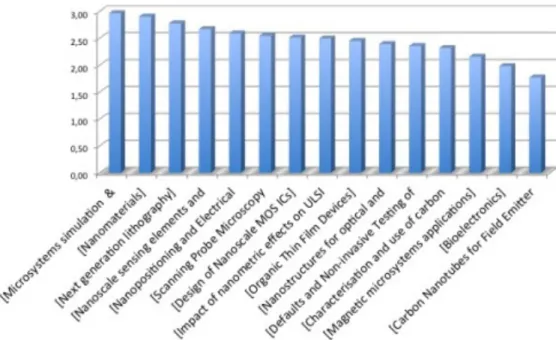
offered. We have first established a list of courses according to the miscellaneous competences available in the various universities involved in the project. The courses have been selected to cover as many topics as possible in relationship with nanoelectronics. Fifteen different courses have been proposed:
Bioelectronics, Carbon nanotubes for field emitter applications, Characterization and use of carbon nanotubes, Defaults and non-invasive testing of nanodevices, Design of nanoscale MOS integrated circuits (ICs), Impact of nano-metric effects on ultra large scale integration (ULSI) system performances, Magnetic
microsystems applications, Microsystems simulation and characterization,
Nanomaterials, Nano-positioning and electrical nano-probes for nanoelectronics, Nanoscale sensing elements and device production, Nano-structures for optical and magnetic applications, Next generation lithography, Organic thin film devices, and Scanning probe microscopy applications for nanoelectronics.
In order to define the priorities, it was important to collect not only the feedback of each expert answering the survey but also to have an idea of the number of persons involved. By the way, a manager may answer for all his related team. Thanks to SITELESC, the French professional organisation in microelectronics, which is a partner of the project, the survey has been submitted to many
representatives of the microelectronic companies including the largest in the area, such as ST Microelectronics, NXP (Philips), E2V, ATME, and Infineon
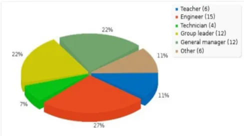
(Siemens). We have collected 85 answers. If we consider that managers leading large teams have provided most of the answers, the analysis should cover the needs of about 14,500 persons. The chart (Figure 1) shows the repartition of the responsibility level of the persons who answered the survey.
Figure 1. Users’ profiled in the survey.
It is important to notice that about 40% of the persons who answered the survey are group leaders or general managers. Repartition of others is almost
homogeneous between technicians, engineers and teachers. We can conclude that the results from this survey are very representative of the real global needs. After a detailed analysis of the needs (Figure 2) both, in term of interest and in term of potential trainees, a selection has been made among the proposed topics.
Figure 2. Topics of courses responding to the user from industry needs analysis. Curriculum Design Approach
Engineering education involves the use and application of skills for finding solutions, making decisions, and thinking effectively, i.e., problem-solving skills (Tzanova, 2005). So, instructional strategies and tactics for higher-level skills (Tzanova et al., 2010) were used in the course design. In this project discovery inductive strategy is implemented (when it is possible from a pedagogical point of view) in an interactive web-based instruction (related most to problem-solving). Specific tasks are designed for competences training (Martínez-Mediano, 2010), e.g., group work and tasks to manage a team or plan a new work organisation for implementation of new technology.
The web-based learning materials of ten courses are developed and professional videos of some lectures and of the practical work in the clean rooms and
laboratories. The videos are made by the experts from Tel Aviv University. Live Webcasts of an event, with an interactive talkback facility, can further enhance the quality of the experience. Such a portal was built by Tel Aviv University for Nano2Life (http://n2lvip.tau.ac.il) and maintained during the whole life cycle of the project. The site contains around 300 lectures on Nano bio topics.
Quality assurance (QA) is an integral part of the internal management of all partner institutions following the standards in the European Higher Education Area and the new courses are objects of these QA procedures.
So, the universities share their infrastructure, technological and human resources; they recognise the courses/credits, but each university keeps its autonomy for the national diploma delivery. To facilitate the implementation of the results during the project lifetime, the new courses are added to the list of electives to avoid complicated procedures of a whole curriculum change in each country. The expected added value for the students is in the highest quality of the
specialised courses developed by the best departments in the field, the opportunity to study more courses from the home institution and most importantly – the opportunity to learn practical skills and competences in the laboratories with advanced equipment and facilities.
Work in Progress
Because of the differences in the national regulations in each country, we considered that at this stage planning accreditation of joint or multiple MSc degrees for the next two years was not realistic. The courses were designed for specific learning outcomes, with credits for each course unit to be given after assessment, and adopted by all partner institutions. These credits will be transferred to the MSc programme in nanoelectronics at the partner university where the student is enrolled. ECTS credits are fully recognised, but the grades according to the norms of the country are still required. Therefore, a system for transfer of local grades in the five countries is set.
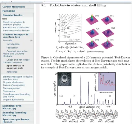
Some examples of the course modules under development are provided in Figure 3 and Figure 4.
Figure 3. Example of the “Atomic Force Microscope” module.
Figure 4. Example of the module “Spin effect in quantum dots.”
The project is in its third year, in the implementation stage. Each course was designed by the best laboratory/ department in the field with the necessary infrastructure and facilities for practical work. Students are now working on the Web-based materials, mostly theoretical with some assignments taken from the real practice at the workplace. After successfully passing the test of the e-learning course, the students will perform the practice in the partners’ laboratories,
followed by practical assessment. The mobility will be no more than a week of practice starting in June 2013.
The practical modules assessments are with practical tests, and they depend on the results of the tasks to be performed in the laboratory/clean room. After successful assessment, the student will obtain a certificate with the corresponding credits and the local grade of the host institution system with corresponding grade of the student's home institution system. Questionnaires and interviews will be used to measure the students and teachers attitudes, satisfaction, to reveal problems if any and to improve the courses and the collaborative MSc degree courses delivery.
Evaluation and Exploitation
The purpose of the evaluation within the project is to serve decision-making but its main goal is to help core developers and the new users in the improvement of
the product and development process. It is more oriented to the end users, e.g., to obtain feedback to help developers to improve the products and services as well as to optimise the development process trough early diagnosis of defects, to reveal unforeseen circumstances in the learning environment, to insure better
communication in the development team, to measure whether training objectives and trainees’ needs have been achieved and determine whether results could be used for decisions about the implementation and dissemination of the products and for new training modules development.
Expert reviews and design walkthrough in the early stages of materials design and prototypes production provided information and corresponding feedback to developers for ensuring the quality of content and usability aspects of prototypes, and to validate the efficiency of chosen methods and media as early as possible. To meet the users’ needs a prototyping approach was used in the environment and course adaptation/upgrade and a large audience will be involved in the pilot tests. The representatives of the decision-makers are being invited to all project
meetings and in the pilot test. Trainees were involved in the evaluation process when the first versions of prototypes were ready. Interviews and questionnaires to gather data on learners’ attitudes and opinions will be used.
Quality assessment is based on a careful procedure of self-evaluation by the institutions involved in the project, followed by external evaluation by peers. The external peers test whether the self-evaluation has been done carefully. They will report their own conclusions and recommendations.
After the pilot test and the final improvement of the environment and the courses, they will be incorporated in the regular training practices of the partner institution from universities and hospitals. To be used in the day-to-day practice in these institutions, the courses will be updated every 6 months correspondingly to the rate of technology development.
Expected Impact
We expect an impact of this curriculum development project on:
• The approach: In sharing facilities and expertise of four European universities in the new science of nanoetechnology, universities will provide the best education for the new jobs in the sector.
• The target groups: The contribution for the students will be in the highest quality of the specialised courses developed by the best departments in the field, the opportunity to study more courses from the home institution and most importantly – the opportunity to learn practical skills and
competences in the laboratories with advanced equipment and facilities; • The educational system: Each university will be “keeping” its MSc
students, and at the same time the students and the teachers will profit from the collaborative curriculum. University engineering education will improve through innovation of educational curricula with the newest
scientific and technological content and clearer relationship between learning processes in the university and at the real workplace.
Summary and Conclusions
In this manuscript we presented a work in progress within the European Community project “Master Degree Modules in Nanotechnologies for Electronics.” The project is aimed at common MSc degree level course
development for the new skills needed for the new jobs in the multidisciplinary nanoelectronics and a new job organisation.
In this project we adapted the approach of the big enterprises in the sector to share the research and development facilities and expertise despite the competition (or just to be competitive). The innovative solutions provided are:
• Sharing of resources, which a single university can not afford, for improving the education in high technologies for the new jobs in nano- bionano-technology in the LLP countries,
• Enriching the collaboration in sharing resources with – Israel and Switzerland.
• Virtual mobility. In this project the mobility is mostly virtual thanks to the e-learning courses, and only for the practical modules the short student mobility of one week is necessary.
Acknowledgments
This work has been financially supported by the Erasmus Program of the EACEA, project NanoEl, grant number, 510196-LLP-1-2010-1-IT-ERASMUS-ECDCE.
References
Eurofound, (2008). The future of the European biomedical healthcare sector: Four scenarios. Dublin, Ireland: European Monitoring Centre on Change. Retrieved from http://www.eurofound.europa.eu/pubdocs/
2007/1116/en/1/ef071116en.pdf
Investing in the Future of Jobs and Skills Scenarios, implications and options in anticipation of future skills and knowledge needs, DG EMPL projects VC/2007/0866 (2009). Comprehensive sectoral analysis of emerging competences and economic activities in the European Union (Lot 7, sector report, computer, electronic and optical products). Retrieved from
http://ec.europa.eu/employment_social/progress/index_en.html.
Martínez-Mediano, C., Castro, M., Mileva, N., Stoyanov, S., Kicken, W., Díaz, G., Riopérez, N., …. Martín, S. (2010, April). Internet-based performance-centered learning environment for curriculum support and its application in mlearning. Proceedings of The Future of Global Learning in Engineering Education Conference (pp. 819-824), 14-16 April, Madrid, Spain.
Morey-Chaisemartin P., Tzanova S., Schintke S., Demarchi, D., Barokas, J. (2012). Industry needs analysis for developing new skills in nano-electronics, Proceedings European Workshop on Microelectronics Education (EWME). Grenoble, France. Retrieved from
http://www.eda-publishing.org/Proceedings/EWME_proceedings2012BD.pdf
New Skills for New Jobs, matching labour market and skills needs (2008). Communication from the Commission to the European Parliament, the
Council, the European Economic and Social Committee and the Committee of the Regions,{COM (2008) 868 final}. Retrieved from
http://eur-lex.europa.eu/LexUriServ/LexUriServ.do?uri=COM:2008:0868:FIN:EN:PDF Tzanova S. (2005). An European Project for Internet-based Performance Centred
Instruction in Microelectronics. Proceedings: Ed- Media 2005 World
Conference on Educational Multimedia, Hypermedia & Telecommunications, Montréal, 2005 (pp. 215-218). June 27 – July 2, 2005. Montreal, Canada. Tzanova S., Codreanu N. (2010). Training Microsystems Technologies in an European eLearning Environment. Proceedings of The Future of Global Learning in Engineering Education Conference (pp. 113-118), 14-16 April, Madrid, Spain. Author Details Slavka Tzanova, [email protected] Danilo Demarchi [email protected] Philippe Morey-Chaisemartin [email protected]