Analysis of Capacitive Fed Microstrip Antenna for
Wideband Applications
Sandeep Kumar, Manish Rai, Dr. Jayanta Ghosh
Abstract – The parametric analysis of capacitive fed microstrip antenna suspended above the ground plane has been presented in this paper. For the analysis purpose, the reference structure has been taken from paper [3]. In this paper parameters of capacitive fed microstrip antenna is varied and the corresponding variation of radiation performance (return loss, bandwidth) is analyzed using IE3D software. A comparative plot of variation of return loss with frequency for capacitive coupled rectangular microstrip antenna is observed for each parameter.
Keywords – Microstrip Antenna, Capacitive Coupled, Bandwidth.
I. I
NTRODUCTIONMicrostrip antennas are suitable for modern broadband applications because of their desirable characteristics [1]–
[2]. Although microstrip antennas in their basic form exhibit limited bandwidth, it has been shown by several researchers that the bandwidth can be significantly improved by altering the basic geometry and/or feed or by using impedance matching techniques [1].
In this paper we have selected a capacitive fed microstrip antenna suspended above the ground plane from the paper [3]. The structure has utilized the capacitive feeding along with the introduction of air gap in between the ground plane for bandwidth enhancement. Thus this structure can be utilized for wideband applications. The parametric study of the structure has been done by varying each and every parameter of the patch structure. The further details are given in following sections.
II. T
HEORETICALC
ONSIDERATIONFig. 1 shows the geometrical configuration of the proposed antenna. Where the larger patch works as the radiator and the smaller patch serves as a feed strip which couples the energy to the radiator by electromagnetic coupling.
(a)
(b)
Fig.1(a). Top view of patch (b) 3D view of patch
A. Theoretical analysis of Rectangular patch
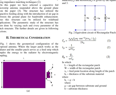
The equivalent circuit of the rectangular patch is represented as a parallel combination of resistor, inductor and capacitor with probe inductance is shown in fig. 2. The corresponding values of the Capacitor(Cp), Inductor(Lp) and Resistor(Rp) is given by the equation 1,2 and 3.
Fig. 2 Equivalent circuit of Rectangular Patch
In which
L = length of the rectangular patch W = width of the rectangular patch
xo= feed point location along length of the patch he= thickness of the substrate material
where he = g + h where
The effective dielectric constant of the substrate is given as
The input impedance of the patch is given below
Theoretical analysis of gap
The gap between the patches can be represented by π -circuit. The Cg, Cp1, and Cp2are the gap coupling and plate capacitances respectively, that can calculated from[4].
Fig.3.Equivalent π-circuit for gap
Fig. 4 Equivalent circuit of the patch
III. P
ARAMETRICA
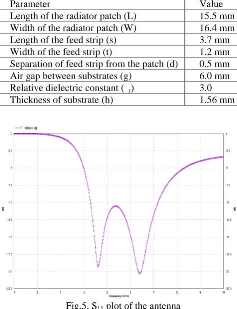
NALYSISFor the parametric analysis the dimension of the reference patch structure is given in the table below. The S11(input reflection coefficient) plot for the given patch is drawn by the simulation using IE3D software
Table 1 Dimension for the antenna designed for 5.9 GHz
Parameter Value
Length of the radiator patch (L) 15.5 mm Width of the radiator patch (W) 16.4 mm
Length of the feed strip (s) 3.7 mm
Width of the feed strip (t) 1.2 mm
Separation of feed strip from the patch (d) 0.5 mm Air gap between substrates (g) 6.0 mm Relative dielectric constant(εr) 3.0
Thickness of substrate (h) 1.56 mm
Fig.5. S11plot of the antenna
The bandwidth for the above dimension is observed to be 2.9 GHz with the centre frequency 5.9 GHz. Thus the overall percentage bandwidth is observed to be around 50%. The return loss upto -20 db has been observed at two resonating frequencies
B. Observation Table
Now each parameters of the antenna is varied keeping the other parameters constant and the corresponding variation of the antenna characteristics is tabulated below.
Bandwidth(B.W.), Resonating Frequency(Fc1, Fc2) are in GHz and the return loss(RL1 ,RL2) are in dB.
Table 2. Variation of Length of the patch
Length(mm) B.W. Fc1 RL1 Fc2 RL2
13.5 2.7 4.9 -15 6.7 -12.5
14.5 2.8 4.8 -17 6.5 -15.9
16.5 2.9 4.5 -22.5 6.3 -28.5
17.5 2.9 4.4 -27 6.2 -34
Table 3. Variation of Width of the patch
Width(mm) B.W. Fc1 RL1 Fc2 RL2
14.4 3 4.6 -18.5 6.5 -22
15.4 2.9 4.6 -18.5 6.5 -21
17.4 2.8 4.6 -19.8 6.4 -19.8
18.4 2.7 4.6 -20 6.2 -19
Table 4. Variation of Height of the patch
Height(mm) B.W. Fc1 RL1 Fc2 RL2
0.5 3.3 5.4 -30 7.5 -33
2 2.7 4.5 -17 6.1 -18.4
3 2.4 4 -14 5.5 14.2
Table 5. Variation of Dielectric Constant of substrate
εr B.W. Fc1 RL1 Fc2 RL2
2 3.1 5.2 -32 7 -20
4 2.6 4.2 -13.5 6 -22.5
5 1.4 4 -10.6 5.6 -25
6 1 3.8 -8.9 5.2 -31.4
Table 6. Variation of air gap of the substrate Air
gap(mm)
B.W. Fc1 RL1 Fc2 RL2
4 1.6 5.1 -28.5 7.1 -18
5 3 4.8 -22 6.7 -38.3
7 2.7 4.3 -17.3 6.1 -14.2
8 1 4.2 -16 5.8 -11
Table 7. Variation of distance between feed strip and patch
Width(t) (mm)
B.W. Fc1 RL1 Fc2 RL2
0.4 2.9 4.5 -17 6.4 -19
0.75 2.9 4.8 -27 6.4 -24
1 2.9 4.8 -48 6.5 -29
2 2.9 5 -17 6.6 -28
Table 8. Variation of Width of the feed strip Width(t)
(mm)
B.W. Fc1 RL1 Fc2 RL2
2 3.2 4.8 -24 6.8 -40
3 3 4.8 -28 6.5 -24
5 1.3 4.9 -13 6.2 -15.4
6 1 4.2 -10.5 6.1 -13
C. Simulated Comparative S11Plot
The results of the parameter variation tabulated above have been compared with the help of IE3D software. And a comparative plot of the parameter variation has been shown in fig below showing the corresponding radiation performance (bandwidth, centre frequency, return loss) of antenna
Fig.6. Plot for variation of length
Fig 7. Plot for variation of Width
Fig 8. Plot for variation of Height
Fig.10. Plot for variation in air gap
Fig.11. Plot for variation in distance between feed and patch
Fig.12. Plot for variation in width of feed
IV. R
ESULT ANDD
ISCUSSIONFrom the above tables and comparative S11 plots, we observe a certain relationship between the antenna characteristics (bandwidth, return loss, centre frequency) and the antenna parameters. By the help of this relationship the antenna characteristics can be adjusted for some particular requirement. On increasing the length of
loss with small decrease in centre frequency. We observe up to 63% variation in return loss by 22% increase in length of the radiating patch. On increasing the width, the bandwidth of antenna decreases without any variation in centre frequency. With decrease in height of the substrate, there is an increment in bandwidth as well as return loss, also the centre frequency (Fc) shifts left side. With reduction in the value of the dielectric constant, the bandwidth of antenna increases with increase in the centre frequency. The return loss also gets improved by 36% with an increase in dielectric constant. There is a slight variation of bandwidth with air gap. The centre frequency decreases with increase in air gap. By decreasing the width of the feed patch of the microstrip antenna up to 66%, there is an improvement of bandwidth up to 68%.
Thus from the above discussion we observe that for improving bandwidth of antenna we should have to decrease width, height of the radiating patch, dielectric constant of the substrate and the width of the feed patch. Again for decreasing the centre frequency we can increase the length, height of the radiating patch, dielectric constant of the substrate and the air gap
.
V. C
ONCLUSIONFrom the analysis it is concluded that the proposed antenna provides ultra wideband operation. The resonance frequencies are highly dependent on the air gap thickness, gap between patches and width of feed patch, these parameters play crucial role in controlling bandwidth as well as the antenna performance. Thus by modifying the antenna structure with the help of above results, it can be used for various wideband applications requiring different antenna performances.your manuscript electronically for review.
R
EFERENCES[1] R. Garg, P. Bhartia, I. Bahl, and A. Ittipiboon, Microstrip Antenna Design Handbook. Norwood, MA: Artech House, 2001. [2] C. A. Balanis, “Antenna Theory, Analysis and Design,” John
Wiley & Sons, New York, 1997.
[3] V. G. Kasabegoudar, D. S. Upadhyay, and K. J. Vinoy, “Design studies of ultra wideband microstrip antennas with a small capacitive feed,”Int. J. Antennas Propag., vol. 2007, pp. 1–8. [4] Veeresh G. Kasabegoudar and K. J. Vinoy,”Coplanar
capacitively coupled probe fed microstrip antennas for
Wideband applications”, IEEE transactions on antennas and propagation, vol. 58, no. 10, October 2010.
[5] K. Bhattacharjee, S. R. B. Chaudhuri, A. Mukherjee, D. R. Poddar, and S. K. Chowdhury, “Input impedance of rectangular microstrip antennas,”Proc. Inst. Elect. Eng. Pt. H., vol. 135, no. 5, pp. 351–352, 1988.
[6] F. Abboud, J. P. Damiano, and A. Papiernik, “Simple model for the input impedance of the coax-feed rectangular microstrip patch antenna for CAD,”Proc. Inst. Elect. Eng., vol. 135, no. 5, pp. 323–326, 1988.
A
UTHOR’
SP
ROFILESandeep Kumar
is currently pursuing M.Tech. from NIT Patna, India He has done his bachelor of engineering in electronics and communication stream. He is working on wideband microstrip antenna design.
Manish Rai
is currently pursuing M.Tech. from NIT Patna, India. He has done his Bachelor of Technology in Electronics and Communication stream. He is working on multifrequency microstrip antenna design.