NAVSTAR GLOBAL POSITIONING SYSTEM
INTERFACE SPECIFICATION
IS-GPS-200
Revision D
IRN-200D-001
7 March 2006
Navstar GPS Space Segment/Navigation User Interfaces
Deputy System Program Director
GPS JOINT PROGRAM OFFICE
Headquarters
Space and Missile Systems Center (SMC)
Navstar GPS Joint Program Office (SMC/GP)
2420 Vela Way, Suite 1866
El Segundo, CA 90245-4659
U.S.A.
By
ARINC Engineering Services, LLC 2250 E. Imperial Highway, Suite 450
REVISION RECORD
REV DESCRIPTION DOCUMENT
DATE
APPROVED
NC Initial Release 25 Jan 1983
A Incorporates 200NC-001, 200NC-002, and IRN-200NC-003
25 Sep 1984
B Incorporates IRN-200A-001A 30 Nov 1987
C Incorporates IRN-200B-001 thru IRN-200B-007 10 Oct 1993
C Re-formatted in Microsoft Word 6.0 in GEMS compatible format 10 Oct 1993 12 Jan 1996 C Changed distribution status to Public Release 25 Sep 1997 20 Oct 1997 D Incorporates IRN-200C-001 thru IRN-200C-005R1, change
ICD-GPS-200 to IS-ICD-GPS-200, introduce and specify the requirements of Improved Clock and Ephemeris (ICE) message for L2 C signal, and other additional updates
7 Dec 2004 23 Nov 2004
Page Revision Record
Pages Revision Pages Revision
i IRN-200D-001 ii D iii IRN-200D-001 iv D v IRN-200D-001 vi D vii - xi IRN-200D-001 xii - xiii D
xiv - xvi IRN-200D-001
1 – 5 D 6 IRN-200D-001 7 – 17 D 18 IRN-200D-001 19 – 56 D 56a – 56l IRN-200D-001 57 – 193 D
TABLE OF CONTENTS
1. SCOPE...1
1.1 Scope ...1
1.2 IS Approval and Changes...1
2. APPLICABLE DOCUMENTS...3 2.1 Government Documents ...3 2.2 Non-Government Documents...3 3. REQUIREMENTS ...5 3.1 Interface Definition ...5 3.2 Interface Identification ...5 3.2.1 Ranging Codes ...5 3.2.1.1 P-Code...6 3.2.1.2 Y-Code ...6 3.2.1.3 C/A-Code ...6
3.2.1.4 L2 CM-Code (IIR-M, IIF, and subsequent blocks) ...6
3.2.1.5 L2 CL-Code (IIR-M, IIF, and subsequent blocks) ...6
3.2.1.6 Non-Standard Codes ...11 3.2.2 NAV Data...11 3.2.3 L1/L2 Signal Structure ...12 3.3 Interface Criteria...14 3.3.1 Composite Signal ...14 3.3.1.1 Frequency Plan...14 3.3.1.2 Correlation Loss ...14
3.3.1.3 Carrier Phase Noise...14
3.3.1.4 Spurious Transmissions...14
3.3.1.5 Phase Quadrature...15
3.3.1.6 User-Received Signal Levels ...15
3.3.1.7 Equipment Group Delay...17
3.3.1.7.1 Group Delay Uncertainty ...17
3.3.1.7.2 Group Delay Differential ...17
3.3.1.8 Signal Coherence...17
3.3.1.9 Signal Polarization ...17
3.3.2 PRN Code Characteristics ...18
3.3.2.2 P-Code Generation ...20
3.3.2.3 C/A-Code Generation...30
3.3.2.4 L2 CM-/L2 CL-Code Generation...35
3.3.3 Navigation Data...38
3.3.3.1 Navigation Data Modulation (L2 CM)...38
3.3.3.1.1 Forward Error Correction...38
3.3.4 GPS Time and SV Z-Count...40
4. NOT APPLICABLE...43
5. NOT APPLICABLE...45
6. NOTES...47
6.1 Acronyms ...47
6.2 Definitions ...51
6.2.1 User Range Accuracy...51
6.2.2 SV Block Definitions ...51 6.2.2.1 Developmental SVs...51 6.2.2.2 Operational SVs ...51 6.2.2.2.1 Block II SVs...51 6.2.2.2.2 Block IIA SVs...51 6.2.2.2.3 Block IIR SVs ...52 6.2.2.2.4 Block IIR-M SVs ...52 6.2.2.2.5 Block IIF SVs...52
6.2.3 Operational Interval Definitions...52
6.2.3.1 Normal Operations ...52
6.2.3.2 Short-term Extended Operations ...52
6.2.3.3 Long-term Extended Operations ...52
6.2.4 GPS Week Number ...53
6.2.5 L5 Civil Signal ...53
6.3 Supporting Material...53
6.3.1 Received Signals ...53
6.3.2 Extended Navigation Mode (Block II/IIA)...55
6.3.3 Block IIA Mode (Block IIR/IIR-M)...56
6.3.4 Autonomous Navigation Mode ...56
6.3.5 PRN Code sequences expansion ... 56a
6.3.5.1 Additional C/A-code PRN sequences ... 56a
6.3.5.2.1 Additional P-code Generation...56b
6.3.5.3 Additional L2 CM-/L2 CL-Code PRN sequences...56i
10. APPENDIX I. LETTERS OF EXCEPTION...57
10.1 Scope ...57
10.2 Applicable Documents ...57
10.3 Letters of Exception ...57
20. APPENDIX II. GPS NAVIGATION DATA STRUCTURE FOR DATA, D(t) ...65
20.1 Scope ...65 20.2 Applicable Documents. ...65 20.2.1 Government Documents...65 20.2.2 Non-Government Documents...65 20.3 Requirements...67 20.3.1 Data Characteristics...67 20.3.2 Message Structure ...67 20.3.3 Message Content ...81 20.3.3.1 Telemetry Word ...81
20.3.3.2 Handover Word (HOW)...81
20.3.3.3 Subframe 1 ...83
20.3.3.3.1 Subframe 1 Content...83
20.3.3.3.2 Subframe 1 Parameter Characteristics ...86
20.3.3.3.3 User Algorithms for Subframe 1 Data ...86
20.3.3.4 Subframes 2 and 3 ...93
20.3.3.4.1 Content of Subframes 2 and 3 ...93
20.3.3.4.2 Subframe 2 and 3 Parameter Characteristics...95
20.3.3.4.3 User Algorithm for Ephemeris Determination ...95
20.3.3.4.4 NMCT Validity Time...101
20.3.3.5 Subframes 4 and 5 ...102
20.3.3.5.1 Content of Subframes 4 and 5 ...102
20.3.3.5.2 Algorithms Related to Subframe 4 and 5 Data...117
20.3.4 Timing Relationships ...126
20.3.4.1 Paging and Cutovers...126
20.3.4.2 SV Time vs. GPS Time ...126
20.3.4.3 Speed of Light ...126
20.3.4.4 Data Sets...127
20.3.5 Data Frame Parity...133
20.3.5.1 SV/CS Parity Algorithm...133
20.3.5.2 User Parity Algorithm ...133
30. APPENDIX III. GPS NAVIGATION DATA STRUCTURE FOR CNAV DATA, DC(t)...137
30.1 Scope ...137 30.2 Applicable Documents. ...137 30.2.1 Government Documents...137 30.2.2 Non-Government Documents...137 30.3 Requirements...139 30.3.1 Data Characteristics...139 30.3.2 Message Structure ...139 30.3.3 Message Content ...139
30.3.3.1 Message Type 10 and 11 Ephemeris and Health Parameters ...155
30.3.3.1.1 Message Type 10 and 11 Ephemeris and Health Parameter Content ...155
30.3.3.1.2 Message Type 10 and 11 Ephemeris Parameter Characteristics ...158
30.3.3.1.3 User Algorithm for Determination of SV Position...158
30.3.3.2 Message Types 30 Through 37 SV Clock Correction Parameters. ...163
30.3.3.2.1 Message Type 30 Through 37 SV Clock Correction Parameter Content...163
30.3.3.2.2 Clock Parameter Characteristics ...163
30.3.3.2.3 User Algorithms for SV Clock Correction Data ...163
30.3.3.2.4 SV Clock Accuracy Estimates ...165
30.3.3.3 Message Type 30 Ionospheric and Group Delay Correction Parameters ...168
30.3.3.3.1 Message Type 30 Ionospheric and Group Delay Correction Parameter Content...168
30.3.3.4 Message Types 31, 12, and 37 Almanac Parameters...171
30.3.3.4.1 Almanac Reference Week...171
30.3.3.4.2 Almanac Reference Time...171
30.3.3.4.3 SV PRN Number...171
30.3.3.4.4 Signal Health (L1/L2/L5)...171
30.3.3.4.5 Midi Almanac Parameter Content...172
30.3.3.4.6 Reduced Almanac Parameter Content...172
30.3.3.5 Message Type 32 Earth Orientation Parameters (EOP) ...175
30.3.3.5.1 EOP Content ...175
30.3.3.6 Message Type 33 Coordinated Universal Time (UTC) Parameters ...179
30.3.3.6.1 UTC Parameter Content...179
30.3.3.7 Message Types 34, 13, and 14 Differential Correction Parameters ...181
30.3.3.7.1 Differential Correction Parameters Content...181
30.3.3.7.2 DC Data Packet...181
30.3.3.7.3 Application of Clock-Related DC Data...184
30.3.3.7.4 Application of Orbit-Related DC Data...184
30.3.3.7.5 SV Differential Range Accuracy Estimates ...186
30.3.3.8 Message Type 35 GPS/GNSS Time Offset...187
30.3.3.8.1 GPS/GNSS Time Offset Parameter Content ...187
30.3.3.8.2 GPS and GNSS Time ...187
30.3.3.9 Message Types 36 and 15 Text Messages...188
30.3.4 Timing Relationships ...189
30.3.4.1 Paging and Cutovers...189
30.3.4.2 SV Time vs. GPS Time ...190
30.3.4.3 Speed of Light ...190
30.3.5 Data Frame Parity...191
LIST OF FIGURES
Figure 3-1. Generation of P-, C/A-Codes and Modulating Signals ...19
Figure 3-2. X1A Shift Register Generator Configuration...21
Figure 3-3. X1B Shift Register Generator Configuration...22
Figure 3-4. X2A Shift Register Generator Configuration...23
Figure 3-5. X2B Shift Register Generator Configuration...24
Figure 3-6. P-Code Generation...26
Figure 3-7. P-Code Signal Component Timing ...27
Figure 3-8. G1 Shift Register Generator Configuration ...31
Figure 3-9. G2 Shift Register Generator Configuration ...32
Figure 3-10. Example C/A-Code Generation ...33
Figure 3-11. C/A-Code Timing Relationships...34
Figure 3-12. L2 CM-/L2 CL-Code Timing Relationships...36
Figure 3-13. L2 CM/L2 CL Shift Register Generator Configuration ...37
Figure 3-14. Convolutional Encoder ...39
Figure 3-15. Convolutional Transmit/Decoding Timing Relationships...39
Figure 3-16. Time Line Relationship of HOW Message ...42
Figure 6-1. User Received Minimum Signal Level Variations (Example, Block II/IIA/IIR)...54
Figure 10-1. Letters of Exception. ...59
Figure 20-1. Data Format ...69
Figure 20-2. TLM and HOW Formats...82
Figure 20-3. Sample Application of Correction Parameters...92
Figure 20-4. Ionospheric Model ...123
Figure 20-5. Example Flow Chart for User Implementation of Parity Algorithm...135
Figure 30-1. Message Type 10 - Ephemeris 1 ...141
Figure 30-2. Message Type 11 - Ephemeris 2 ...142
Figure 30-3. Message Type 30 - Clock, IONO & Group Delay ...143
Figure 30-4. Message Type 31 - Clock & Reduced Almanac ...144
Figure 30-5. Message Type 32 - Clock & EOP ...145
Figure 30-6. Message Type 33 - Clock & UTC...146
Figure 30-7. Message Type 34 - Clock & Differential Correction ...147
Figure 30-8. Message Type 35 - Clock & GGTO ...148
Figure 30-9. Message Type 36 - Clock & Text ...149
Figure 30-11. Message Type 12 - Reduced Almanac...151
Figure 30-12. Message Type 13 – Clock Differential Correction ...152
Figure 30-13. Message Type 14 – Ephemeris Differential Correction ...153
Figure 30-14. Message Type 15 - Text...154
Figure 30-15. Reduced Almanac Packet Content ...174
LIST OF TABLES
Table 3-I. Code Phase Assignments ...7
Table 3-II. Code Phase Assignments (IIR-M, IIF, and subsequent blocks only)...9
Table 3-III. Signal Configuration ...13
Table 3-IV. Composite L1 Transmitted Signal Phase ...16
Table 3-V. Received Minimum RF Signal Strength ...16
Table 3-VI. P-Code Reset Timing ...28
Table 3-VII. Final Code Vector States...29
Table 6-I Additional C/A-/P-Code Phase Assignments... 56c Table 6-II. Additional L2 CM-/L2 CL-Code Phase Assignments ...56i Table 20-I. Subframe 1 Parameters ...87
Table 20-II. Ephemeris Data Definitions ...94
Table 20-III. Ephemeris Parameters...96
Table 20-IV. Elements of Coordinate Systems ...97
Table 20-V. Data IDs and SV IDs in Subframes 4 and 5...105
Table 20-VI. Almanac Parameters ...107
Table 20-VII. NAV Data Health Indications ...109
Table 20-VIII. Codes for Health of SV Signal Components...110
Table 20-IX. UTC Parameters...113
Table 20-X. Ionospheric Parameters ...114
Table 20-XI. IODC Values and Data Set Lengths (Block II/IIA) ...128
Table 20-XII. IODC Values and Data Set Lengths (Block IIR/IIR-M/IIF) ...129
Table 20-XIII. Reference Times ...132
Table 20-XIV. Parity Encoding Equations...134
Table 30-I. Message Types 10 and 11 Parameters...159
Table 30-II. Elements of Coordinate System ...161
Table 30-III. Clock Correction and Accuracy Parameters ...164
Table 30-IV. Group Delay Differential Parameters...168
Table 30-V. Midi Almanac Parameters...173
Table 30-VI. Reduced Almanac Parameters...174
Table 30-VII. Earth Orientation Parameters ...176
Table 30-VIII. Application of EOP Parameters ...177
Table 30-IX. UTC Parameters...180
Table 30-XI. GPS/GNSS Time Offset Parameters...188 Table 30-XII. Message Broadcast Intervals...189
1. SCOPE
1.1 Scope. This Interface Specification (IS) defines the requirements related to the interface between the Space Segment (SS) of the Global Positioning System (GPS) and the navigation User Segment (US) of the GPS for radio frequency (RF) link 1 (L1) and link 2 (L2).
1.2 IS Approval and Changes. ARINC Engineering Services, LLC has been designated the Interface Control Contractor (ICC), and is responsible for the basic preparation, approval, distribution, retention, and Interface Control Working Group (ICWG) coordination of the IS in accordance with GP-03-001. The Navstar GPS Joint Program Office is the necessary authority to make this IS effective. The Joint Program Office (JPO) administers approvals under the auspices of the Configuration Control Board (CCB), which is governed by the appropriate JPO Operating Instruction (OI). Military organizations and contractors are represented at the CCB by their respective segment member. All civil organizations and public interest are represented by the Department of Transportation representative of the GPS JPO.
A proposal to change the approved version of this IS can be submitted by any ICWG participating organization to the GPS JPO and/or the ICC. The ICC is responsible for the preparation of the change paper and change coordination, in accordance with GP-03-001. The ICC prepares the change paper as a Proposed Interface Revision Notice (PIRN) and is responsible for coordination of PIRNs with the ICWG. The ICWG coordinated PIRN must be submitted to the GPS JPO CCB for review and approval.
The ICWG review period for all Proposed Interface Revisions Notices (PIRNs) is 45 days after receipt by individual addressees. A written request to extend the review period may be submitted to the ICC for consideration.
2. APPLICABLE DOCUMENTS
2.1 Government Documents. The following documents of the issue specified contribute to the definition of the interfaces between the GPS Space Segment and the GPS navigation User Segment, and form a part of this IS to the extent specified herein.
Specifications
Federal
None
Military
None
Other Government Activity
None Standards Federal None Military None Other Publications GP-03-001
14 Nov 2003 GPS Interface Control Working Group Charter
2.2 Non-Government Documents. The following documents of the issue specified contribute to the definition of the interfaces between the GPS Space Segment and the GPS Navigation User Segment and form a part of this IS to the extent specified herein.
Specifications None Other Publications
3. REQUIREMENTS
3.1 Interface Definition. The interface between the GPS Space Segment (SS) and the GPS navigation User Segment (US) includes two RF links, L1 and L2. Utilizing these links, the space vehicles (SVs) of the SS shall provide continuous earth coverage signals that provide to the US the ranging codes and the system data needed to accomplish the GPS navigation (NAV) mission. These signals shall be available to a suitably equipped user with RF visibility to an SV.
3.2 Interface Identification. The carriers of L1 and L2 are typically modulated by one or more bit trains, each of which normally is a composite generated by the modulo-2 addition of a pseudo-random noise (PRN) ranging code and the downlink system data (referred to as NAV data).
3.2.1 Ranging Codes. Three PRN ranging codes are transmitted: the precision (P) code which is the principal NAV ranging code; the Y-code, used in place of the P-code whenever the anti-spoofing (A-S) mode of operation is activated; and the coarse/acquisition (C/A) code which is used for acquisition of the P (or Y) code (denoted as P(Y)) and as a civil ranging signal. Code-division-multiple-access techniques allow differentiating between the SVs even though they may transmit at the same frequencies. The SVs will transmit intentionally "incorrect" versions of the C/A and the P(Y) codes where needed to protect the users from receiving and utilizing anomalous NAV signals as a result of a malfunction in the SV's reference frequency generation system. These two "incorrect" codes are termed non-standard C/A (NSC) and non-standard Y (NSY) codes.
For Block IIR-M, IIF, and subsequent blocks of SVs, two additional PRN ranging codes are transmitted. They are the L2 civil-moderate (L2 CM) code and the L2 civil-long (L2 CL) code. The SVs will transmit intentionally "incorrect" versions of the L2 CM and L2 CL codes where needed to protect the users from receiving and utilizing anomalous NAV signals as a result of a malfunction in the SV's reference frequency generation system. These "incorrect" codes are termed non-standard L2 CM (NSCM) and non-standard L2 CL (NSCL) codes. The SVs shall also be capable of initiating and terminating the broadcast of NSCM and/or NSCL code(s) independently of each other, in response to CS command.
3.2.1.1 P-Code. The PRN P-code for SV ID number i is a ranging code, Pi(t), of 7 days in length at a chipping
rate of 10.23 Mbps. The 7 day sequence is the modulo-2 sum of two sub-sequences referred to as X1 and X2i; their
lengths are 15,345,000 chips and 15,345,037 chips, respectively. The X2i sequence is an X2 sequence selectively
delayed by 1 to 37 chips thereby allowing the basic code generation technique to produce a set of 37 mutually exclusive P-code sequences of 7 days in length. Of these, 32 are designated for use by SVs and 5 are reserved for other purposes (e.g. ground transmitters, etc.). Assignment of these code phase segments by SV-ID number (or other use) is given in Table 3-I. Additional PRN P-code sequences with assigned PRN numbers are provided in Section 6.3.5.2, Table 6-I
3.2.1.2 Y-Code. The PRN Y-code is used in place of the P-code when the A-S mode of operation is activated. 3.2.1.3 C/A-Code. The PRN C/A-Code for SV ID number i is a Gold code, Gi(t), of 1 millisecond in length at a
chipping rate of 1023 Kbps. The Gi(t) sequence is a linear pattern generated by the modulo-2 addition of two
sub-sequences, G1 and G2i, each of which is a 1023 chip long linear pattern. The epochs of the Gold code are
synchronized with the X1 epochs of the P-code. As shown in Table 3-I, the G2i sequence is a G2 sequence
selectively delayed by pre-assigned number of chips, thereby generating a set of different C/A-codes. Assignment of these by GPS PRN signal number is given in Table 3-I. Additional PRN C/A-code sequences with assigned PRN numbers are provided in Section 6.3.5.1, Table 6-I
3.2.1.4 L2 CM-Code (IIR-M, IIF, and subsequent blocks). The PRN L2 CM-code for SV ID number i is a ranging code, CM,i(t), which is 20 milliseconds in length at a chipping rate of 511.5 Kbps. The epochs of the L2 CM-code
are synchronized with the X1 epochs of the P-code. The CM,i(t) sequence is a linear pattern which is short cycled
every count of 10230 chips by resetting with a specified initial state. Assignment of initial states by GPS PRN signal number is given in Table 3-II. Additional PRN L2 CM-code sequence pairs are provided in Section 6.3.5.3, Table 6-II
3.2.1.5 L2 CL-Code (IIR-M, IIF, and subsequent blocks). The PRN L2 CL-code for SV ID number i is a ranging code, CL,i(t), which is 1.5 seconds in length at a chipping rate of 511.5 Kbps. The epochs of the L2 CL-code are
synchronized with the X1 epochs of the P-code. The CL,i(t) sequence is a linear pattern which is generated using the
same code generator polynomial as the one used for CM,i(t). However, the CL,i(t) sequence is short cycled by
resetting with a specified initial state every code count of 767250 chips. Assignment of initial states by GPS PRN signal number is given in Table 3-II. Additional PRN L2 CL-code sequence pairs are provided in Section 6.3.5.3, Table 6-II
Table 3-I. Code Phase Assignments (sheet 1 of 2) Code Phase Selection Code Delay Chips
SV ID No. GPS PRN Signal No. C/A(G2 i)**** (X2i) C/A P First 10 Chips Octal* C/A First 12 Chips Octal P 1 2 3 4 5 6 7 8 9 10 11 12 13 14 15 16 17 18 19 1 2 3 4 5 6 7 8 9 10 11 12 13 14 15 16 17 18 19 2 ⊕ 6 3 ⊕ 7 4 ⊕ 8 5 ⊕ 9 1 ⊕ 9 2 ⊕ 10 1 ⊕ 8 2 ⊕ 9 3 ⊕ 10 2 ⊕ 3 3 ⊕ 4 5 ⊕ 6 6 ⊕ 7 7 ⊕ 8 8 ⊕ 9 9 ⊕ 10 1 ⊕ 4 2 ⊕ 5 3 ⊕ 6 1 2 3 4 5 6 7 8 9 10 11 12 13 14 15 16 17 18 19 5 6 7 8 17 18 139 140 141 251 252 254 255 256 257 258 469 470 471 1 2 3 4 5 6 7 8 9 10 11 12 13 14 15 16 17 18 19 1440 1620 1710 1744 1133 1455 1131 1454 1626 1504 1642 1750 1764 1772 1775 1776 1156 1467 1633 4444 4000 4222 4333 4377 4355 4344 4340 4342 4343 ⏐ ⏐ ⏐ ⏐ ⏐ ⏐ ⏐ ⏐ 4343 * In the octal notation for the first 10 chips of the C/A code as shown in this column, the first digit (1) represents a "1" for the first chip and the last three digits are the conventional octal representation of the remaining 9 chips. (For example, the first 10 chips of the C/A code for PRN Signal Assembly No. 1 are: 1100100000).
** C/A codes 34 and 37 are common.
*** PRN sequences 33 through 37 are reserved for other uses (e.g. ground transmitters).
**** The two-tap coder utilized here is only an example implementation that generates a limited set of valid C/A codes.
⊕ = "exclusive or"
NOTE: The code phase assignments constitute inseparable pairs, each consisting of a specific C/A and a specific P code phase, as shown above.
Table 3-I. Code Phase Assignments (sheet 2 of 2) Code Phase Selection Code Delay Chips
SV ID No. GPS PRN Signal No. C/A(G2i)**** (X2i) C/A P First 10 Chips Octal* C/A First 12 Chips Octal P 20 21 22 23 24 25 26 27 28 29 30 31 32 *** *** *** *** *** 20 21 22 23 24 25 26 27 28 29 30 31 32 33 34** 35 36 37** 4 ⊕ 7 5 ⊕ 8 6 ⊕ 9 1 ⊕ 3 4 ⊕ 6 5 ⊕ 7 6 ⊕ 8 7 ⊕ 9 8 ⊕ 10 1 ⊕ 6 2 ⊕ 7 3 ⊕ 8 4 ⊕ 9 5 ⊕ 10 4 ⊕ 10 1 ⊕ 7 2 ⊕ 8 4 ⊕ 10 20 21 22 23 24 25 26 27 28 29 30 31 32 33 34 35 36 37 472 473 474 509 512 513 514 515 516 859 860 861 862 863 950 947 948 950 20 21 22 23 24 25 26 27 28 29 30 31 32 33 34 35 36 37 1715 1746 1763 1063 1706 1743 1761 1770 1774 1127 1453 1625 1712 1745 1713 1134 1456 1713 4343 ⏐ ⏐ ⏐ ⏐ ⏐ ⏐ ⏐ ⏐ ⏐ ⏐ ⏐ ⏐ ⏐ ⏐ ⏐ ⏐ 4343 * In the octal notation for the first 10 chips of the C/A code as shown in this column, the first
digit (1) represents a "1" for the first chip and the last three digits are the conventional octal representation of the remaining 9 chips. (For example, the first 10 chips of the C/A code for PRN Signal Assembly No. 1 are: 1100100000).
** C/A codes 34 and 37 are common.
*** PRN sequences 33 through 37 are reserved for other uses (e.g. ground transmitters). **** The two-tap coder utilized here is only an example implementation that generates a limited
set of valid C/A codes.
⊕ = "exclusive or"
NOTE: The code phase assignments constitute inseparable pairs, each consisting of a specific C/A and a specific P code phase, as shown above.
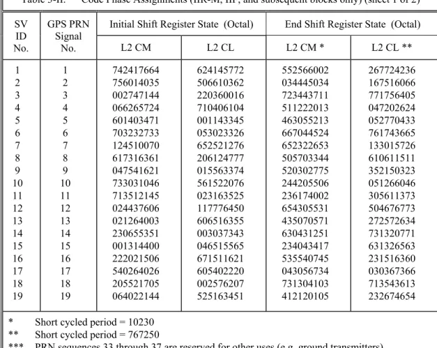
Table 3-II. Code Phase Assignments (IIR-M, IIF, and subsequent blocks only) (sheet 1 of 2) Initial Shift Register State (Octal) End Shift Register State (Octal) SV ID No. GPS PRN Signal No. L2 CM L2 CL L2 CM * L2 CL ** 1 2 3 4 5 6 7 8 9 10 11 12 13 14 15 16 17 18 19 1 2 3 4 5 6 7 8 9 10 11 12 13 14 15 16 17 18 19 742417664 756014035 002747144 066265724 601403471 703232733 124510070 617316361 047541621 733031046 713512145 024437606 021264003 230655351 001314400 222021506 540264026 205521705 064022144 624145772 506610362 220360016 710406104 001143345 053023326 652521276 206124777 015563374 561522076 023163525 117776450 606516355 003037343 046515565 671511621 605402220 002576207 525163451 552566002 034445034 723443711 511222013 463055213 667044524 652322653 505703344 520302775 244205506 236174002 654305531 435070571 630431251 234043417 535540745 043056734 731304103 412120105 267724236 167516066 771756405 047202624 052770433 761743665 133015726 610611511 352150323 051266046 305611373 504676773 272572634 731320771 631326563 231516360 030367366 713543613 232674654 * Short cycled period = 10230
** Short cycled period = 767250
*** PRN sequences 33 through 37 are reserved for other uses (e.g. ground transmitters). NOTE: There are many other available initial register states which can be used for other signal transmitters including any additional SVs in future.
Table 3-II. Code Phase Assignments (IIR-M, IIF, and subsequent blocks only) (sheet 2 of 2) Initial Shift Register State (Octal) End Shift Register State (Octal) SV ID No. GPS PRN Signal No. L2 CM L2 CL L2 CM * L2 CL ** 20 21 22 23 24 25 26 27 28 29 30 31 32 *** *** *** *** *** 20 21 22 23 24 25 26 27 28 29 30 31 32 33 34 35 36 37 120161274 044023533 724744327 045743577 741201660 700274134 010247261 713433445 737324162 311627434 710452007 722462133 050172213 500653703 755077436 136717361 756675453 435506112 266527765 006760703 501474556 743747443 615534726 763621420 720727474 700521043 222567263 132765304 746332245 102300466 255231716 437661701 717047302 222614207 561123307 240713073 365636111 143324657 110766462 602405203 177735650 630177560 653467107 406576630 221777100 773266673 100010710 431037132 624127475 154624012 275636742 644341556 514260662 133501670 641733155 730125345 000316074 171313614 001523662 023457250 330733254 625055726 476524061 602066031 012412526 705144501 615373171 041637664 100107264 634251723 257012032 703702423 * Short cycled period = 10230
** Short cycled period = 767250
*** PRN sequences 33 through 37 are reserved for other uses (e.g. ground transmitters). NOTE: There are many other available initial register states which can be used for other signal transmitters including any additional SVs in future.
3.2.1.6 Non-Standard Codes. The NSC, NSCM, NSCL, and NSY codes, used to protect the user from a malfunction in the SV's reference frequency system (reference paragraph 3.2.1), are not for utilization by the user and, therefore, are not defined in this document.
3.2.2 NAV Data. The NAV data, D(t), includes SV ephemerides, system time, SV clock behavior data, status messages and C/A to P (or Y) code handover information, etc. The 50 bps data is modulo-2 added to the P(Y)- and C/A- codes; the resultant bit-trains are used to modulate the L1 and L2 carriers. For a given SV, the data train D(t), if present, is common to the P(Y)- and C/A- codes on both the L1 and L2 channels. The content and characteristics of the NAV data, D(t), are given in Appendix II of this document.
For Block IIR-M, Block IIF, and subsequent blocks of SVs, civil navigation (CNAV) data, DC(t), also includes SV
ephemerides, system time, SV clock behavior, status messages, etc. The DC(t) is a 25 bps data stream which is
coded by a rate ½ convolutional coder. When selected by ground command, the resulting 50 sps symbol stream is modulo-2 added to the L2 CM-code; the resultant bit-train is combined with L2 CL-code using chip by chip time-division multiplexing method (i.e. alternating between L2 CM ⊕ data and L2 CL chips); the multiplexed bit-train is used to modulate the L2 carrier. The content and characteristics of the CNAV data, DC(t), are given in Appendix III
of this document.
During the initial period of Block IIR-M SVs operation, prior to Initial Operational Capability of L2 C signal, Block IIR-M may modulo-2 add the NAV data, D(t), to the L2 CM-code instead of CNAV data, DC(t). Moreover, the
NAV data, D(t), can be used in one of two different data rates which are selectable by ground command. D(t) with a data rate of 50 bps can be commanded to be modulo-2 added to the L2 CM-code, or D(t) with a symbol rate of 50 symbols per second (sps) (rate ½ convolutional encode of a 25 bps NAV data) can be commanded to be modulo-2 added to the L2 CM-code. The resultant bit-train is combined with L2 CL-code using chip by chip time-division multiplexing method (i.e. alternating between L2 CM ⊕ data and L2 CL chips). This multiplexed bit-train is used to modulate the L2 carrier.
3.2.3 L1/L2 Signal Structure. The L1 consists of two carrier components which are in phase quadrature with each other. Each carrier component is bi-phase shift key (BPSK) modulated by a separate bit train. One bit train is the modulo-2 sum of the P(Y)-code and NAV data, D(t), while the other is the modulo-2 sum of the C/A-code and the NAV data, D(t). For Block II/IIA and IIR, the L2 is BPSK modulated by only one of those two bit trains; the bit train to be used for L2 modulation is selected by ground command. A third modulation mode is also selectable on the L2 channel by ground command: it utilizes the P(Y)-code without the NAV data as the modulating signal. For a particular SV, all transmitted signal elements (carriers, codes and data) are coherently derived from the same on-board frequency source.
For Block IIR-M, Block IIF, and subsequent blocks of SVs, the L2 consists of two carrier components. One carrier component is BPSK modulated by the bit train which is the modulo-2 sum of the P(Y)-code with or without NAV data D(t), while the other is BPSK modulated by any one of three other bit trains which are selectable by ground command. The three possible bit trains are: (1) the modulo-2 sum of the C/A-code and D(t); (2) the C/A-code with no data and; (3) a chip-by-chip time multiplex combination of bit trains consisting of the L2 CM-code with DC(t)
and the L2 CL-code with no data. The L2 CM-code with the 50 sps symbol stream of DC(t) is time-multiplexed
with L2 CL-code at a 1023 kHz rate as described in paragraph 3.2.2. The first L2 CM-code chip starts synchronously with the end/start of week epoch.
During the initial period of Block IIR-M SVs operation, prior to Initial Operational Capability of L2 C signal, Block IIR-M may modulo-2 add the NAV data, D(t), to the L2 CM-code instead of CNAV data, DC(t). In such
configuration, the data rate of D(t) may be 50 bps (i.e. without convolution encoding) or it may be 25 bps. The D(t) of 25 bps shall be convolutionally encoded resulting in 50 sps.
Table 3-III. Signal Configuration
L1 L2** SV Blocks
In-Phase* Quadrature-Phase* In-Phase* Quadrature-Phase*
Block II/IIA/IIR P(Y) ⊕ D(t) C/A ⊕ D(t)
P(Y) ⊕ D(t) or P(Y) or C/A ⊕ D(t) Not Applicable
Block IIR-M*** P(Y) ⊕ D(t) C/A ⊕ D(t) P(Y)
⊕ D(t) or P(Y) L2 CM ⊕ D(t) with L2 CL or L2 CM ⊕ D′(t) with L2 CL or C/A ⊕ D(t) or C/A
Block IIR-M/IIF P(Y) ⊕ D(t) C/A ⊕ D(t) P(Y)
⊕ D(t) or P(Y) L2 CM ⊕ DC(t) with L2 CL or C/A ⊕ D(t) or C/A
Notes: 1) The configuration identified in this table reflects only the content of Section 3.2.3 and does not show all available codes/signals on L1/L2.
2) It should be noted that there are no flags or bits in the navigation message to directly indicate which signal option is broadcast for L2 Civil (L2 C) signal.
⊕ = “exclusive-or” (modulo-2 addition) D(t) = NAV data at 50 bps
D′(t) = NAV data at 25 bps with FEC encoding resulting in 50 sps DC(t) = CNAV data at 25 bps with FEC encoding resulting in 50 sps
* Terminology of “in-phase” and “quadrature-phase” is used only to identify the relative phase quadrature relationship of the carrier components (i.e. 90 degrees offset of each other).
** The two carrier components on L2 may not have the phase quadrature relationship. They may be broadcast on same phase (ref. Section 3.3.1.5).
*** Possible signal configuration for Block IIR-M only during the initial period of Block IIR-M SVs operation, prior to Initial Operational Capability of L2 C signal. See paragraph 3.2.2.
3.3 Interface Criteria. The criteria specified in the following define the requisite characteristics of the SS/US interface for the L1 and L2.
3.3.1 Composite Signal. The following criteria define the characteristics of the composite signals.
3.3.1.1 Frequency Plan. The signals shall be contained within two 20.46-MHz bands centered about L1 and L2. The carrier frequencies for the L1 and L2 signals shall be coherently derived from a common frequency source within the SV. The nominal frequency of this source -- as it appears to an observer on the ground -- is 10.23 MHz. The SV carrier frequency and clock rates -- as they would appear to an observer located in the SV -- are offset to compensate for relativistic effects. The clock rates are offset by ∆f/f = -4.4647E-10, equivalent to a change in the P-code chipping rate of 10.23 MHz offset by a ∆f = -4.5674E-3 Hz. This is equal to 10.22999999543 MHz. The nominal carrier frequencies (f0) shall be 1575.42 MHz, and 1227.6 MHz for L1 and L2, respectively.
3.3.1.2 Correlation Loss. Correlation loss is defined as the difference between the SV power received in a 20.46 MHz bandwidth and the signal power recovered in an ideal correlation receiver of the same bandwidth. On the L1 and L2 channels, the worst case correlation loss occurs when the carrier is modulated by the sum of the P(Y) code and the NAV data stream. For this case, the correlation loss apportionment shall be as follows:
1. SV modulation imperfections 0.6 dB
2. Ideal UE receiver waveform distortion 0.4 dB (due to 20.46 MHz filter)
3.3.1.3 Carrier Phase Noise. The phase noise spectral density of the unmodulated carrier shall be such that a phase locked loop of 10 Hz one-sided noise bandwidth shall be able to track the carrier to an accuracy of 0.1 radians rms. 3.3.1.4 Spurious Transmissions. In-band spurious transmissions shall be at least 40 dB below the unmodulated L1 and L2 carriers over the allocated 20.46 MHz channel bandwidth.
3.3.1.5 Phase Quadrature. The two L1 carrier components modulated by the two separate bit trains (C/A-code plus data and P(Y)-code plus data) shall be in phase quadrature (within ±100 milliradians) with the C/A signal carrier lagging the P signal by 90 degrees. Referring to the phase of the P carrier when Pi(t) equals zero as the "zero phase
angle", the P(Y)- and C/A-code generator output shall control the respective signal phases in the following manner: when Pi(t) equals one, a 180-degree phase reversal of the P-carrier occurs; when Gi(t) equals one, the C/A carrier
advances 90 degrees; when the Gi(t) equals zero, the C/A carrier shall be retarded 90 degrees (such that when Gi(t)
changes state, a 180-degree phase reversal of the C/A carrier occurs). The resultant nominal composite transmitted signal phases as a function of the binary state of only the two modulating signals are as shown in Table 3-IV. For Block IIR-M, IIF, and subsequent blocks of SVs, phase quadrature relationship between the two L2 carrier components can be the same as for the two L1 carrier components as described above. However, for the L2 case, the civil signal carrier component is modulated by any one of three (IIF) or four (IIR-M) different bit trains as described in paragraph 3.2.3. Moreover, the two L2 carrier components can be in same phase. The resultant composite transmitted signal phases will vary as a function of the binary state of the modulating signals as well as the signal power ratio and phase quadrature relationship. Beyond these considerations, additional carrier components in Block IIR-M, IIF, and subsequent blocks of SVs will result in composite transmitted signal phase relationships other than the nominal special case of Table 3-IV.
For Block IIF, the crosstalk between the C/A, when selected, and P(Y) signals shall not exceed –20 dB in the L1 and L2. The crosstalk is the relative power level of the undesired signal to the desired reference signal.
3.3.1.6 User-Received Signal Levels. The SV shall provide L1 and L2 navigation signal strength at end-of-life (EOL), worst-case, in order to meet the minimum levels specified in Table 3-V. The minimum received power is measured at the output of a 3 dBi linearly polarized user receiving antenna (located near ground) at worst normal
orientation, when the SV is above a 5-degree elevation angle. The received signal levels are observed within the in-band allocation defined in para. 3.3.1.1.
The Block IIF SV shall provide L1 and L2 signals with the following characteristic: the L1 off-axis power gain shall not decrease by more than 2 dB from the Edge-of-Earth (EOE) to nadir, nor more than 10 dB from EOE to 20 degrees off nadir, and no more than 18 dB from EOE to 23 degrees off nadir; the L2 off-axis power gain shall not decrease by more than 2 dB from EOE to nadir, and no more than 10 dB from EOE to 23 degrees off nadir; the power drop off between EOE and ±23 degrees shall be in a monotonically decreasing fashion.
Table 3-IV. Composite L1 Transmitted Signal Phase ** (Block II/IIA and IIR SVs Only) Code State Nominal Composite L1 Signal Phase* P C/A 0° -70.5° +109.5° 180° 0 1 0 1 0 0 1 1 * Relative to 0, 0 code state with positive angles leading and negative angles lagging.
** Based on the composite of two L1 carrier components with 3 dB difference in the power levels of the two.
Table 3-V. Received Minimum RF Signal Strength Signal SV Blocks Channel P(Y) C/A or L2 C L1 -161.5 dBW -158.5 dBW II/IIA/IIR L2 -164.5 dBW -164.5 dBW L1 -161.5 dBW -158.5 dBW IIR-M/IIF L2 -161.5 dBW -160.0 dBW or
3.3.1.7 Equipment Group Delay. Equipment group delay is defined as the delay between the signal radiated output of a specific SV (measured at the antenna phase center) and the output of that SV's on-board frequency source; the delay consists of a bias term and an uncertainty. The bias term is of no concern to the US since it is included in the clock correction parameters relayed in the NAV data, and is therefore accounted for by the user computations of system time (reference paragraphs 20.3.3.3.3.1, 30.3.3.2.3). The uncertainty (variation) of this delay as well as the group delay differential between the signals of L1 and L2 are defined in the following.
3.3.1.7.1 Group Delay Uncertainty. The effective uncertainty of the group delay shall not exceed 3.0 nanoseconds (two sigma).
3.3.1.7.2 Group Delay Differential. The group delay differential between the radiated L1 and L2 signals (i.e. L1 P(Y) and L2 P(Y), L1 P(Y) and L2 C) is specified as consisting of random plus bias components. The mean differential is defined as the bias component and will be either positive or negative. For a given navigation payload redundancy configuration, the absolute value of the mean differential delay shall not exceed 15.0 nanoseconds. The random variations about the mean shall not exceed 3.0 nanoseconds (two sigma). Corrections for the bias components of the group delay differential are provided to the US in the Nav message using parameters designated as TGD (reference paragraph 20.3.3.3.3.2) and Inter-Signal Correction (ISC) (reference paragraph 30.3.3.3.1.1).
3.3.1.8 Signal Coherence. All transmitted signals for a particular SV shall be coherently derived from the same on-board frequency standard; all digital signals shall be clocked in coincidence with the PRN transitions for the P-signal and occur at the P-P-signal transition speed. On the L1 channel the data transitions of the two modulating signals (i.e., that containing the P(Y)-code and that containing the C/A-code), L1 P(Y) and L1 C/A, shall be such that the average time difference between the transitions does not exceed 10 nanoseconds (two sigma).
3.3.1.9 Signal Polarization. The transmitted signal shall be right-hand circularly polarized (RHCP). For the angular range of ±14.3 degrees from boresight, L1 ellipticity shall be no worse than 1.2 dB for Block II/IIA and shall be no worse than 1.8 dB for Block IIR/IIR-M/IIF SVs. L2 ellipticity shall be no worse than 3.2 dB for Block II/IIA SVs and shall be no worse than 2.2 dB for Block IIR/IIR-M/IIF over the angular range of ±14.3 degrees from boresight.
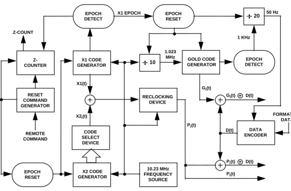
3.3.2 PRN Code Characteristics. The characteristics of the P-, L2 CM-, L2 CL-, and the C/A-codes are defined below in terms of their structure and the basic method used for generating them. Figure 3-1 depicts a simplified block diagram of the scheme for generating the 10.23 Mbps Pi(t) and the 1.023 Mbps Gi(t) patterns (referred to as P-
and C/A-codes respectively), and for modulo-2 summing these patterns with the NAV bit train, D(t), which is clocked at 50 bps. The resultant composite bit trains are then used to modulate the signal carriers.
3.3.2.1 Code Structure. The Pi(t) pattern (P-code) is generated by the modulo-2 summation of two PRN codes,
X1(t) and X2(t - iT), where T is the period of one P-code chip and equals (1.023 x 10⁷)-1 seconds, while i is an
integer from 1 through 37. This allows the generation of 37 unique P(t) code phases (identified in Table 3-I) using the same basic code generator.
The linear Gi(t) pattern (C/A-code) is the modulo-2 sum of two 1023-bit linear patterns, G1 and G2i. The latter
sequence is selectively delayed by an integer number of chips to produce many different G(t) patterns (defined in Table 3-I).
The CM,i(t) pattern (L2 CM-code) is a linear pattern which is reset with a specified initial state every code count of
10230 chips. Different initial states are used to generate different CM,i(t) patterns (defined in Table 3-II).
The CL,i(t) pattern (L2 CL-code) is also a linear pattern but with a longer reset period of 767250 chips. Different
initial states are used to generate different CL,i(t) patterns (defined in Table 3-II).
For a given SV-ID, two different initial states are used to generate different CL,i(t) and CM,i(t) patterns.
Section 6.3.5 provides a selected subset of additional P-, L2 CM-, L2 CL-, and the C/A-code sequences with assigned PRN numbers.
Figure 3-1. Generation of P-, C/A-Codes and Modulating Signals Z-COUNTER RESET COMMAND GENERATOR X1 CODE GENERATOR CODE SELECT DEVICE X2 CODE GENERATOR RECLOCKING DEVICE 10.23 MHz FREQUENCY SOURCE GOLD CODE GENERATOR EPOCH RESET EPOCH DETECT EPOCH RESET EPOCH DETECT 10 20 X1 EPOCH DATA ENCODER D(t) Pi(t) D(t) Pi(t) FORMATTED DATA Pi(t) X2i(t) X1(t) Gi(t) REMOTE COMMAND Z-COUNT 1.023 MHz 1 KHz 50 Hz Gi(t) D(t)
3.3.2.2 P-Code Generation. Each Pi(t) pattern is the modulo-2 sum of two extended patterns clocked at 10.23 Mbps
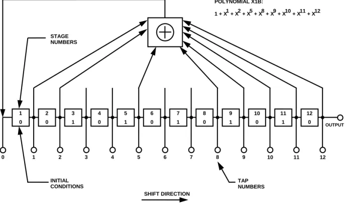
(X1 and X2i). X1 itself is generated by the modulo-2 sum of the output of two 12-stage registers (X1A and X1B)
short cycled to 4092 and 4093 chips respectively. When the X1A short cycles are counted to 3750, the X1 epoch is generated. The X1 epoch occurs every 1.5 seconds after 15,345,000 chips of the X1 pattern have been generated. The polynomials for X1A and X1B, as referenced to the shift register input, are:
X1A: 1 + X6 + X8 + X11 + X12, and
X1B: 1 + X1 + X2 + X5 + X8 + X9 + X10 + X11 + X12.
Samples of the relationship between shift register taps and the exponents of the corresponding polynomial, referenced to the shift register input, are as shown in Figures 3-2, 3-3, 3-4 and 3-5.
The state of each generator can be expressed as a code vector word which specifies the binary sequence constant of each register as follows: (a) the vector consists of the binary state of each stage of the register, (b) the stage 12 value appears at the left followed by the values of the remaining states in order of descending stage numbers, and (c) the shift direction is from lower to higher stage number with stage 12 providing the current output. This code vector convention represents the present output and 11 future outputs in sequence. Using this convention, at each X1 epoch, the X1A shift register is initialized to code vector 001001001000 and the X1B shift register is initialized to code vector 010101010100. The first chip of the X1A sequence and the first chip of the X1B sequence occur simultaneously in the first chip interval of any X1 period.
The natural 4095 chip cycles of these generating sequences are shortened to cause precession of the X1B sequence with respect to the X1A sequence during subsequent cycles of the X1A sequence in the X1 period. Re-initialization of the X1A shift register produces a 4092 chip sequence by omitting the last 3 chips (001) of the natural 4095 chip X1A sequence. Re-initialization of the X1B shift register produces a 4093 chip sequence by omitting the last 2 chips (01) of the natural 4095 chip X1B sequence. This results in the phase of the X1B sequence lagging by one chip for each X1A cycle in the X1 period.
The X1 period is defined as the 3750 X1A cycles (15,345,000 chips) which is not an integer number of X1B cycles. To accommodate this situation, the X1B shift register is held in the final state (chip 4093) of its 3749th cycle. It remains in this state until the X1A shift register completes its 3750th cycle (343 additional chips). The completion of the 3750th X1A cycle establishes the next X1 epoch which re-initializes both the X1A and X1B shift registers starting a new X1 cycle.
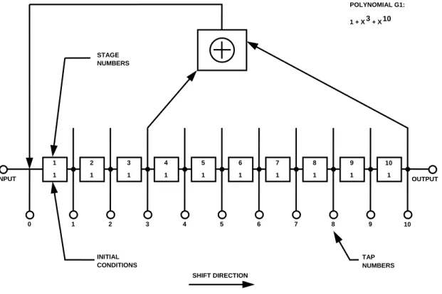
Figure 3-2. X1A Shift Register Generator Configuration 1 0 2 0 3 0 4 1 5 0 6 0 7 1 8 0 9 0 10 1 11 0 12 0 STAGE NUMBERS INITIAL CONDITIONS SHIFT DIRECTION 0 1 2 3 4 5 6 7 8 9 10 11 12 OUTPUT TAP NUMBERS POLYNOMIAL X1A: 1 + X6 + X8 + X11 + X12
Figure 3-3. X1B Shift Register Generator Configuration 1 0 2 0 3 1 4 0 5 1 6 0 7 1 8 0 9 1 10 0 11 1 12 0 STAGE NUMBERS INITIAL CONDITIONS SHIFT DIRECTION 0 1 2 3 4 5 6 7 8 9 10 11 12 OUTPUT TAP NUMBERS POLYNOMIAL X1B: 1 + X1 + X2 + X5 + X8 + X9 + X10 + X11 + X12
Figure 3-4. X2A Shift Register Generator Configuration 1 1 2 0 3 1 4 0 5 0 6 1 7 0 8 0 9 1 10 0 11 0 12 1 STAGE NUMBERS INITIAL CONDITIONS SHIFT DIRECTION 0 1 2 3 4 5 6 7 8 9 10 11 12 OUTPUT TAP NUMBERS POLYNOMIAL X2A: 1 + X1 + X3 + X4 + X5 + X7 + X8 + X9 + X10 + X11 + X12
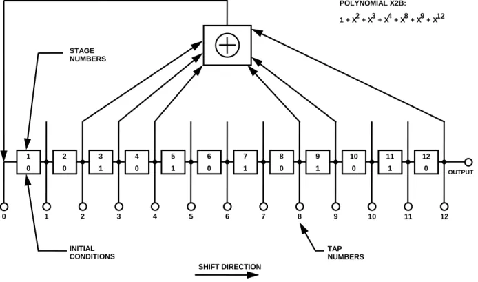
Figure 3-5. X2B Shift Register Generator Configuration 1 0 2 0 3 1 4 0 5 1 6 0 7 1 8 0 9 1 10 0 11 1 12 0 STAGE NUMBERS INITIAL CONDITIONS SHIFT DIRECTION 0 1 2 3 4 5 6 7 8 9 10 11 12 OUTPUT TAP NUMBERS POLYNOMIAL X2B: 1 + X2 + X3 + X4 + X8 + X9 + X12
The X2i sequences are generated by first producing an X2 sequence and then delaying it by a selected integer
number of chips, i, ranging from 1 to 37. Each of the X2i sequences is then modulo-2 added to the X1 sequence
thereby producing up to 37 unique P(t) sequences.
The X2A and X2B shift registers, used to generate X2, operate in a similar manner to the X1A and X1B shift registers. They are short-cycled, X2A to 4092 and X2B to 4093, so that they have the same relative precession rate as the X1 shift registers. X2A epochs are counted to include 3750 cycles and X2B is held in the last state at 3749 cycle until X2A completes its 3750th cycle. The polynomials for X2A and X2B, as referenced to the shift register input, are:
X2A: 1 + X1 + X3 + X4 + X5 + X7 + X8 + X9 + X10 + X11 + X12, and
X2B: 1 + X2 + X3 + X4 + X8 + X9 + X12.
(The initialization vector for X2A is 100100100101 and for X2B is 010101010100).
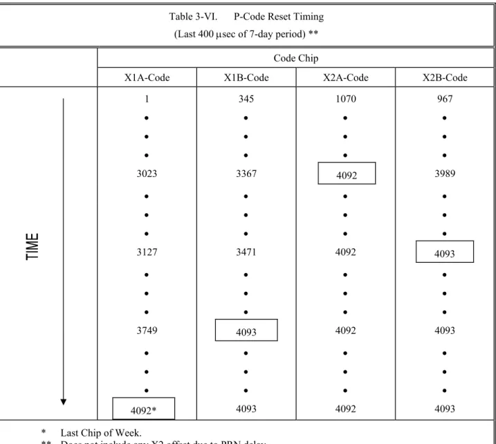
The X2A and X2B epochs are made to precess with respect to the X1A and X1B epochs by causing the X2 period to be 37 chips longer than the X1 period. When the X2A is in the last state of its 3750th cycle and X2B is in the last state of its 3749th cycle, their transitions to their respective initial states are delayed by 37 chip time durations. At the beginning of the GPS week, X1A, X1B, X2A and X2B shift registers are initialized to produce the first chip of the week. The precession of the shift registers with respect to X1A continues until the last X1A period of the GPS week interval. During this particular X1A period, X1B, X2A and X2B are held when reaching the last state of their respective cycles until that X1A cycle is completed (see Table 3-VI). At this point, all four shift registers are initialized and provide the first chip of the new week.
Figure 3-6 shows a functional P-code mechanization. Signal component timing is shown in Figure 3-7, while the end-of-week reset timing and the final code vector states are given in Tables 3-VI and 3-VII, respectively.
Figure 3-6. P-Code Generation X1A REGISTER C I 1 6 12 R 4093 DECODE 4092 DECODE 4092 DECODE 4093 DECODE C CLOCK CONTROL 3750 Z-COUNTER 403,200 X1B REGISTER C I 1 12 R X2A REGISTER C I 1 12 R X2B REGISTER C I 1 2 12 R 7 DAY RESET SHIFT REGISTER A 1, 2, 5, 8, 9, 10, 11, 12 1, 3, 4, 5, 7, 8, 9, 10, 11, 12 2, 3, 4, 8, 9, 12 6, 8, 11, 12 A CLOCK CONTROL B 3749 3750 37 C 3749 B CLOCK CONTROL 1 i 10.23 MHz C- CLOCK I - INPUT R- RESET TO INITIAL CONDITIONS ON NEXT CLOCK REGISTER INPUTS X1 EPOCH SET X1A EPOCH
RESUME HALT SET X1B EPOCH END/WEEK HALT START/WEEK ENABLE X2 EPOCH RESUME HALT END/WEEK SET X2B EPOCH X2 SET X2A EPOCH X1 X2i Pi
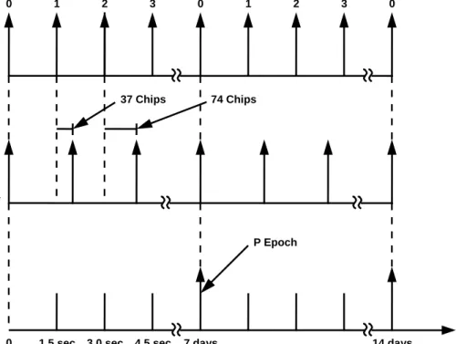
Figure 3-7. P-Code Signal Component Timing 0 1 2 3 0 1 2 3 0 X1 EPOCHS X2 EPOCHS * TIME 37 Chips 74 Chips P Epoch
0 1.5 sec 3.0 sec 4.5 sec 7 days 14 days
Table 3-VI. P-Code Reset Timing (Last 400 µsec of 7-day period) **
Code Chip
X1A-Code X1B-Code X2A-Code X2B-Code
1 345 1070 967 • • • • • • • • • • • • 3023 3367 4092 3989 • • • • • • • • • • • • 3127 3471 4092 4093 • • • • • • • • • • • • 3749 4093 4092 4093 • • • • • • • • • • • • 4092* 4093 4092 4093
* Last Chip of Week.
Table 3-VII. Final Code Vector States
Code Chip Number Vector State Vector State for 1st Chip following Epoch 4091 100010010010 X1A 4092 000100100100 001001001000 4092 100101010101 X1B 4093 001010101010 010101010100 4091 111001001001 X2A 4092 110010010010 100100100101 4092 000101010101 X2B 4093 001010101010 010101010100
3.3.2.3 C/A-Code Generation. Each Gi(t) sequence is a 1023-bit Gold-code which is itself the modulo-2 sum of two
1023-bit linear patterns, G1 and G2i. The G2i sequence is formed by effectively delaying the G2 sequence by an
integer number of chips. The G1 and G2 sequences are generated by 10-stage shift registers having the following polynomials as referred to in the shift register input (see Figures 3-8 and 3-9).
G1 = X10 + X3 + 1, and
G2 = X10 + X9 + X8 + X6 + X3 + X2 + 1.
The initialization vector for the G1 and G2 sequences is 1111111111. The G1 and G2 shift registers are initialized at the P-coder X1 epoch. The G1 and G2 registers are clocked at 1.023 MHz derived from the 10.23 MHz P-coder clock. The initialization by the X1 epoch phases the 1.023 MHz clock to insure that the first chip of the C/A code begins at the same time as the first chip of the P-code.
The effective delay of the G2 sequence to form the G2i sequence may be accomplished by combining the output of
two stages of the G2 shift register by modulo-2 addition (see Figure 3-10). However, this two-tap coder implementation generates only a limited set of valid C/A codes. Table 3-I contains a tabulation of the G2 shift register taps selected and their corresponding P-code X2i and PRN signal numbers together with the first several
Figure 3-8. G1 Shift Register Generator Configuration 1 1 2 1 3 1 4 1 5 1 6 1 7 1 8 1 9 1 10 1 STAGE NUMBERS INITIAL CONDITIONS SHIFT DIRECTION 0 1 2 3 4 5 6 7 8 9 10 OUTPUT TAP NUMBERS POLYNOMIAL G1: 1 + X3 + X10 INPUT
Figure 3-9. G2 Shift Register Generator Configuration 1 1 2 1 3 1 4 1 5 1 6 1 7 1 8 1 9 1 10 1 STAGE NUMBERS INITIAL CONDITIONS SHIFT DIRECTION 0 1 2 3 4 5 6 7 8 9 10 OUTPUT TAP NUMBERS POLYNOMIAL G2: 1 + X2 + X3 +X6 + X8 + X9 + X10 INPUT
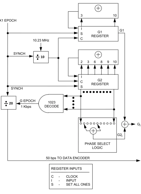
Figure 3-10. Example C/A-Code Generation 10 S C I C S I G1 REGISTER 2 3 6 8 9 10 G2 REGISTER 3 10 10.23 MHz SYNCH X1 EPOCH 20 SYNCH G EPOCH 1 Kbps 1023 DECODE 50 bps TO DATA ENCODER PHASE SELECT LOGIC G2i G1 REGISTER INPUTS C - CLOCK I - INPUT
S - SET ALL ONES
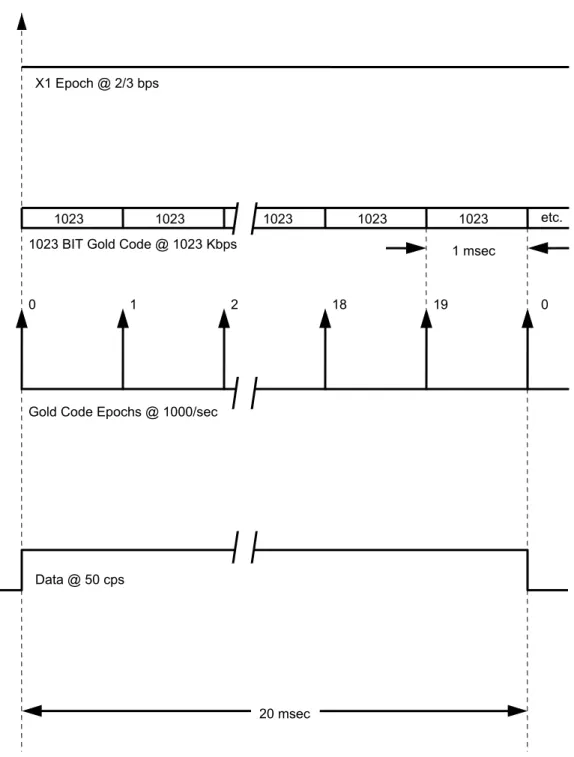
Figure 3-11. C/A-Code Timing Relationships
1023 etc.
X1 Epoch @ 2/3 bps
0 1 2 18 19 0
1 msec 1023 BIT Gold Code @ 1023 Kbps
1023 1023 1023 1023
Gold Code Epochs @ 1000/sec
Data @ 50 cps
3.3.2.4 L2 CM-/L2 CL-Code Generation. Each CM,i(t) pattern (L2 CM-code) and CL,i(t) pattern (L2 CL-code) are
generated using the same code generator polynomial each clocked at 511.5 Kbps. Each pattern is initiated and reset with a specified initial state (defined in Table 3-II). CM,i(t) pattern is reset after 10230 chips resulting in a
code period of 20 milliseconds, and CL,i(t) pattern is reset after 767250 chips resulting in a code period of 1.5
seconds. The L2 CM and L2 CL shift registers are initialized at the P-coder X1 epoch. The first L2 CM-code chip starts synchronously with the end/start of week epoch. Timing relationships related to the L2 CM-/L2 CL-codes are shown in Figure 3-12.
The maximal polynomial used for L2 CM- and L2 CL-codes is 1112225171 (octal) of degree 27. The L2 CM and L2 CL code generator is conceptually described in Figure 3-13 using modular-type shift register generator.
Figure 3-12. L2 CM-/L2 CL-Code Timing Relationships End/start of week X1 Epoch @ 2/3 bps 1.5 second 767250 Chips 767250 BIT L2 CL-Code @ 511.5 Kbps 10230 10230 BIT L2 CM-Code @ 511.5 Kbps 10230 10230 10230 10230 10230 10230 1 2 3 4 73 74 75 0 etc. etc. 20 msec 1 Data @ 50 cps L2 CM @ 511.5 Kbps L2 C @ 1023 Kbps L2 CL @ 511.5 Kbps
DE L A Y NUM BE RS S H IF T DI R E CT IO N OU T P U T IN IT IA L CO ND IT IO N S ARE A F U NCT IO N O F P R N AND C O DE P E RI O D ( M O D E RAT E/ L O NG) 1 3 1 1 3 3 2 3 3 2 2 3 POLYN O MIA L : 1 + X 3 + X 4 +X 5 + X 6 + X 9 + X 11 + X 13 + X 16 + X 19 + X 21 + X 24 + X 27
3.3.3 Navigation Data. The content and format of the NAV data, D(t), and the CNAV data, DC(t), are given in
Appendices II and III, respectively, of this document.
3.3.3.1 Navigation Data Modulation (L2 CM). For Block IIR-M, Block IIF, and subsequent blocks of SVs, the CNAV bit train, DC(t), is rate ½ encoded and, thus, clocked at 50 sps. The resultant symbol sequence is then
modulo-2 added to the L2 CM-code. During the initial period of Block IIR-M SVs operation, prior to Initial Operational Capability of L2 C signal, and upon ground command, the NAV bit train, D(t), at one of two data rates, may be modulo-2 added to the L2 CM-code instead of CNAV data, DC(t), as further described in Section 3.2.2.
3.3.3.1.1 Forward Error Correction. The CNAV bit train, DC(t), will always be Forward Error Correction (FEC)
encoded by a rate 1/2 convolutional code. For Block IIR-M, the NAV bit train, D(t), can be selected to be convolutionally encoded. The resulting symbol rate is 50 sps. The convolutional coding will be constraint length 7, with a convolutional encoder logic arrangement as illustrated in Figure 3-14. The G1 symbol is selected on the output as the first half of a 40-millisecond data bit period.
Twelve-second navigation messages broadcast by the SV are synchronized with every eighth of the SV's P(Y)-code X1 epochs. However, the navigation message is FEC encoded in a continuous process independent of message boundaries (i.e. at the beginning of each new message, the encoder registers illustrated in Figure 3-14 contains the last six bits of the previous message).
Because the FEC encoding convolves successive messages, it is necessary to define which transmitted symbol is synchronized to SV time, as follows. The beginning of the first symbol that contains any information about the first bit of a message will be synchronized to every eighth X1 epoch (referenced to end/start of week). The users’ convolutional decoders will introduce a fixed delay that depends on their respective algorithms (usually 5 constraint lengths, or 35 bits), for which they must compensate to determine system time from the received signal. This convolutional decoding delay and the various relationships with the start of the data block transmission and SV time are illustrated in Figure 3-15.
Figure 3-14. Convolutional Encoder
Figure 3-15. Convolutional Transmit/Decoding Timing Relationships
G1 (171 OCTAL) G2 (133 OCTAL) DATA INPUT (25 BPS) SYMBOL CLOCK OUTPUT SYMBOLS (50 SPS) (ALTERNATING G1/G2)
USER’S DECODING DELAY DOWNLINK DELAY
LATER
ENCODED DATA BLOCK TRANSMITTED ON L2 EARLY SV 12 SECOND EPOCHS ENCODED DATA BLOCK RECEIVED BY USER DATA BLOCK DECODED BY USER
3.3.4 GPS Time and SV Z-Count. GPS time is established by the Control Segment and is referenced to Coordinated Universal Time (UTC) as maintained by the U.S. Naval Observatory (UTC(USNO)) zero time-point defined as midnight on the night of January 5, 1980/morning of January 6, 1980. The largest unit used in stating GPS time is one week defined as 604,800 seconds. GPS time may differ from UTC because GPS time shall be a continuous time scale, while UTC is corrected periodically with an integer number of leap seconds. There also is an inherent but bounded drift rate between the UTC and GPS time scales. The OCS shall control the GPS time scale to be within one microsecond of UTC (modulo one second).
The NAV data contains the requisite data for relating GPS time to UTC. The accuracy of this data during the transmission interval shall be such that it shall relate GPS time (maintained by the MCS of the CS) to UTC (USNO) within 90 nanoseconds (one sigma). This data is generated by the CS; therefore, the accuracy of this relationship may degrade if for some reason the CS is unable to upload data to a SV. At this point, it is assumed that alternate sources of UTC are no longer available, and the relative accuracy of the GPS/UTC relationship will be sufficient for users. Range error components (e.g. SV clock and position) contribute to the GPS time transfer error, and under normal operating circumstances (two frequency time transfers from SV(s) whose navigation message indicates a URA of eight meters or less), this corresponds to a 97 nanosecond (one sigma) apparent uncertainty at the SV. Propagation delay errors and receiver equipment biases unique to the user add to this time transfer uncertainty.
In each SV the X1 epochs of the P-code offer a convenient unit for precisely counting and communicating time. Time stated in this manner is referred to as Z-count, which is given as a 29-bit binary number consisting of two parts as follows:
a. The binary number represented by the 19 least significant bits of the Z-count is referred to as the time of week (TOW) count and is defined as being equal to the number of X1 epochs that have occurred since the transition from the previous week. The count is short-cycled such that the range of the TOW-count is from 0 to 403,199 X1 epochs (equaling one week) and is reset to zero at the end of each week. The TOW-count's zero state is defined as that X1 epoch which is coincident with the start of the present week. This epoch occurs at (approximately) midnight Saturday night-Sunday morning, where midnight is defined as 0000 hours on the UTC scale which is nominally referenced to the Greenwich Meridian. Over the years the occurrence of the "zero state epoch" may differ by a few seconds from 0000 hours on the UTC scale since UTC is periodically corrected with leap seconds while the TOW-count is continuous without such correction. To aid rapid ground lock-on to the P-code signal, a truncated version of the TOW-count, consisting of its 17 most significant bits, is contained in the hand-over word (HOW) of the L1 and L2 NAV data (D(t)) stream; the relationship between the actual TOW-count and its truncated HOW version is illustrated by Figure 3-16.
b. The ten most significant bits of the Z-count are a modulo 1024 binary representation of the sequential number assigned to the current GPS week (see paragraph 6.2.4). The range of this count is from 0 to 1023 with its zero state being defined as the GPS week number zero and every integer multiple of 1024 weeks, thereafter (i.e. 0, 1024, 2048, etc.).
Figure 3-16. Time Line Relationship of HOW Message 403,192 403,196 403,199 P(Y)-CODE EPOCH (END/START OF WEEK) 1 0 2 3 4 5 6 7 8 100,799 0 1 2 3 X1 EPOCHS 1.5 sec DECIMAL EQUIVALENTS OF ACTUAL TOW COUNTS
SUBFRAME EPOCHS
DECIMAL EQUIVALENTS OF HOW-MESSAGE TOW COUNTS NOTES:
1. TO AID IN RAPID GROUND LOCK-ON THE HAND-OVER WORD (HOW ) OF EACH
SUBFRAME CONTAINS A TRUNCATED TIME-OF-WEEK (TOW) COUNT
2. THE HOW IS THE SECOND WORD IN EACH SUBFRAME (REFERENCE
PARAGRAPH 20.3.3.2).
3. THE HOW-MESSAGE TOW COUNT CONSISTS OF THE 17 MSBs OF THE
ACTUAL TOW COUNT AT THE START OF THE NEXT SUBFRAME.
4. TO CONVERT FROM THE HOW-MESSAGE TOW COUNT TO THE ACTUAL TOW
COUNT AT THE START OF THE NEXT SUBFRAME, MULTIPLY BY FOUR.
5. THE FIRST SUBFRAME STARTS SYNCHRONOUSLY WITH THE END/START OF
WEEK EPOCH.
6. NOTES 6.1 Acronyms
AI - Availability Indicator
AODO - Age of Data Offset
A-S - Anti-Spoofing
Autonav - Autonomous Navigation
BPSK - Bi-Phase Shift Key
CDC - Clock Differential Correction
CNAV - Civil Navigation
cps - cycles per second
CRC - Cyclic Redundancy Check
CS - Control Segment
DC - Differential Correction
DN - Day Number
EAROM - Electrically Alterable Read-Only Memory
ECEF - Earth-Centered, Earth-Fixed
ECI - Earth-Centered, Inertial
EDC - Ephemeris Differential Correction
EOE - Edge-of-Earth
EOL - End of Life
ERD - Estimated Range Deviation
FEC - Forward Error Correction
GGTO - GPS/GNSS Time Offset
GNSS - Global Navigation Satellite System
GPS - Global Positioning System
HOW - Hand-Over Word
ICC - Interface Control Contractor
ID - Identification
IODC - Issue of Data, Clock
IODE - Issue of Data, Ephemeris
IRM - IERS Reference Meridian
IRP - IERS Reference Pole
IS - Interface Specification
ISC - Inter-Signal Correction
LSB - Least Significant Bit
LSF - Leap Seconds Future
L2 C - L2 Civil Signal
L2 CL - L2 Civil-Long Code
L2 CM - L2 Civil-Moderate Code
MCS - Master Control Station
MSB - Most Significant Bit
NAV - Navigation
NDUS - Nudet Detection User Segment
NMCT - Navigation Message Correction Table
NSC - Non-Standard C/A-Code
NSCL - Non-Standard L2 CL-Code
NSCM - Non-Standard L2 CM-Code
NSY - Non-Standard Y-code
OBCP - On-Board Computer Program
OCS - Operational Control System
PRN - Pseudo-Random Noise
RF - Radio Frequency
RMS - Root Mean Square
SA - Selective Availability
SEP - Spherical Error Probable
SS - Space Segment
SV - Space Vehicle
SVN - Space Vehicle Number
TBD - To Be Determined
TBS - To Be Supplied
TLM - Telemetry
TOW - Time Of Week
UE - User Equipment
URA - User Range Accuracy
URE - User Range Error
US - User Segment
USNO - U.S. Naval Observatory
UTC - Coordinated Universal Time
WGS 84 - World Geodetic System 1984
WN - Week Number