Atmel-8154CS-8-bit-AVR-ATmega16A_Datasheet Summary-07/2014
Features
z
High-performance, Low-power Atmel
AVR
8-bit Microcontroller
z
Advanced RISC Architecture
̶
131 Powerful Instructions – Most Single-clock Cycle Execution
̶
32 x 8 General Purpose Working Registers
̶
Fully Static Operation
̶
Up to 16MIPS Throughput at 16MHz
̶
On-chip 2-cycle Multiplier
z
High Endurance Non-volatile Memory segments
̶
16KBytes of In-System Self-programmable Flash program memory
̶
512Bytes EEPROM
̶
1KByte Internal SRAM
̶
Write/Erase Cycles: 10,000 Flash/100,000 EEPROM
̶
Data retention: 20 years at 85
°
C/100 years at 25
°
C
(1)̶
Optional Boot Code Section with Independent Lock Bits
z
In-System Programming by On-chip Boot Program
z
True Read-While-Write Operation
̶
Programming Lock for Software Security
z
JTAG (IEEE std. 1149.1 Compliant) Interface
̶
Boundary-scan Capabilities According to the JTAG Standard
̶
Extensive On-chip Debug Support
̶
Programming of Flash, EEPROM, Fuses, and Lock Bits through the JTAG
Interface
z
Peripheral Features
̶
Two 8-bit Timer/Counters with Separate Prescalers and Compare Modes
̶
One 16-bit Timer/Counter with Separate Prescaler, Compare Mode, and
Capture Mode
̶
Real Time Counter with Separate Oscillator
̶
Four PWM Channels
̶
8-channel, 10-bit ADC
z
8 Single-ended Channels
z
7 Differential Channels in TQFP Package Only
z
2 Differential Channels with Programmable Gain at 1x, 10x, or 200x
̶
Byte-oriented Two-wire Serial Interface
̶
Programmable Serial USART
̶
Master/Slave SPI Serial Interface
̶
Programmable Watchdog Timer with Separate On-chip Oscillator
̶
On-chip Analog Comparator
ATmega16A
8-bit Microcontroller with 16K Bytes In-System
Programmable Flash
DATASHEET SUMMARY
z
Special Microcontroller Features
̶
Power-on Reset and Programmable Brown-out Detection
̶
Internal Calibrated RC Oscillator
̶
External and Internal Interrupt Sources
̶
Six Sleep Modes: Idle, ADC Noise Reduction, Power-save, Power-down, Standby and Extended Standby
z
I/O and Packages
̶
32 Programmable I/O Lines
̶
40-pin PDIP, 44-lead TQFP, and 44-pad QFN/MLF
z
Operating Voltages
̶
2.7 - 5.5V
z
Speed Grades
̶
0 - 16MHz
z
Power Consumption @ 1MHz, 3V, and 25
°
C
̶
Active: 0.6mA
̶
Idle Mode: 0.2mA
3
ATmega16A [DATASHEET]
Atmel-8154CS-8-bit-AVR-ATmega16A_Datasheet Summary-07/2014
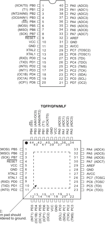
1.
Pin Configurations
Figure 1-1.
Pinout ATmega16A
(XCK/T0) PB0
(T1) PB1
(INT2/AIN0) PB2
(OC0/AIN1) PB3
(SS) PB4
(MOSI) PB5
(MISO) PB6
(SCK) PB7
RESET
VCC
GND
XTAL2
XTAL1
(RXD) PD0
(TXD) PD1
(INT0) PD2
(INT1) PD3
(OC1B) PD4
(OC1A) PD5
(ICP1) PD6
PA0 (ADC0)
PA1 (ADC1)
PA2 (ADC2)
PA3 (ADC3)
PA4 (ADC4)
PA5 (ADC5)
PA6 (ADC6)
PA7 (ADC7)
AREF
GND
AVCC
PC7 (TOSC2)
PC6 (TOSC1)
PC5 (TDI)
PC4 (TDO)
PC3 (TMS)
PC2 (TCK)
PC1 (SDA)
PC0 (SCL)
PD7 (OC2)
PA4 (ADC4)
PA5 (ADC5)
PA6 (ADC6)
PA7 (ADC7)
AREF
GND
AVCC
PC7 (TOSC2)
PC6 (TOSC1)
PC5 (TDI)
PC4 (TDO)
(MOSI) PB5
(MISO) PB6
(SCK) PB7
RESET
VCC
GND
XTAL2
XTAL1
(RXD) PD0
(TXD) PD1
(INT0) PD2
(INT1) PD3
(OC1B) PD4
(OC1A) PD5
(ICP1) PD6
(OC2) PD7
VCC
GND
(SCL) PC0
(SDA) PC1
(TCK) PC2
(TMS) PC3
PB4 (SS)
PB3 (AIN1/OC0)
PB2 (AIN0/INT2)
PB1 (T1)
PB0 (XCK/T0)
GND
VCC
P
A0 (ADC0)
P
A1 (ADC1)
P
A2 (ADC2)
P
A3 (ADC3)
PDIP
TQFP/QFN/MLF
NOTE:
Bottom pad should
be soldered to ground.
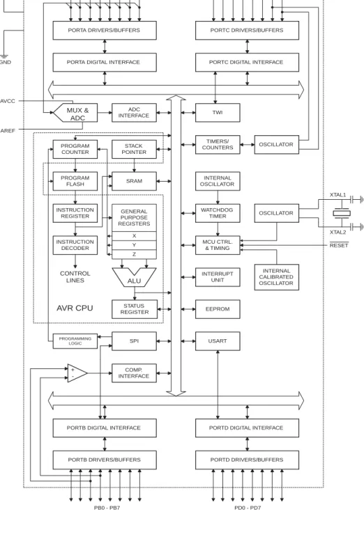
2.
Overview
The ATmega16A is a low-power CMOS 8-bit microcontroller based on the Atmel
AVR enhanced RISC
architecture. By executing powerful instructions in a single clock cycle, the ATmega16A achieves throughputs
approaching 1MIPS per MHz allowing the system designer to optimize power consumption versus processing
speed.
2.1
Block Diagram
Figure 2-1.
Block Diagram
INTERNAL OSCILLATOR OSCILLATOR WATCHDOG TIMER MCU CTRL. & TIMING OSCILLATOR TIMERS/ COUNTERS INTERRUPT UNIT STACK POINTER EEPROM SRAM STATUS REGISTER USART PROGRAM COUNTER PROGRAM FLASH INSTRUCTION REGISTER INSTRUCTION DECODER PROGRAMMING LOGIC SPI ADC INTERFACE COMP. INTERFACE PORTA DRIVERS/BUFFERS
PORTA DIGITAL INTERFACE
GENERAL PURPOSE REGISTERS X Y Z ALU + -PORTC DRIVERS/BUFFERS
PORTC DIGITAL INTERFACE
PORTB DIGITAL INTERFACE
PORTB DRIVERS/BUFFERS
PORTD DIGITAL INTERFACE
PORTD DRIVERS/BUFFERS XTAL1 XTAL2 RESET CONTROL LINES VCC GND MUX & ADC AREF PA0 - PA7 PC0 - PC7 PD0 - PD7 PB0 - PB7
AVR CPU
TWI AVCC INTERNAL CALIBRATED OSCILLATOR5
ATmega16A [DATASHEET]
Atmel-8154CS-8-bit-AVR-ATmega16A_Datasheet Summary-07/2014
The Atmel
AVR core combines a rich instruction set with 32 general purpose working registers. All the 32
registers are directly connected to the Arithmetic Logic Unit (ALU), allowing two independent registers to be
accessed in one single instruction executed in one clock cycle. The resulting architecture is more code efficient
while achieving throughputs up to ten times faster than conventional CISC microcontrollers.
The ATmega16A provides the following features: 16Kbytes of In-System Programmable Flash Program
memory with Read-While-Write capabilities; 512bytes EEPROM; 1Kbyte SRAM; 32 general purpose I/O lines,
32 general purpose working registers; a JTAG interface for Boundary-scan; On-chip Debugging support and
programming; three flexible Timer/Counters with compare modes; Internal and External Interrupts; a serial
programmable USART; a byte oriented Two-wire Serial Interface, an 8-channel; 10-bit ADC with optional
differential input stage with programmable gain (TQFP package only); a programmable Watchdog Timer with
Internal Oscillator; an SPI serial port; and six software selectable power saving modes. The Idle mode stops the
CPU while allowing the USART; Two-wire interface; A/D Converter; SRAM; Timer/Counters; SPI port; and
interrupt system to continue functioning. The Power-down mode saves the register contents but freezes the
Oscillator, disabling all other chip functions until the next External Interrupt or Hardware Reset. In Power-save
mode, the Asynchronous Timer continues to run, allowing the user to maintain a timer base while the rest of the
device is sleeping. The ADC Noise Reduction mode stops the CPU and all I/O modules except Asynchronous
Timer and ADC, to minimize switching noise during ADC conversions. In Standby mode, the crystal/resonator
Oscillator is running while the rest of the device is sleeping. This allows very fast start-up combined with
low-power consumption. In Extended Standby mode, both the main Oscillator and the Asynchronous Timer continue
to run.
The device is manufactured using Atmels high density nonvolatile memory technology. The On-chip ISP Flash
allows the program memory to be reprogrammed in-system through an SPI serial interface, by a conventional
nonvolatile memory programmer, or by an On-chip Boot program running on the AVR core. The boot program
can use any interface to download the application program in the Application Flash memory. Software in the
Boot Flash section will continue to run while the Application Flash section is updated, providing true
Read-While-Write operation. By combining an 8-bit RISC CPU with In-System Self-Programmable Flash on a
monolithic chip, the Atmel ATmega16A is a powerful microcontroller that provides a highly-flexible and
cost-effective solution to many embedded control applications.
The ATmega16A is supported with a full suite of program and system development tools including: C compilers,
macro assemblers, program debugger/simulators, in-circuit emulators, and evaluation kits.
2.2
Pin Descriptions
2.2.1
VCC
Digital supply voltage.
2.2.2
GND
Ground.
2.2.3
Port A (PA7:PA0)
Port A serves as the analog inputs to the A/D Converter.
Port A also serves as an 8-bit bi-directional I/O port, if the A/D Converter is not used. Port pins can provide
internal pull-up resistors (selected for each bit). The Port A output buffers have symmetrical drive characteristics
with both high sink and source capability. When pins PA0 to PA7 are used as inputs and are externally pulled
low, they will source current if the internal pull-up resistors are activated. The Port A pins are tri-stated when a
reset condition becomes active, even if the clock is not running.
2.2.4
Port B (PB7:PB0)
Port B is an 8-bit bi-directional I/O port with internal pull-up resistors (selected for each bit). The Port B output
buffers have symmetrical drive characteristics with both high sink and source capability. As inputs, Port B pins
that are externally pulled low will source current if the pull-up resistors are activated. The Port B pins are
tri-stated when a reset condition becomes active, even if the clock is not running.
Port B also serves the functions of various special features of the ATmega16A as listed on
page 57
.
2.2.5
Port C (PC7:PC0)
Port C is an 8-bit bi-directional I/O port with internal pull-up resistors (selected for each bit). The Port C output
buffers have symmetrical drive characteristics with both high sink and source capability. As inputs, Port C pins
that are externally pulled low will source current if the pull-up resistors are activated. The Port C pins are
tri-stated when a reset condition becomes active, even if the clock is not running. If the JTAG interface is enabled,
the pull-up resistors on pins PC5(TDI), PC3(TMS) and PC2(TCK) will be activated even if a reset occurs.
Port C also serves the functions of the JTAG interface and other special features of the ATmega16A as listed on
page 59
.
2.2.6
Port D (PD7:PD0)
Port D is an 8-bit bi-directional I/O port with internal pull-up resistors (selected for each bit). The Port D output
buffers have symmetrical drive characteristics with both high sink and source capability. As inputs, Port D pins
that are externally pulled low will source current if the pull-up resistors are activated. The Port D pins are
tri-stated when a reset condition becomes active, even if the clock is not running.
Port D also serves the functions of various special features of the ATmega16A as listed on
page 62
.
2.2.7
RESET
Reset Input. A low level on this pin for longer than the minimum pulse length will generate a reset, even if the
clock is not running. The minimum pulse length is given in
Table 27-2 on page 281
. Shorter pulses are not
guaranteed to generate a reset.
2.2.8
XTAL1
7
ATmega16A [DATASHEET]
Atmel-8154CS-8-bit-AVR-ATmega16A_Datasheet Summary-07/2014
2.2.9
XTAL2
Output from the inverting Oscillator amplifier.
2.2.10
AVCC
AVCC is the supply voltage pin for Port A and the A/D Converter. It should be externally connected to V
CC, even
if the ADC is not used. If the ADC is used, it should be connected to V
CCthrough a low-pass filter.
2.2.11
AREF
AREF is the analog reference pin for the A/D Converter.
3.
Resources
A comprehensive set of development tools, application notes and datasheets are available for download on
http://www.atmel.com/avr.
Note:
1.
Data retention
4.
Data Retention
Reliability Qualification results show that the projected data retention failure rate is much less than 1 PPM over
20 years at 85°C or 100 years at 25°C.
5.
About Code Examples
This documentation contains simple code examples that briefly show how to use various parts of the device.
These code examples assume that the part specific header file is included before compilation. Be aware that not
all C Compiler vendors include bit definitions in the header files and interrupt handling in C is compiler
6.
Register Summary
Address
Name
Bit 7
Bit 6
Bit 5
Bit 4
Bit 3
Bit 2
Bit 1
Bit 0
Page
$3F ($5F) SREG I T H S V N Z C 9
$3E ($5E) SPH – – – – – SP10 SP9 SP8 11
$3D ($5D) SPL SP7 SP6 SP5 SP4 SP3 SP2 SP1 SP0 11
$3C ($5C) OCR0 Timer/Counter0 Output Compare Register 81
$3B ($5B) GICR INT1 INT0 INT2 – – – IVSEL IVCE 47, 67
$3A ($5A) GIFR INTF1 INTF0 INTF2 – – – – – 68
$39 ($59) TIMSK OCIE2 TOIE2 TICIE1 OCIE1A OCIE1B TOIE1 OCIE0 TOIE0 82, 109, 128
$38 ($58) TIFR OCF2 TOV2 ICF1 OCF1A OCF1B TOV1 OCF0 TOV0 82, 110, 128
$37 ($57) SPMCR SPMIE RWWSB – RWWSRE BLBSET PGWRT PGERS SPMEN 242
$36 ($56) TWCR TWINT TWEA TWSTA TWSTO TWWC TWEN – TWIE 189
$35 ($55) MCUCR SM2 SE SM1 SM0 ISC11 ISC10 ISC01 ISC00 35, 66
$34 ($54) MCUCSR JTD ISC2 – JTRF WDRF BORF EXTRF PORF 41, 67, 236
$33 ($53) TCCR0 FOC0 WGM00 COM01 COM00 WGM01 CS02 CS01 CS00 79
$32 ($52) TCNT0 Timer/Counter0 (8 Bits) 81
$31(1) ($51)(1) OSCCAL Oscillator Calibration Register 30
OCDR On-Chip Debug Register 218
$30 ($50) SFIOR ADTS2 ADTS1 ADTS0 – ACME PUD PSR2 PSR10 64,84,129,194,212
$2F ($4F) TCCR1A COM1A1 COM1A0 COM1B1 COM1B0 FOC1A FOC1B WGM11 WGM10 105
$2E ($4E) TCCR1B ICNC1 ICES1 – WGM13 WGM12 CS12 CS11 CS10 107
$2D ($4D) TCNT1H Timer/Counter1 – Counter Register High Byte 108
$2C ($4C) TCNT1L Timer/Counter1 – Counter Register Low Byte 108
$2B ($4B) OCR1AH Timer/Counter1 – Output Compare Register A High Byte 109 $2A ($4A) OCR1AL Timer/Counter1 – Output Compare Register A Low Byte 109 $29 ($49) OCR1BH Timer/Counter1 – Output Compare Register B High Byte 109 $28 ($48) OCR1BL Timer/Counter1 – Output Compare Register B Low Byte 109
$27 ($47) ICR1H Timer/Counter1 – Input Capture Register High Byte 109
$26 ($46) ICR1L Timer/Counter1 – Input Capture Register Low Byte 109
$25 ($45) TCCR2 FOC2 WGM20 COM21 COM20 WGM21 CS22 CS21 CS20 125
$24 ($44) TCNT2 Timer/Counter2 (8 Bits) 127
$23 ($43) OCR2 Timer/Counter2 Output Compare Register 127
$22 ($42) ASSR – – – – AS2 TCN2UB OCR2UB TCR2UB 127
$21 ($41) WDTCR – – – WDTOE WDE WDP2 WDP1 WDP0 41
$20(2) ($40)(2) UBRRH URSEL – – – UBRR[11:8] 162
UCSRC URSEL UMSEL UPM1 UPM0 USBS UCSZ1 UCSZ0 UCPOL 161
$1F ($3F) EEARH – – – – – – – EEAR8 20
$1E ($3E) EEARL EEPROM Address Register Low Byte 20
$1D ($3D) EEDR EEPROM Data Register 20
$1C ($3C) EECR – – – – EERIE EEMWE EEWE EERE 20
$1B ($3B) PORTA PORTA7 PORTA6 PORTA5 PORTA4 PORTA3 PORTA2 PORTA1 PORTA0 64
$1A ($3A) DDRA DDA7 DDA6 DDA5 DDA4 DDA3 DDA2 DDA1 DDA0 64
$19 ($39) PINA PINA7 PINA6 PINA5 PINA4 PINA3 PINA2 PINA1 PINA0 64
$18 ($38) PORTB PORTB7 PORTB6 PORTB5 PORTB4 PORTB3 PORTB2 PORTB1 PORTB0 64
$17 ($37) DDRB DDB7 DDB6 DDB5 DDB4 DDB3 DDB2 DDB1 DDB0 64
$16 ($36) PINB PINB7 PINB6 PINB5 PINB4 PINB3 PINB2 PINB1 PINB0 65
$15 ($35) PORTC PORTC7 PORTC6 PORTC5 PORTC4 PORTC3 PORTC2 PORTC1 PORTC0 65
$14 ($34) DDRC DDC7 DDC6 DDC5 DDC4 DDC3 DDC2 DDC1 DDC0 65
$13 ($33) PINC PINC7 PINC6 PINC5 PINC4 PINC3 PINC2 PINC1 PINC0 65
$12 ($32) PORTD PORTD7 PORTD6 PORTD5 PORTD4 PORTD3 PORTD2 PORTD1 PORTD0 65
$11 ($31) DDRD DDD7 DDD6 DDD5 DDD4 DDD3 DDD2 DDD1 DDD0 65
$10 ($30) PIND PIND7 PIND6 PIND5 PIND4 PIND3 PIND2 PIND1 PIND0 65
$0F ($2F) SPDR SPI Data Register 138
$0E ($2E) SPSR SPIF WCOL – – – – – SPI2X 138
$0D ($2D) SPCR SPIE SPE DORD MSTR CPOL CPHA SPR1 SPR0 137
$0C ($2C) UDR USART I/O Data Register 158
$0B ($2B) UCSRA RXC TXC UDRE FE DOR PE U2X MPCM 159
$0A ($2A) UCSRB RXCIE TXCIE UDRIE RXEN TXEN UCSZ2 RXB8 TXB8 160
$09 ($29) UBRRL USART Baud Rate Register Low Byte 162
$08 ($28) ACSR ACD ACBG ACO ACI ACIE ACIC ACIS1 ACIS0 194
$07 ($27) ADMUX REFS1 REFS0 ADLAR MUX4 MUX3 MUX2 MUX1 MUX0 208
$06 ($26) ADCSRA ADEN ADSC ADATE ADIF ADIE ADPS2 ADPS1 ADPS0 210
$05 ($25) ADCH ADC Data Register High Byte 211
$04 ($24) ADCL ADC Data Register Low Byte 211
$03 ($23) TWDR Two-wire Serial Interface Data Register 191
$02 ($22) TWAR TWA6 TWA5 TWA4 TWA3 TWA2 TWA1 TWA0 TWGCE 192
$01 ($21) TWSR TWS7 TWS6 TWS5 TWS4 TWS3 – TWPS1 TWPS0 191
9
ATmega16A [DATASHEET]
Atmel-8154CS-8-bit-AVR-ATmega16A_Datasheet Summary-07/2014
Notes: 1. When the OCDEN Fuse is unprogrammed, the OSCCAL Register is always accessed on this address. Refer to the
debugger specific documentation for details on how to use the OCDR Register.
2. Refer to the USART description for details on how to access UBRRH and UCSRC.
3. For compatibility with future devices, reserved bits should be written to zero if accessed. Reserved I/O memory
addresses should never be written.
4. Some of the Status Flags are cleared by writing a logical one to them. Note that the CBI and SBI instructions will operate
on all bits in the I/O Register, writing a one back into any flag read as set, thus clearing the flag. The CBI and SBI
instruc-tions work with registers $00 to $1F only.
7.
Instruction Set Summary
Mnemon-ics
Operands
Description
Operation
Flags
#Clocks
ARITHMETIC AND LOGIC INSTRUCTIONSADD Rd, Rr Add two Registers Rd ← Rd + Rr Z,C,N,V,H 1
ADC Rd, Rr Add with Carry two Registers Rd ← Rd + Rr + C Z,C,N,V,H 1
ADIW Rdl,K Add Immediate to Word Rdh:Rdl ← Rdh:Rdl + K Z,C,N,V,S 2
SUB Rd, Rr Subtract two Registers Rd ← Rd - Rr Z,C,N,V,H 1
SUBI Rd, K Subtract Constant from Register Rd ← Rd - K Z,C,N,V,H 1
SBC Rd, Rr Subtract with Carry two Registers Rd ← Rd - Rr - C Z,C,N,V,H 1 SBCI Rd, K Subtract with Carry Constant from Reg. Rd ← Rd - K - C Z,C,N,V,H 1 SBIW Rdl,K Subtract Immediate from Word Rdh:Rdl ← Rdh:Rdl - K Z,C,N,V,S 2
AND Rd, Rr Logical AND Registers Rd ← Rd • Rr Z,N,V 1
ANDI Rd, K Logical AND Register and Constant Rd ← Rd • K Z,N,V 1
OR Rd, Rr Logical OR Registers Rd ← Rd v Rr Z,N,V 1
ORI Rd, K Logical OR Register and Constant Rd ← Rd v K Z,N,V 1
EOR Rd, Rr Exclusive OR Registers Rd ← Rd ⊕ Rr Z,N,V 1
COM Rd One’s Complement Rd ← $FF − Rd Z,C,N,V 1
NEG Rd Two’s Complement Rd ← $00 − Rd Z,C,N,V,H 1
SBR Rd,K Set Bit(s) in Register Rd ← Rd v K Z,N,V 1
CBR Rd,K Clear Bit(s) in Register Rd ← Rd • ($FF - K) Z,N,V 1
INC Rd Increment Rd ← Rd + 1 Z,N,V 1
DEC Rd Decrement Rd ← Rd − 1 Z,N,V 1
TST Rd Test for Zero or Minus Rd ← Rd • Rd Z,N,V 1
CLR Rd Clear Register Rd ← Rd ⊕ Rd Z,N,V 1
SER Rd Set Register Rd ← $FF None 1
MUL Rd, Rr Multiply Unsigned R1:R0 ← Rd x Rr Z,C 2
MULS Rd, Rr Multiply Signed R1:R0 ← Rd x Rr Z,C 2
MULSU Rd, Rr Multiply Signed with Unsigned R1:R0 ← Rd x Rr Z,C 2
FMUL Rd, Rr Fractional Multiply Unsigned R1:R0 ← (Rd x Rr) << 1 Z,C 2 FMULS Rd, Rr Fractional Multiply Signed R1:R0 ← (Rd x Rr) << 1 Z,C 2 FMULSU Rd, Rr Fractional Multiply Signed with Unsigned R1:R0 ← (Rd x Rr) << 1 Z,C 2 BRANCH INSTRUCTIONS
RJMP k Relative Jump PC ← PC + k + 1 None 2
IJMP Indirect Jump to (Z) PC ← Z None 2
JMP k Direct Jump PC ← k None 3
RCALL k Relative Subroutine Call PC ← PC + k + 1 None 3
ICALL Indirect Call to (Z) PC ← Z None 3
CALL k Direct Subroutine Call PC ← k None 4
RET Subroutine Return PC ← STACK None 4
RETI Interrupt Return PC ← STACK I 4
CPSE Rd,Rr Compare, Skip if Equal if (Rd = Rr) PC ← PC + 2 or 3 None 1 / 2 / 3
CP Rd,Rr Compare Rd − Rr Z, N,V,C,H 1
CPC Rd,Rr Compare with Carry Rd − Rr − C Z, N,V,C,H 1
CPI Rd,K Compare Register with Immediate Rd − K Z, N,V,C,H 1
SBRC Rr, b Skip if Bit in Register Cleared if (Rr(b)=0) PC ← PC + 2 or 3 None 1 / 2 / 3 SBRS Rr, b Skip if Bit in Register is Set if (Rr(b)=1) PC ← PC + 2 or 3 None 1 / 2 / 3 SBIC P, b Skip if Bit in I/O Register Cleared if (P(b)=0) PC ← PC + 2 or 3 None 1 / 2 / 3 SBIS P, b Skip if Bit in I/O Register is Set if (P(b)=1) PC ← PC + 2 or 3 None 1 / 2 / 3 BRBS s, k Branch if Status Flag Set if (SREG(s) = 1) then PC←PC+k + 1 None 1 / 2 BRBC s, k Branch if Status Flag Cleared if (SREG(s) = 0) then PC←PC+k + 1 None 1 / 2
BREQ k Branch if Equal if (Z = 1) then PC ← PC + k + 1 None 1 / 2
BRNE k Branch if Not Equal if (Z = 0) then PC ← PC + k + 1 None 1 / 2
BRCS k Branch if Carry Set if (C = 1) then PC ← PC + k + 1 None 1 / 2
BRCC k Branch if Carry Cleared if (C = 0) then PC ← PC + k + 1 None 1 / 2 BRSH k Branch if Same or Higher if (C = 0) then PC ← PC + k + 1 None 1 / 2
BRLO k Branch if Lower if (C = 1) then PC ← PC + k + 1 None 1 / 2
BRMI k Branch if Minus if (N = 1) then PC ← PC + k + 1 None 1 / 2
BRPL k Branch if Plus if (N = 0) then PC ← PC + k + 1 None 1 / 2
BRGE k Branch if Greater or Equal, Signed if (N ⊕ V= 0) then PC ← PC + k + 1 None 1 / 2 BRLT k Branch if Less Than Zero, Signed if (N ⊕ V= 1) then PC ← PC + k + 1 None 1 / 2 BRHS k Branch if Half Carry Flag Set if (H = 1) then PC ← PC + k + 1 None 1 / 2 BRHC k Branch if Half Carry Flag Cleared if (H = 0) then PC ← PC + k + 1 None 1 / 2
BRTS k Branch if T Flag Set if (T = 1) then PC ← PC + k + 1 None 1 / 2
11
ATmega16A [DATASHEET]
Atmel-8154CS-8-bit-AVR-ATmega16A_Datasheet Summary-07/2014
BRVS k Branch if Overflow Flag is Set if (V = 1) then PC ← PC + k + 1 None 1 / 2 BRVC k Branch if Overflow Flag is Cleared if (V = 0) then PC ← PC + k + 1 None 1 / 2 BRIE k Branch if Interrupt Enabled if ( I = 1) then PC ← PC + k + 1 None 1 / 2 BRID k Branch if Interrupt Disabled if ( I = 0) then PC ← PC + k + 1 None 1 / 2 DATA TRANSFER INSTRUCTIONS
MOV Rd, Rr Move Between Registers Rd ← Rr None 1
MOVW Rd, Rr Copy Register Word Rd+1:Rd ← Rr+1:Rr None 1
LDI Rd, K Load Immediate Rd ← K None 1
LD Rd, X Load Indirect Rd ← (X) None 2
LD Rd, X+ Load Indirect and Post-Inc. Rd ← (X), X ← X + 1 None 2
LD Rd, - X Load Indirect and Pre-Dec. X ← X - 1, Rd ← (X) None 2
LD Rd, Y Load Indirect Rd ← (Y) None 2
LD Rd, Y+ Load Indirect and Post-Inc. Rd ← (Y), Y ← Y + 1 None 2
LD Rd, - Y Load Indirect and Pre-Dec. Y ← Y - 1, Rd ← (Y) None 2
LDD Rd,Y+q Load Indirect with Displacement Rd ← (Y + q) None 2
LD Rd, Z Load Indirect Rd ← (Z) None 2
LD Rd, Z+ Load Indirect and Post-Inc. Rd ← (Z), Z ← Z+1 None 2
LD Rd, -Z Load Indirect and Pre-Dec. Z ← Z - 1, Rd ← (Z) None 2
LDD Rd, Z+q Load Indirect with Displacement Rd ← (Z + q) None 2
LDS Rd, k Load Direct from SRAM Rd ← (k) None 2
ST X, Rr Store Indirect (X) ← Rr None 2
ST X+, Rr Store Indirect and Post-Inc. (X) ← Rr, X ← X + 1 None 2
ST - X, Rr Store Indirect and Pre-Dec. X ← X - 1, (X) ← Rr None 2
ST Y, Rr Store Indirect (Y) ← Rr None 2
ST Y+, Rr Store Indirect and Post-Inc. (Y) ← Rr, Y ← Y + 1 None 2
ST - Y, Rr Store Indirect and Pre-Dec. Y ← Y - 1, (Y) ← Rr None 2
STD Y+q,Rr Store Indirect with Displacement (Y + q) ← Rr None 2
ST Z, Rr Store Indirect (Z) ← Rr None 2
ST Z+, Rr Store Indirect and Post-Inc. (Z) ← Rr, Z ← Z + 1 None 2
ST -Z, Rr Store Indirect and Pre-Dec. Z ← Z - 1, (Z) ← Rr None 2
STD Z+q,Rr Store Indirect with Displacement (Z + q) ← Rr None 2
STS k, Rr Store Direct to SRAM (k) ← Rr None 2
LPM Load Program Memory R0 ← (Z) None 3
LPM Rd, Z Load Program Memory Rd ← (Z) None 3
LPM Rd, Z+ Load Program Memory and Post-Inc Rd ← (Z), Z ← Z+1 None 3
SPM Store Program Memory (Z) ← R1:R0 None
-IN Rd, P In Port Rd ← P None 1
OUT P, Rr Out Port P ← Rr None 1
PUSH Rr Push Register on Stack STACK ← Rr None 2
POP Rd Pop Register from Stack Rd ← STACK None 2
BIT AND BIT-TEST INSTRUCTIONS
SBI P,b Set Bit in I/O Register I/O(P,b) ← 1 None 2
CBI P,b Clear Bit in I/O Register I/O(P,b) ← 0 None 2
LSL Rd Logical Shift Left Rd(n+1) ← Rd(n), Rd(0) ← 0 Z,C,N,V 1
LSR Rd Logical Shift Right Rd(n) ← Rd(n+1), Rd(7) ← 0 Z,C,N,V 1
ROL Rd Rotate Left Through Carry Rd(0)←C,Rd(n+1)← Rd(n),C←Rd(7) Z,C,N,V 1 ROR Rd Rotate Right Through Carry Rd(7)←C,Rd(n)← Rd(n+1),C←Rd(0) Z,C,N,V 1
ASR Rd Arithmetic Shift Right Rd(n) ← Rd(n+1), n=0:6 Z,C,N,V 1
SWAP Rd Swap Nibbles Rd(3:0)←Rd(7:4),Rd(7:4)←Rd(3:0) None 1
BSET s Flag Set SREG(s) ← 1 SREG(s) 1
BCLR s Flag Clear SREG(s) ← 0 SREG(s) 1
BST Rr, b Bit Store from Register to T T ← Rr(b) T 1
BLD Rd, b Bit load from T to Register Rd(b) ← T None 1
SEC Set Carry C ←1 C 1
CLC Clear Carry C ← 0 C 1
SEN Set Negative Flag N ←1 N 1
CLN Clear Negative Flag N ← 0 N 1
SEZ Set Zero Flag Z ←1 Z 1
CLZ Clear Zero Flag Z ← 0 Z 1
SEI Global Interrupt Enable I ←1 I 1
CLI Global Interrupt Disable I ← 0 I 1
SES Set Signed Test Flag S ←1 S 1
CLS Clear Signed Test Flag S ← 0 S 1
SEV Set Twos Complement Overflow. V ←1 V 1
CLV Clear Twos Complement Overflow V ← 0 V 1
SET Set T in SREG T ←1 T 1
Mnemon-ics
Operands
Description
Operation
Flags
CLT Clear T in SREG T ← 0 T 1
SEH Set Half Carry Flag in SREG H ←1 H 1
CLH Clear Half Carry Flag in SREG H ← 0 H 1
MCU CONTROL INSTRUCTIONS
NOP No Operation None 1
SLEEP Sleep (see specific descr. for Sleep function) None 1
WDR Watchdog Reset (see specific descr. for WDR/timer) None 1
BREAK Break For On-Chip Debug Only None N/A
Mnemon-ics
Operands
Description
Operation
Flags
13
ATmega16A [DATASHEET]
Atmel-8154CS-8-bit-AVR-ATmega16A_Datasheet Summary-07/2014
8.
Ordering Information
Notes: 1. Pb-free packaging complies to the European Directive for Restriction of Hazardous Substances (RoHS directive). Also
Halide free and fully Green.
2. Tape & Reel.
Speed (MHz)
Power Supply
Ordering Code
(1)Package
Operation Range
16
2.7 - 5.5V
ATmega16A-AU
ATmega16A-AUR
(2)ATmega16A-PU
ATmega16A-MU
ATmega16A-MUR
(2)44A
44A
40P6
44M1
44M1
Industrial
(-40
oC to 85
oC)
Package Type
44A
44-lead, Thin (1.0 mm) Plastic Gull Wing Quad Flat Package (TQFP)
40P6
40-pin, 0.600” Wide, Plastic Dual Inline Package (PDIP)
9.
Packaging Information
9.1
44A
44A,
44-lead, 10 x 10mm
b
ody size, 1.0mm
b
ody thickness,
0.8 mm lead pitch, thin profile plastic q
u
ad flat package (TQFP)
44A
C
06/02/2014
PIN 1 IDENTIFIER0°~7°
PI
N
1
L
C
A1
A2
A
D1
D
e
E1
E
B
COMMON DIMENSIONS (Unit of Measure = mm)SYMBOL MIN NOM MAX NOTE
Notes:
1. This package conforms to JEDEC reference MS-026, Variation ACB. 2. Dimensions D1 and E1 do not include mold protrusion. Allowable protrusion is 0.25mm per side. Dimensions D1 and E1 are maximum plastic body size dimensions including mold mismatch.
3. Lead coplanarity is 0.10mm maximum.
A – – 1.20 A1 0.05 – 0.15 A2 0.95 1.00 1.05 D 11.75 12.00 12.25 D1 9.90 10.00 10.10 Note 2 E 11.75 12.00 12.25 E1 9.90 10.00 10.10 Note 2 B 0.30 0.37 0.45 C 0.09 (0.17) 0.20 L 0.45 0.60 0.75 e 0.80 TYP
15
ATmega16A [DATASHEET]
Atmel-8154CS-8-bit-AVR-ATmega16A_Datasheet Summary-07/20149.2
40P6
PI
N
1
E1
A1
B
REF
E
B1
C
L
SEATING PLANEA
0º ~ 15º
D
e
eB
COMMON DIMENSIONS
(Unit of Meas
u
re = mm)
SYMBOL
MIN
NOM
MAX
NOTE
A
–
–
4.826
A1
0.381
–
–
D
52.070
–
52.578 Note 2
E
15.240
–
15.875
E1
13.462
–
13.970 Note 2
B
0.356
–
0.559
B1
1.041
–
1.651
L
3.048
–
3.556
C
0.203
–
0.381
eB
15.494
–
17.526
e
2.540 TYP
1. This package conforms to JEDEC reference MS-011, Variation AC.
2. Dimensions D and E1 do not include mold Flash or Protrusion.
Mold Flash or Protrusion shall not exceed 0.25mm (0.010
"
).
Notes:
40P6
, 40-lead (0.600"/15.24mm Wide) Plastic D
u
al
Inline Package (PDIP)
40P6
C
9.3
44M1
TITLE
GPC
DRAWING NO.
REV.
Package Drawing Contact:
[email protected]
ZWS
44M1
H
44M1,
44-pad, 7 x 7 x 1.0mm body, lead
pitch 0.50mm, 5.20mm exposed pad, thermally
enhanced plastic very thin quad flat no
lead package (VQFN)
02/13/2014
COMMON DIMENSIONS
(Unit of Measure = mm)
SYMBOL
MIN
NOM
MAX
NOT E
A
0.80
0.90
1.00
A1
–
0.02
0.05
A3
0.20 REF
b
0.18
0.23
0.30
D
D2
5.00
5.20
5.40
6.90
7.00
7.10
6.90
7.00
7.10
E
E2
5.00
5.20
5.40
e
0.50 BSC
L
0.59
0.64
0.69
K
0.20
0.26
0.41
Note: JEDEC Standard MO-220, Fig . 1 (S AW Singulation) VKKD-3 .TOP VIE W
SIDE VIEW
B OT TOM VIE W
D
E
Ma rked Pin# 1 I DE2
D2
b
e
Pin #1 Co rnerL
A1
A3
A
SE ATING PLAN E Pin #1 Triangle Pin #1 Cham fer (C 0.30) Option A Option B Pin #1 Notch (0.20 R) Option CK
K
1 2 317
ATmega16A [DATASHEET]
Atmel-8154CS-8-bit-AVR-ATmega16A_Datasheet Summary-07/2014
10.
Errata
The revision letter in this section refers to the revision of the ATmega16A device.
10.1
ATmega16A rev. N to rev. Q
•
First Analog Comparator conversion may be delayed
•
Interrupts may be lost when writing the timer registers in the asynchronous timer
•
IDCODE masks data from TDI input
•
Reading EEPROM by using ST or STS to set EERE bit triggers unexpected interrupt request
1.
First Analog Comparator conversion may be delayed
If the device is powered by a slow rising V
CC, the first Analog Comparator conversion will take longer than
expected on some devices.
Problem Fix/Workaround
When the device has been powered or reset, disable then enable theAnalog Comparator before the first
conversion.
2.
Interrupts may be lost when writing the timer registers in the asynchronous timer
The interrupt will be lost if a timer register that is synchronous timer clock is written when the asynchronous
Timer/Counter register (TCNTx) is 0x00.
Problem Fix/Workaround
Always check that the asynchronous Timer/Counter register neither have the value 0xFF nor 0x00 before
writing to the asynchronous Timer Control Register (TCCRx), asynchronous Timer Counter Register
(TCNTx), or asynchronous Output Compare Register (OCRx).
3.
IDCODE masks data from TDI input
The JTAG instruction IDCODE is not working correctly. Data to succeeding devices are replaced by all-ones
during Update-DR.
Problem Fix / Workaround
–
If ATmega16A is the only device in the scan chain, the problem is not visible.
–
Select the Device ID Register of the ATmega16A by issuing the IDCODE instruction or by entering
the Test-Logic-Reset state of the TAP controller to read out the contents of its Device ID Register
and possibly data from succeeding devices of the scan chain. Issue the BYPASS instruction to the
ATmega16A while reading the Device ID Registers of preceding devices of the boundary scan chain.
–
If the Device IDs of all devices in the boundary scan chain must be captured simultaneously, the
ATmega16A must be the fist device in the chain.
4.
Reading EEPROM by using ST or STS to set EERE bit triggers unexpected interrupt request.
Reading EEPROM by using the ST or STS command to set the EERE bit in the EECR register triggers an
unexpected EEPROM interrupt request.
Problem Fix / Workaround
11.
Datasheet Revision History
Please note that the referring page numbers in this section are referred to this document. The referring revision
in this section are referring to the document revision.
Rev. 8154C –07/2014
Rev. 8154B – 07/09
Rev. 8154A – 06/08
1.
Atmel brand style guide and datasheet template of 2014-0502 updated in datasheet including
the last page.
2.
Updated the Ordering Code to include Tape & Reel part numbers.
3.
Removed notes 6 and 7 concerning actual low period in
Table 27-4 on page 282
.
4.
Changed notes 3, 4 and 5, removed note 6 concerning TQFP/MLF packages in
“DC Characteristics” on page 278
Section 27.2
1. Updated
“Errata” on page 17
.
2.
Updated the last page with Atmel’s new addresses.
1.
Initial revision (Based on the ATmega16/L datasheet revision 2466R-AVR-05/08)
Changes done compared ATmega16/L datasheet revision 2466R-AVR-05/08:
- Updated description in
“Stack Pointer” on page 11
.
- All Electrical characteristics is moved to
“Electrical Characteristics” on page 278
.
- Register descriptions are moved to sub sections at the end of each chapter.
- Added
“Speed Grades” on page 280
.
- New graphs in
“Typical Characteristics” on page 289
.
- New
“Ordering Information” on page 13
.
X
X X
X
X
X
Atmel Corporation 1600 Technology Drive, San Jose, CA 95110 USA T: (+1)(408) 441.0311 F: (+1)(408) 436.4200 | www.atmel.com © 2014 Atmel Corporation. / Rev.: Atmel-8154CS-8-bit-AVR-ATmega16A_Datasheet Summary-07/2014.
Atmel®, Atmel logo and combinations thereof, Enabling Unlimited Possibilities®, AVR® and others are registered trademarks or trademarks of Atmel Corporation in U.S. and other countries. Other terms and product names may be trademarks of others.
DISCLAIMER: The information in this document is provided in connection with Atmel products. No license, express or implied, by estoppel or otherwise, to any intellectual property right is granted by this document or in connection with the sale of Atmel products. EXCEPT AS SET FORTH IN THE ATMEL TERMS AND CONDITIONS OF SALES LOCATED ON THE ATMEL WEBSITE, ATMEL ASSUMES NO LIABILITY WHATSOEVER AND DISCLAIMS ANY EXPRESS, IMPLIED OR STATUTORY WARRANTY RELATING TO ITS PRODUCTS INCLUDING, BUT NOT LIMITED TO, THE IMPLIED WARRANTY OF MERCHANTABILITY, FITNESS FOR A PARTICULAR PURPOSE, OR NON-INFRINGEMENT. IN NO EVENT SHALL ATMEL BE LIABLE FOR ANY DIRECT, INDIRECT, CONSEQUENTIAL, PUNITIVE, SPECIAL OR INCIDENTAL DAMAGES (INCLUDING, WITHOUT LIMITATION, DAMAGES FOR LOSS AND PROFITS, BUSINESS INTERRUPTION, OR LOSS OF INFORMATION) ARISING OUT OF THE USE OR INABILITY TO USE THIS DOCUMENT, EVEN IF ATMEL HAS BEEN ADVISED OF THE POSSIBILITY OF SUCH DAMAGES. Atmel makes no representations or warranties with respect to the accuracy or completeness of the contents of this document and reserves the right to make changes to specifications and products descriptions at any time without notice. Atmel does not make any commitment to update the information contained herein. Unless specifically provided otherwise, Atmel products are not suitable for, and shall not be used in, automotive applications. Atmel products are not intended, authorized, or warranted for use as components in applications intended to support or sustain life.
SAFETY-CRITICAL, MILITARY, AND AUTOMOTIVE APPLICATIONS DISCLAIMER: Atmel products are not designed for and will not be used in connection with any applications where the failure of such products would reasonably be expected to result in significant personal injury or death (“Safety-Critical Applications”) without an Atmel officer's specific written consent. Safety-Critical Applications include, without limitation, life support devices and systems, equipment or systems for the operation of nuclear facilities and weapons systems. Atmel products are not designed nor intended for use in military or aerospace applications or environments unless specifically designated by Atmel as military-grade. Atmel products are not designed nor intended for use in automotive applications unless specifically designated by Atmel as automotive-grade.