e-ISSN: 2278-7461, p-ISSN: 2319-6491
Volume 5, Issue 07 [Aug. 2016] PP: 01-06
Thermal Emittance and Solar absorptance of cds Thin Films
Mosiori, Cliff Orori
*1; Kwembur, Morko Isaac
*1; Maera, John
*2Department of Mathematics and Physics, Technical University of Mombasa, P. O Box 90420 - 80100, Kenya
*1Department of Physics, Kenyatta University, Box 43844-0100, Nairobi
ABSTRACT: CdS thin films were grown on highly cleaned substrates of Microscope glass slides using solution deposition technique at different molar concentrations at constant time and repeated at a fixed molar concentration at for different deposition times. Measurement of the thermal emittance on polished and coated substrates was determined before and after growth. The average thermal emittance value of polished uncoated sample plate was 0.152 with an error of ± 0.013 while an average thermal emittance value of the coated sample was 0.15 ± 0.01. Equally when the average solar absorptance values of the coated sample plate substrate was 0.473 with an error of ± 0.01. Thin film thickness varied from 0.212 - 0.614 µm with an error of ± 0.01. These outcomes formed the basis for proposing these thin films as appropriate for photothermal solar energy application.
KEYWORDS: Thermal emittance, solar absorptance, solar thermal devices.
I.
INTRODUCTION
The major aim of many solar energy researches done on semiconductor thin films to find out which characteristics are good enough for fabricating good selective absorbers (Sharma et al., 1988); Granziera, (1977); Ilenikhena, and Mordi, 2005; Ilenikhena, 2008). Solution processing has become one of the basic technique for depositing binary and ternary sulphides and selenides (Ezekoye, & Okeke, 1997; Ndukwe, (1992); Ezema and Okeke, (2003); Chopra, and Das, (1983); Ezekoye and Okeke, (2005); Okoli et al., 2006) that produce comparable structural and photoelectric properties for many solar energy applications (Ilenikhena and Okeke, (2004); Ezema and Okeke, (2003); Ilenikehna, and Mordi, 2005). This method is basic since it is a low cost and ease handling method for large surface applicability based on a slowly controlled precipitation of the desired compound from its ions in a reaction bath in the presence of a complexing agent. This study investigated absorptance and thermal emittance of solution grown cadmium sulphide thin films grown on Microscope glass slides.
II.
THEORY
In a slowly controlled precipitation, a compound is deposited when its ionic product is greater than the solubility product Ksp (Lange, 1992) by using a complexing agent. The complexing agent forms stable complex ions of the
metal and also provides a controlled number of free ions according to an equilibrium reaction as follows: A
M A
B( )2 2 (1)
where the symbol, M2+ represents the metal ion while the symbol, A represents the complexing agent. Therefore, the dissociation constant of an ion at any temperature is given by;
KdA M
A M
2 2
(2)
where, Kd is dissociation constant of a complex ion (Chopra, and Das, 1983).
III.
METHODODLOGY
3.1 Preparation of Substrates
Microscope glass slides substrates were cleaned, decreased and thoroughly washed with distilled water until the required mirror finishing was obtained. The polished plates were re-washed with distilled water, allowed to dry at room temperature and marked with numbers for identification. The growth bath was a 500ml glass beaker.
3.2 Preparation of Solution
1000
V W M
m (3)
where, M is the required molar concentration, m is the mass to be dissolved, W is the molar mass of the chemical reagent and V is the volume of distilled water. Aqueous solution of 1.0M of cadmium sulphide, 4.0M of ammonia, 2.5M of sodium hydroxide and 1.0M of thourea as the complexing agent constituted the bath solution.
3.3 Experimental Procedures
Pre-test runs were carried out to ensure optimum deposition conditions by using different volumes to obtain the required molar concentration of cadmium sulphide in solution. The twenty four (24) polished substrates in pairs of four each were used at a time using 0.04, 0.08, 0.12, 0.16, 0.20 and 0.24 molar concentration of optimum cadmium sulphide precursor solutions for a deposition time of 24 hours. It was repeated for 0.24 molar concentrations of cadmium sulphide precursor solutions for varying deposition times and as-grown CdS thin films were rinsed with distilled water, drip dried and kept for characterization.
IV.
RESULTS AND DISCUSSIONS
4.1 Growth Mechanisms
Dissociation reactions and controlled release of ions according to the equation below form the CdS precipitate (Mosiori et al., 2014; Sharma, and Hutchin (1979)
:
CdCl 2(aq) 2NH 3(aq)
Cd (NH 3)2
Cl2(aq) (4)
( ) 3( ) 2( )2
) ( 2 2
3) 2
(NH Cl aq Cd aq NH g Cl g
Cd (5)
(NH 2)2C(s)
OH (aq) CH 2N2(aq) H2O(l)
(6)
) ( ) ( 2 )
( )
(
5 aq OH aq H O l 5O g
H (7)
The overall equation (Ezema, and Okeke (2003) for the chemical reaction is:
) ( 2 ) ( 2 ) ( 2 2 ) ( )
( )
( 2 3 )
( 3 )
(
2 aq 2NH aq (NH ) CS aq 2OH aq CdS s CH N aq Cl g 2H O l
CdCl (8)
The source of the S2- ions is thourea and thus the precipitation occurs as (Mosiori et al., 2014):
Cd 2 S2 CdS (9)
4.2 Measurement of film thickness
The CdS thin film thickness of the deposited thin films was calculated using the expression (Mosiori, and
Maera, (2015); Mosiori et al., 2015):
A m T
2
(10)
where, m is the mass of the thin film deposited and was obtained from the difference in mass of each of the sample before and after film deposition, A is the area of film on the sample and ρ= 4.82g/cm3 is the theoretical density of cadmium sulphide (CdS).
4.3 Measurement of Thermal Emittance using Emissiometer
The measurement of the thermal emittance with the deposited CdS thin films was determined by an emission meter (or emissiometer) consisting of a radiation detector and heat sink. The emissiometer output was obtained in millivolts and calibrated by a black standard sample plate of polished aluminium and black standard plate (e= 0.93). Where 0.93 is the thermal emittance of a standard black surface, the values for each of the thermal emittance of the sample plates where calculated from the formula:
dard S Sample thermal
V V e
tan
93 . 0
(11)
4.4 Measurement of Solar Absorptance using Alphatometer
The measurement of the solar absorptance (αs) were taken and the reflectance, r, calculated using an
) ( Re ..
) ( Re .. Re
I ading Incident
R ading lected
output V V
G (12)
The quoted accuracies of the emittance and absorptance are the standard deviations of the mean and are within the error limits of the instruments used (Ilenikhena, Okeke (2002); Ilenikhena, and Mordi (2005); Mosiori et al.,
(2015); Mosiori, (2013)). Therefore the solar absorptance (αs) was then calculated from the formula:
αs = 1 – r (13)
The results were tabulated in table 1 for unpolished substrates and table 2 for polished substrates. Thermal emittance and Solar absorptance for uncoated polished lass slides of sample plates for different molar concentrations of CdS in deposition bath for deposition time of 24 hours is 0.15 ± 0.01and 0.47 ± 0.01respectively were tabulated in table 2 while that for uncoated sample plates of glass slides for 0.24 molar concentrations of CdS in deposition bath for different deposition times is 0.15 ± 0.01and 0.47 ± 0.01 and were also tabulated in table 1.
Table 1: Solar absorptance (αs), thermal emittance and film thickness for polished substrates
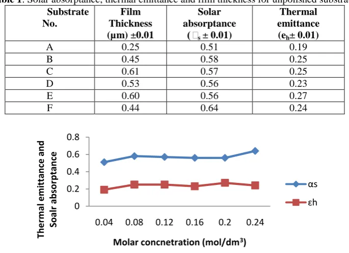
This thermal emittance result compares well with the thermal emittance value of 0.13 to 0.17 ± 0.01 for polished using abrasives of different grain sizes (Sharma, 1982). Table 2 and Figure 1 show the thermal emittance values of the coated sample plates increased slightly from 0.15 to 0.27 ± 0.01 and solar absorptance values also increased greatly from 0.47 to 0.64 ± 0.01 for increased molar concentration of CdS in bath solution at 24 hours deposition time.
Table 1: Solar absorptance, thermal emittance and film thickness for unpolished substrates Substrate
No.
Film Thickness (µm) ±0.01
Solar absorptance
( αs ± 0.01)
Thermal emittance (eh± 0.01)
A 0.25 0.51 0.19
B 0.45 0.58 0.25
C 0.61 0.57 0.25
D 0.53 0.56 0.23
E 0.60 0.56 0.27
F 0.44 0.64 0.24
Figure 1. Variation of Thermal emittance and solar absorptance of CdS film with Molar concentration
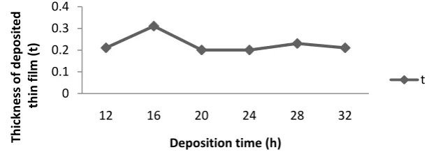
As shown in Fig 2, there was a gradual increase in film thickness from 0.27 to 0.61µm ±0.01 for increase in molar concentration of 0.04 to 0.12 and a slight decrease in thickness of 0.60 to 0.44µm ±0.01 for
0 0.2 0.4 0.6 0.8
0.04 0.08 0.12 0.16 0.2 0.24
Th
e
rm
al
e
m
itt
an
ce
an
d
So
al
r
ab
sor
p
tan
ce
Molar concnetration (mol/dm3)
αs
ɛh Substrate
No.
Film Thickness (µm) ±0.01
Solar absorptance ( αs ± 0.01)
Thermal emittance (eh± 0.01)
A 0.21 0.48 0.19
B 0.31 0.55 0.24
C 0.20 0.57 0.23
D 0.20 0.50 0.22
E 0.23 0.55 0.21
plates increased slightly from 0.15 to 0.25 ± 0.01 and solar absorptance values also increased greatly from 0.47 to 0.57 ± 0.01 for 0.24 molar concentrations of CdS in bath solution at different deposition times. This was plotted in figure 2. These results show that thermal emittance values of deposited CdS thin films on glass slides are low and can be compared to thermal emiitance values of oxidized glass slides selective surfaces which are used for photothermal conversion of solar energy. The most favourable thermal emittance values of 0.19 ± 0.01 compare to 0.18 ± 0.01 for oxidized glass slides selective surfaces (Sharma et al., 1988) and also the solar absorptance of 0.64 ±0.01 were obtained with film thickness of 0.44µm ± 0.01 with 0.24 molar concentration of CdS in bath solution at deposition time of 24 hours.
Figure 2: Variation of Thickness of deposited CdS thin film molar concentration
Figure 3: Variation of Thermal emittance and solar absorptance of CdS film with Deposition time
Figure 4 shows a great increase of deposited thin film thickness of 0.21 to 0.31µm ±0.01. The coatings help to modify the micro structure and composition of the absorber plate so as to provide higher absorbance for the wavelength range of 0.3 to 2.5µm (Sharma et al., 1988). The thickness of the thin film deposited could be hardened to withstand adverse weather condition and degradation thus prolonging the lifespan of the absorber surface (Eze, and Okeke (1997); Ezekye, and Okeke (2005) Ezema, and Okeke (2003)). Their corresponding film thicknesses vary from 0.25 to 0.60µm ±0.01. Thin films deposited with 0.24 molar concentrations at varying deposition times has thermal emittance value of coated plate vary from 0.19 to 0.25 ±0.01 and solar absorptance value of 0.48 to 0.57 ±0.01 with film thickness of 0.21 to 0.31 µm ±0.01.
Figure 4. Variation of Thickness of deposited thin film with Deposition time
The coated sample plates with most favourable condition which could be employed for solar thermal devices has thermal emittance value of 0.24 ±0.01, solar absorptance value of 0.64 ±0.01 and thin film thickness of
0 0.2 0.4 0.6 0.8
0.04 0.08 0.12 0.16 0.2 0.24
Th
ic
kn
e
ss
o
f
d
e
p
o
si
te
d
th
in
fi
lm
(µ
m
)
Molar concentration (mol/dm3)
t
0 0.1 0.2 0.3 0.4 0.5 0.6
12 16 20 24 28 32
Th
e
rm
al
e
m
itt
an
ce
an
d
So
al
r
ab
sor
p
tan
ce
Depsotion time (h)
αs
ɛh
0 0.1 0.2 0.3 0.4
12 16 20 24 28 32
Th
ic
kn
e
ss
o
f d
e
p
o
si
te
d
th
in
fi
lm
(t
)
Deposition time (h)
0.12µm ±0.01 for 0.24 molar concentration of CdS in solution bath at deposition time of 24 hours. Therefore, solution growth method could be used to grow thin films for applications in photothermal conversion of solar energy.
V.
CONCLUSION
Cadmium Sulphide thin films were deposited on polished Microscope glass slides of sample plates using solution growth method at different molar concentration for deposition time of 24 hours. An emissiometer was used to determine the thermal emittance values of the sample plates before and after thin film deposition. An alphatometer was used to determine the solar absorptance values of the sample plates before and after thin film deposition. The average thermal emittance of the polished sample plates is 0.15 ±0.01 and the average solar absorptance value for polished sample plate is 0.47 ±0.01. The values of thermal emittance of the coated plates vary from 0.19 to 0.27 ±0.01 and the absorptance from 0.51 to 0.64 ±0.01. Their corresponding film thicknesses vary from 0.25 to 0.60µm ±0.01. The thin films could be employed for solar thermal devices has thermal emittance value of 0.24 ±0.01, solar absorptance value of 0.64 ±0.01 and thin film thickness of 0.12µm ±0.01 for 0.24 molar concentration of CdS in solution bath at deposition time of 24 hours.
VI.
ACKNOWLEDGEMENT
The author is thankful Department of Mathematics and Physics of Technical University of Mombasa, Mombasa for providing laboratory facilities that enabled this work to be completed.
REFERENCES
[1] Chopra, K.L and Das, S.R (1983). Thin Film Solar Cells. Plenium Press: New York
[2] Eze, F.C and Okeke, C.E. (1997). Chemical Bath Depsotied Cobalt Sulphide Films; Preparation Effects. Mater. Chem. Phys., 47:31-36
[3] Ezekye, B.A. and Okeke, C.E (2005). Optical Properties in PbHgS ternary Thin Films Deposited by the Solution Growth Method, Pacific J. Sci. Tech. 6(1):23-28
[4] Ezema F.I and Okeke, C.E. (2003). Fabrication and Characterization of Palladium Sulphide (PdS) Thin Films for Solar Energy Applications using Solution Growth Technique, Nig. J. Solar energy, 14: 66-72. [5] Ezema, F.I and. Okeke, C.E. (2003). Chemical Bath Deposition of Bismuth Oxide (Bi2O3) Thin Film and
its Application, Greenwich J. Sci. Tech. 3; 90-109
[6] Grazeria, F. (1977). Coloured Microscope glass slides in Solar Energy Collectors, Aluminium Anodizers Pty Ltd., Australasia, 211.
[7] Ilenikhena, P.A .(2008). Optical Characterization and Possible Solar Energy Applications of Improved Solution Grown Cobalt Oxide (CoO) Thin Films, Afr. Physical Rev., 2: 0008, 68-77.
[8] Ilenikhena, P.A and Okeke, C.E. (2004). Solution Grown, Characterization and possible applications of Cobalt Sulphide (CoS) Thin Films, Journal of Science and Technology, Kumasi, Ghana, 24(1): 57-68. [9] Ilenikhena, P.A, Okeke, C.E. (2002). Prospects of Solution Grown Cadmium Sulphide (CdS) Thin Film
Surface at pH of 7-12 and Temperature of 320K Nig. J. Physics, 14(1): 34-39
[10] Ilenikhena, P.A. and Mordi, P.C. (2005). Radiation Characteristics of Polished and Solution Grown Iron Pyrite Films on Ferritic Microscope glass slides Steel 430 for use in Solar Energy Appliations, Nig. J. Solar Energy, 15: 187- 192.
[11] Mosiori Cliff Orori; Njoroge, Walter Kamande; Maera, John (2015); “Absorbance in Chemical Bath Deposited CuS Thin Films”, Standard Scientific Research and Essays Vol 2(13): pp.739-742 (ISSN: 2310-7502)
[12] Mosiori, Cliff Orori (2013); Effect of Dielectric Constant on Energy Losses in Lead Sulphide Thin films grown by Solution method at room temperature - International Journal of Physical Sciences - ISSN 1992 - 1950, Vol. 8 (34), pp. 1716 – 1721.
[13] Mosiori, Cliff Orori, Njoroge, Walter N. and Okumu, John (2014), Electrical and optical characterization of CdxZn1-xS thin films deposited by chemical bath deposition inalkaline conditions; Direct Research
Journal of Chemistry and Material Science (DRCMS) Vol.2 (1), pp. 13-20, ISSN 2354-4163
[14] Mosiori, Cliff Orori; John, Maera, (2015) Electrical Analysis of Bis(2-Amino-4-Methylpyridinium) Tetrachloridozincate Compound Grown by Chemical Bath Deposition at Ambient Temperature and Pressure Conditions - Chemistry Journal, Vol. 05, Issue 06, pp. 108-114, ISSN 2049-954X
[15] Mosiori, Cliff Orori; Maera, John; Njoroge, Walter. Kamande.; Shikambe, T. Reuben.; Munji, Matthew; Magare, Robert (2015); Modeling Transfer of electrons between Energy States of an Electrolyte and CdS thin films using Gerischer Model -Engineering International; Asian Business Consortium, Issue No: Vol. 3, No. ISSN 2409-3629
[17] Ndukwe, I.C. (1992). The Growth and Characterization of Thin Films by Solution Growth Technique and their Applications. PhD thesis. University of Nigeria, Nsukka.
[18] Sharma V.C, Hutchin, M.G. (1979). Radiative Selectivity and Oxidation of glass slides Steels, Proc. ISES Atlanta G.A., 3: 1940.
[19] Sharma, V.C, Sharma, A. and Ilenikhena, P.A (1988). Chemical Oxidation and Spectral Selectivity of Austenitic Microscope glass slides Steel AISI 321, Energy, 13(10): 749-754