Type of the Paper (Article)
1
A Design of Small Area, 0.95 mW, 612
–
1152 MHz
2
Open Loop Injection-Locked Frequency Multiplier
3
for IoT Sensor Applications
4
SungJin Kim1, Dong-Gyu Kim1, Chanho Kim1, DongSoo Lee1, YoungGun Pu1, Sang-Sun Yoo2,
5
Minjae Lee3, KeumCheol Hwang1, Youngoo Yang1, and Kang-Yoon Lee1,*
6
1 College of Information and Communication Engineering, Sungkyunkwan University, Suwon 16419, Korea;
7
[email protected] (S.J.K.); [email protected] (D.-G.K.); [email protected] (C.K.);
8
[email protected] (D.S.L.); [email protected] (Y.G.P.); [email protected] (K.C.H.);
9
[email protected] (Y.Y.)
10
2 Department of Smart Automobile, Pyeongtaek University, Pyeongtaek, South Korea; [email protected]
11
3 School of Information and Communications, Gwangju Institute of Science and Technology, Gwangju
12
61005, Korea; [email protected]
13
* Correspondence: [email protected]; Tel.: +82-31-299-4954
14
15
Abstract: This paper presents a 612–1152 MHz Injection Locked Frequency Multiplier (ILFM). The
16
proposed ILFM is only used for sending an input signal to the receiver in the I/Q mismatch
17
calibration mode. Using the Phase-Locked Loop (PLL) to calibrate the receiver places a burden on
18
this system due to the extra area required and power consumption. Instead of the PLL, to satisfy
19
high frequency, low jitter, and low area, a Ring Oscillator is proposed. The free-running frequency
20
of the ILFM is automatically digitally calibrated to reflect the frequency of the injected signal from
21
the harmonics of the reference clock. To control the frequency of the ILFM, the load current is
22
digitally tuned with 6-bit digital control signal. The proposed ILFM locks to the target frequency
23
using a digitally controlled Frequency Locked Loop (FLL). This chip is fabricated using 1-poly
6-24
metal 0.18 µ m CMOS and achieve the wide tuning range of 612–1152 MHz. The power consumption
25
is 0.95 mW from a supply voltage of 1.8 V. The measured phase noise of the ILFM is −108 dBc/Hz at
26
a 1 MHz offset.
27
Keywords: injection locked frequency multiplier; Frequency Locked Loop (FLL); phase noise
28
29
1. Introduction
30
Recently, the Internet of Things (IoT) can be applied to many applications such as sensor
31
networks and wearable devices. In these applications, the low power consumption and small die area
32
are required to increase battery life and reduce system cost. Therefore, the ICs for IoT sensors should
33
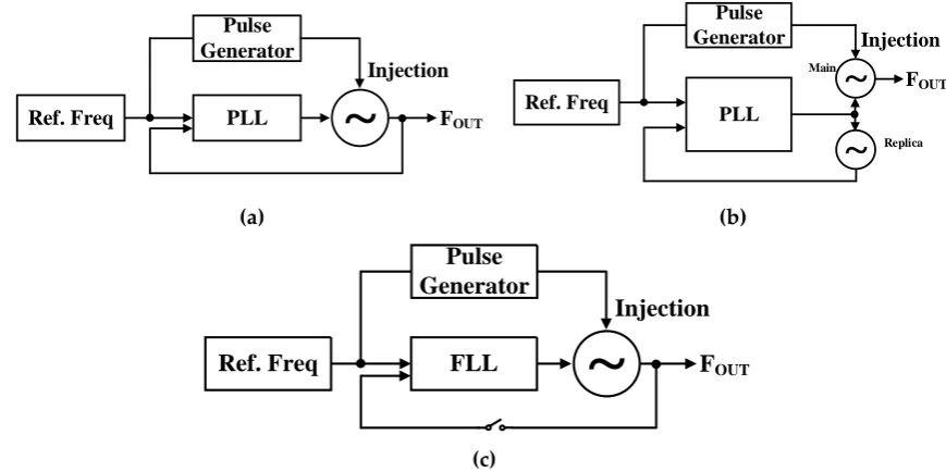
be designed to meet these requirements. The low-IF receiver architectures have become popular for
34
low-power applications. These offer advantages over Zero-IF architecture in terms of the DC-Offset
35
calibration and flicker noise [1]. In Low-IF architecture, the down-converted complex baseband signal
36
is represented by two real I/Q signals. Analog parameter variations in the local oscillators, mixer and
37
filters result in gain and phase errors between I/Q paths. Due to them, image leaks into the signal
38
band during the down conversion process. Therefore, the low-IF receiver has the same low image
39
rejection ratio (IRR) as shown in Figure 1 [2].
40
Methods for solving image problems by compensating I / Q mismatch are presented in [2]-[6].
41
During the I/Q mismatch calibration phase, the Injection-Locked Frequency Multiplier (ILFM) block
42
generates the same frequency as the RF signal before receiving the RF signal through the antenna, as
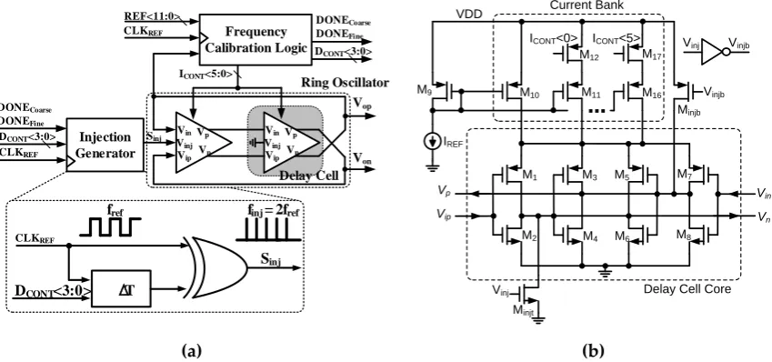
43
shown in Figure 1. Since the low-IF receiver structure crosses the I/Q signal in the band pass filter
44
(BPF), the I/Q mismatch of the BPF input becomes dominant. Therefore, it is effective to add I/QMC
45
(I/Q Mismatch Calibrator) to compensate the mismatch of I/Q signals before BPF. Figure 2 shows a
46
block diagram of the whole low IF using ILFM and I/QMC.
47
48
Figure 1. AC characteristics of low-IF receiver when IQ mismatch occurs.
49
50
Figure 2. The block diagram of Low IF receiver with ILFM.
51
52
A subharmonic ILFM has been considered as a promising solution to generate a low phase noise
53
and high-frequency clocks using limited silicon area and power consumption budget. It injects the
54
reference clock into a Voltage Controlled Oscillator (VCO) and the injection signal realigns the output
55
phase of the free-running VCO so that the low phase noise performance is acquired [7]. This
phase-56
realignment mechanism with the reference clock allows the ILFM to have low jitter performance
57
without a negative feedback system such as a Phase Locked Loop (PLL) or Delay Locked Loop (DLL).
58
However, although the ILFM have many advantages, there is a critical requirement that the good
59
phase noise performance can be achieved only when the target frequency of the ILFM is very close
60
to the free-running frequency of the VCO. Therefore, the good phase noise performance of the ILFM
61
might not be guaranteed, especially for ring oscillators whose free-running frequency is highly
62
sensitive to Process, Voltage, and Temperature (PVT) variation. In addition, if the frequency of the
63
Ring Oscillator is out of the lock range of ILFM due to the PVT variation, ILFM cannot achieve the
64
injection locking [8]. Therefore, ILFM typically requires an effective PVT calibrator or calibration
65
methods to mitigate the sensitivity of performance to the PVT variation.
66
The structure of the conventional and proposed ILFM, as shown Figure 3 [9]. Figure 3(a) shows
67
a conventional ILFM structure with single-loop PLL. The PLL is used to calibrate PVT variation of
68
VCO. However, the structure can’t prevent the real-time frequency drift that is occurred by supply
69
voltage and temperature variations. In addition, the structure has PLL loop path and injection path.
70
It has timing problem because two paths are operated independently [10]. Figure 3(b) shows a
dual-71
loop structure with a main oscillator and a replica oscillator [11]-[16]. The structure is proposed to
72
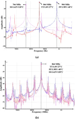
resolve the timing problem of PLL based ILFM. The structure has two VCOs which are main VCO
73
and replica VCO. The replica VCO is not injection lock to prevent the instantaneous frequency drift.
74
Image Frequency
DC FIF
Wanted Frequency
w/ IQ Mismatch
Amplitude
Frequency Interferer
FIF-FInterferer FIF+FInterferer
w/o IQ Mismatch
VGA1
Complex BPF VGA2 Mixer
ILFM ADC
This work
MODEM I
Q
LNA I/Q
MC
I_CAL
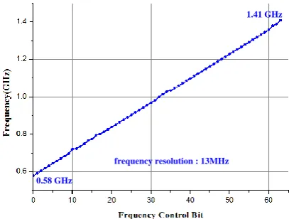
Q_CAL (Q_Mismatch Calibration)
IQ_CAL_MODE RF_MODE
~
~
~
~
~
~
I Path Mismatch
Q Path Mismatch
(I_Mismatch Calibration)
ANT
FILFM
The advantage of this method is that it can be calibrated with a frequency offset and PVT variation
75
of the main VCO in real time using the replica VCO. However, if the mismatch is occurred between
76
main VCO and replica VCO, the structure can’t calibrate PVT variation. Also, the implementation is
77
difficult because it consists of two loops, and there is a disadvantage in that the die area and power
78
consumption are doubled compared to a single structure. Figure 3(c) shows the ILFM structure of an
79
open loop type with Frequency Locked Loop (FLL). Figure 3(c) can reduce the power consumption
80
by turning off the FLL block after FOUT reaches the target frequency using FLL, and the area is small
81
because only a simple FLL circuit is used.
82
(a) (b)
Ref. Freq
FLL
Pulse
Generator
~
Injection
F
OUT (c)Figure 3. Structure of the ILFM (a) PLL based, (b) Dual-loop PLL based, (c) The proposed open-loop
83
ILFM structure using FLL.
84
2. Injection Locked Frequency Multiplier (ILFM) With Frequency Tracking
85
Figure 4(a) shows a block diagram of the proposed ILFM. The proposed ILFM is composed of a
86
Ring Oscillator, an Injection Generator, and FLL. Generally, the clock signal is required for calibration
87
or other purposes in the transceiver or digital block. If the PLL is used to generate clock signal, and
88
this places a burden on this system due to the additional area and power consumption. A Ring
89
Oscillator is proposed instead of the PLL to satisfy the high frequency and low area.
90
The frequency of the Ring Oscillator is generated at close to the target frequency (fTARGET). If the
91
output frequency of the ILFM (fILFM) is near the fTARGET, it is precisely locked to fTARGET by the harmonics
92
of the reference clock frequency (fref), 36 MHz [7].
93
×
ILFM ref
f
= M
f
(1)
94
where fILFM is the output frequency of ILFM, and the multiplication factor M can be changed
95
through the current control of the Delay Cell.
96
Figure 4(b) shows a schematic of the delay cell with an injection switch. The Delay Cell is
97
composed of four inverters, a 6-bit Current Bank, and injection switches. A Ring Oscillator is
98
proposed to acquire fTARGET, as shown in Figure 4(a). The current bank is designed to adjust the
99
frequency using Frequency Calibration Logic. Thus, it is possible to reduce PVT variations and, to
100
reduce phase noise, the injection switches of Minjt, and Minjb are attached to the nodes of Von and Vop,
101
respectively.
102
Figure 5 shows the Frequency Calibration Logic of ILFM. It is composed of a 12-bit Counter, a
103
finite-state machine (FSM), a Digital Comparator, a Coarse Tuning Controller, and a Fine Tuning
104
Controller. Since the ILFM has a locked fTARGET from the Injection Generator, the free running
105
frequency must be close to the fTARGET. Therefore, the role of the Coarse Tuning Controller is to set the
106
frequency close to fTARGET, by calibrating the free running frequency of the Ring Oscillator. The role of
107
Ref. Freq PLL
Pulse Generator
~
InjectionFOUTRef. Freq
PLL Pulse Generator
~
InjectionFOUTMain
the fine tuning controller is to lock the ILFM in a fTARGETby controlling the delay (∆T) the of injection
108
generator. When the frequency calibration logic is started, the 12-bit counter counts the current
109
frequency of the Ring Oscillator. The counted value CNTILFM<11:0> is delivered to the digital
110
comparator.
111
This result, CNTILFM<11:0>, is compared to the reference number, REF<11:0>, which is
112
determined from Eqs. (2) – (3) based on the fTARGET.
113
1
_ (s) = 96
(Hz) CNT ref T EN f (2)
114
= T_EN
CNT(s)
TARGET(Hz)
REF < 11 : 0 >
f
(3)
115
where T_ENCNT is the value of the interval in which the ENCNT signal is High. fref is the reference
116
clock frequency (36 MHz), and fTARGET is the target frequency.
117
(a) (b)
Figure 4.(a) Block diagram of proposed ILFM and (b) schematic of Delay Cell with injection switch.
118
119
Figure 5. Block diagram of the Frequency Calibration Logic.
120
Figure 6(a) shows a flow chart of the Frequency Calibration Logic, and Figure 6(b) is a timing
121
diagram of the FSM in the Frequency Calibration Logic. A 12-bit Counter is used to calculate the
122
output frequency of the ILFM. It operates in an asynchronous way when a counter enable signal
123
(ENCNT) is high and is periodically reset by the counter reset signal (RSTCNT) generated by the FSM.
124
The FSM determines the timing of the calibration by generating the decision clock (CLKTUNE) and a
125
comparison clock (CLKCOMP) using the CLKREF signal [17].
126
ICONT<5:0>
CLKREF Frequency
Calibration Logic
Injection Generator
CLKREF
DCONT<3:0>
DCONT<3:0>
Sinj DONECoarse DONEFine Ring Oscillator fref ΔT
finj= 2fref
Sinj
DCONT<3:0>
REF<11:0> CLKREF Vinj Vin Vip Vp Vn Vop Delay Cell Von Vp Vn Vinj Vin Vip DONECoarse DONEFine M1 Vip M2 M3 M4 M5 M6 M7 M8 Minjb Minjt Vinj Vinjb Vin IREF
∙∙∙
M9 M10 M11 M16
ICONT<0>
VDD
M12
Current Bank
Delay Cell Core M17
ICONT<5> V inj Vinjb
Vp Vn DONEFine DONECoarse FSM Ring Oscillator 12-bit Counter
ICONT<5:0>
ENCNT CLKREF RSTCNT REF<11:0> Injection Generator Sinj Digital Comparator Coarse Tuning Controller UP/DN
CLKTUNE CNTILFM<11:0>
CLKCOMP
Frequency Calibration Logic
Fine Tuning Controller DONECoarse
DONEFine
DCONT<3:0>
Vop (FILFM)
127
(a)
128
129
(b)
130
Figure 6.(a) Flow chart of Frequency Calibration Logic and (b) Timing diagram of 1-state of FSM in
131
Frequency Calibration Logic.
132
If the value of CNTILFM<11:0> is higher than REF<11:0>, the DN is generated by the Coarse Tuning
133
Controller and Fine Tuning Controller. On the other hand, if the value of CNTILFM<11:0> is lower than
134
REF<11:0>, UP is generated. The calibration time is minimized by applying the binary search
135
algorithm. Therefore, ICONT<5:0> is determined by the Coarse Tuning Controller after this loop has
136
been operated 6 times. The fine tuning works in the same way as the coarse tuning, and the DCONT<3:0>
137
values are determined when fine tuning is in progress. The DCONT<3:0> output determines the
138
injection pulse width of the Injection Generator. The output frequency of the Ring Oscillator is
139
sensitive to a PVT corner variation [7].
140
Figure 7(a) shows the simulation result of the frequency variation of the ILFM that is changed
141
by the PVT variation. When Frequency Calibration Logic is not used, the output frequency of the
142
ILFM changes from 766 MHz to 948 MHz depending on the corner condition.
143
NO Set ILFM "ICONT<5:0>,
DCONT<3:0>"initial value
Counting "FILFM"
for a set period time
"DN" Decrease Frequency (ICONT<N> = '0')
YES
Coarse Lock Done, Fine Calibration Start
"UP" Increase Frequency (ICONT<N> = '1')
YES All bit of
"ICONT<5:0>"
is determined?
"CNTILFM<11:0>" > "REF<11:0>"?
NO
Coarse Calibration Start
NO Counting "FILFM"
for a set period time
"DN" Decrease Frequency (DCONT<n> = '0')
YES
"UP" Increase Frequency (DCONT<n> = '1')
All bit of
"DCONT<3:0>"
is determined? N←N-1
Calibration Ended Determine "ICONT<5:0>,
DCONT<3:0>"
NO
n←n-1
"CNTILFM<11:0>" > "REF<11:0>"?
ICONT<5> is determined.
ICONT<N> is determined.
CLKREF (36MHz)
ENCNT
CLKCOMP
CLKTUNE
RSTCNT
27.77ns
T_ENCNT(=2.66us)
ICONT<0> is determined.
On the other hand, Figure 7(b) shows the simulation result when the proposed Frequency
144
Calibration Logic is used, and the output frequency of ILFM is exactly calibrated to target frequency
145
(846 MHz) at all PVT corner conditions.
146
147
(a)
148
149
(b)
150
Figure 7. The frequency of ILFM Frequency Calibration (a) before calibration and (b) after calibration.
151
3. Experimental Results
152
Figure 8 shows a chip microphotograph of the ILFM. The proposed design is fabricated in a 0.18
153
μm CMOS process and the area of the ILFM is 0.54 mm × 0.12 mm.
154
155
Figure 8. Chip microphotograph of ILFM
156
864 MHz TT/1.8V/27°C
Frequency (Hz)
A
m
p
li
tu
d
e
(d
B
)
984 MHz FF/1.98V/-40°C 766 MHz
SS/1.62V/120°C
-20
-40
-60
-80
-100
700M 800M 900M 1G
Frequency (MHz)
A
m
p
li
tu
d
e
(d
B
)
864 MHz
TT/1.8V/27°C
FF/1.98V/-40°C
SS/1.62V/120°C
-10
-20
-30
-40
-50
-60
-70
-80
700M 800M 900M 1G
0
.1
2
m
m
Figure 9 is the ILFM top transient simulation result. As shown in the flow chart in Figure 8, find
157
the target frequency while performing the FLL operation. After both the DONECoarse and DONEFine
158
signals change to 'H', the CLKREF signal is injected and injection locked to the target frequency.
159
160
Figure 9. The top simulation of ILFM
161
Figure 10 shows the measurement results of the free-running frequency of the Ring Oscillator.
162
The frequency of the Ring Oscillator can be adjusted in units of about 13 MHz and has a frequency
163
range from 0.58 GHz to 1.41 GHz.
164
Figure 11 shows the measured injection locked full range of ILFM. The measured Injection lock
165
range is form 612 MHz to 1152 MHz. After the Frequency Calibration operation, the ILFM can lock
166
to N times the reference clock within the Injection Locked range.
167
168
Figure 10. Free-running frequency range of Ring Oscillator.
169
170
Figure 11. Injection Locked frequency range of ILFM.
171
Time (us) Coarse Tuning Fine Tuning Injection Lock
36MHz Clock
CLKREF
Vop
ENCNT
RSTCNT
FILFM
15.96us 29.26us
933 MHz
762 MHz 849 MHz891 MHz
871 MHz
860 MHz 864 MHz
DONECoarse DONEFine
1.41 GHz
0.58 GHz
frequency resolution : 13MHz
612 MHz ILFM Freq. Min
864 MHz ILFM Freq. Center
Figure 12 shows the measured phase noise of the injection locked in ILFM. When the short pulse
172
is injected into the Ring Oscillator, the phase noise is -108 dBc/Hz at 1 MHz offset. When the ILFM is
173
locked by injection, the phase noise is reduced more than the free-running noise. With the effect of
174
the injection, in-band phase noise is also reduced.
175
176
177
Figure 12. Measurement of injection locked phase noise at center frequency.
178
Table I shows the comparison with published papers ([18]-[20]). The proposed paper is designed
179
to make an RF signal to the RF frontend before the RF signal is input from the antenna. RF signals for
180
calibrating I / Q mismatch do not require ultra-low jitter performance. The reference spur is generated
181
by the ILFM, and it is attenuated by the BaseBand Filter. The performance of the proposed paper with
182
the highest priority is the silicon area and current consumption. The definition of FOM is defined as
183
follows:
184
2
10 log
1 1
RMS diss
Jitter P
FoM
s mW
(4)
185
where Jitterrms, 1s, and Pdiss are the RMS jitter value of ILFM output, 1 second, the power
186
consumption, respectively [20].
187
Table 1. Performance Comparison of ILFM
188
[18] [19] [20] This work
Process (nm) 180 nm 65 nm 65 nm 180 nm
Topology IL+ Open
Loop IL+ DPLL IL+ DPLL IL+ FLL
Output Frequency (GHz) 1.88 0.576-0.608 2.5-5.75 0.612–1.152
Reference Frequency (MHz) 80 32 125 36
Phase noise
(dBc/Hz @1MHz offset) -122 -114 -115.9 -108
Jitterrms (ps)
(Integ. Range) N/A
4.23 (100 Hz ~ 40MHz)
0.34 (10 kHz ~ 40MHz)
6.3 (1kHz ~40MHz)
Power consumption (mW) 55 10.5 5.3 0.95
Active area (mm2) 0.31 0.158 0.158 0.0648
FoM (dB) N/A -217 -242.4 -194.2
4. Conclusions
189
This paper presents a 612-1152 MHz Injection Locked Frequency Multiplier (ILFM). The
190
proposed ILFM is only used for sending an input signal to the receiver in the I/Q mismatch calibration
191
mode. Using the Phase-Locked Loop (PLL) to calibrate the receiver places a burden on this system
192
due to the extra area required and power consumption. Instead of the PLL, to satisfy high frequency,
193
low jitter, and low area, a Ring Oscillator is proposed. The free-running frequency of the ILFM is
194
automatically digitally calibrated to reflect the frequency of the injected signal from the harmonics of
195
the reference clock. To control the frequency of the ILFM, the load current is digitally tuned with
6-196
bit digital control signal. The proposed ILFM locks to the target frequency using a digitally controlled
197
Frequency Locked Loop (FLL). This chip is fabricated using 1-poly 6-metal 0.18 µ m CMOS and
198
achieve the wide tuning range of 612~1152 MHz. The power consumption is 0.95 mW from a supply
199
voltage of 1.8 V. The measured phase noise of the ILFM is -108 dBc/Hz at a 1 MHz offset.
200
Acknowledgments: This work was supported by the Technology Innovation Program (10076507) funded By the
201
Ministry of Trade, Industry & Energy(MOTIE, Korea)
202
Author Contributions: Kang-Yoon Lee guided and directed the authors for this work. SungJin Kim and
Dong-203
Gyu Kim studied, proposed and designed the overall architecture of Open Loop ILFM with FLL. They wrote the
204
paper. Chanho Kim, Dongsoo Lee and Sang-Sun Yoo contributed in making the layout of the proposed
205
architecture. Keum Cheol Hwang guided the antenna and measurments. Young Gun Pu performed the
206
measurements with SungJin Kim, Dong-Gyu Kim and Chanho Kim. Youngoo Yang and Minjae Lee designed
207
the related top architecture.
208
References
209
1. Salamin, Y.; Pan, J.; Wang, Z.; Tang, S.; Wang, J.; Li, C.; Ran, L. Eliminating the Impacts of Flicker Noise
210
and DC Offset in Zero-IF Architecture Pulse Compression Radars. IEEE Trans. Microw. Theory and Techn.,
211
vol 62, no. 4, April 2014.
212
2. Lerstaveesin, S.; Song, B. A complex image rejection circuit with sign detection only. IEEE J. Solid-State
213
Circuits, vol 41, no. 12, pp. 2693-2702, Dec. 2006.
214
3. Mahattanakul, J. The effect of I/Q imbalance and complex filter component mismatch in low-IF receivers.
215
IEEE Trans. Circuits Syst. I, Exp. Briefs, Reg. Papers, vol 53, no 2, pp. 247-253, Feb. 2006.
216
4. Kim, S.Y.; Jeong, M.S.; Kim, Y.G.; Kim B.K.; Lee, T.J.; Lee, K.H.; Kim, B.E. A complex band-pass filter for
217
low-IF conversion DAB/T-DMB tuner with I/Q mismatch calibration. in Proc. IEEE ASSCC, 2008, pp.
473-218
476.
219
5. Xu, Y.; Chi, B. Power-scalable, complex bandpass/low-pass filter with I/Q imbalance calibration for a
220
multimode GNSS receiver. IEEE Trans. Circuits Syst. II, Exp. Briefs, vo. 59, no. 1, pp. 30-34, Jan. 2012.
221
6. Kitsunezuka, M.; Tokairin, T.; Maeda, T.; Fukaishi, M. A low-IF/zero-IF reconfigurable analog baseband IC
222
with an I/Q imbalance cancellation scheme. IEEE J. Solid-State Circuits, vol. 46, no. 3, pp. 572-582, Mar. 2011.
223
7. Choi, S.; Yoo, S.; Choi, J. A 185fsrms-Integrated-Jitter and -245dB FOM PVT-Robust Ring-VCO-Based
224
Injection-Locked Clock Multiplier with a Continuous Frequency-Tracking Loop Using a Replica-Delay Cell
225
and a Dual-Edge Phase Detector. in IEEE Int. Solid-State Circuits Conf. (ISSCC) Dig. Tech. Papers, Feb.
226
2016, pp. 192-193.
227
8. Kim, M.; Choi, S.; Seong, T.; Choi, J. A Low-Jitter and Fractional-Resolution Injection-Locked Clock
228
Multiplier Using a DLL-Based Real-Time PVT Calibrator With Replica-Delay Cells. IEEE J. Solid-State
229
Circuits, vol. 51, no. 2, Feb. 2016.
230
9. Bae, W. "Frequency acquisition technique for injection-locked clock generator using
asynchronous-231
sampling frequency detection," in Electronics Letters, vol. 53, no. 18, pp. 1240-1242, 8 31 2017.
232
10. Coombs, D.; Elkholy, A.; Nandwana, R.K.; Elmallah, A.; Hanumolu, P.K. 8.6 A 2.5-to-5.75GHz 5mW
233
0.3psrms-jitter cascaded ring-based digital injection-locked clock multiplier in 65nm CMOS. in Proc. IEEE
234
Int. Solid-State Circuits Conf. (ISSCC) Dig. Tech. Papers, 2017, pp. 90-91
235
11. Musa, W.; Deng, T.; Siriburanon, M.; Miyahara, K.; Okada, Matsuzawa, A. A compact, power and
low-236
jitter dual-loop injection locked PLL using all-digital PVT calibration. IEEE J. Solid-State Circuits, vol. 49, no.
237
1, pp. 50-60, Jan. 2014.
238
12. Deng, W.; Yang, D.; Ueno, T.; Siriburanon, T.; Kondo, S.; Okada, K.; Matsuzawa, A. A 0.0066 mm2 780 μW
239
fully synthesizable PLL with a current-output DAC and an interpolative phase-coupled oscillator using
edge-injection technique. in IEEE Int. Solid-State Circuits Conf. (ISSCC) Dig. Tech. Papers, Feb. 2014, pp.
241
266-267.
242
13. Deng, W.; Musa, A.; Siriburanon, T.; Miyahara, M.; Okada, K.; Matsuzawa, A. A 0.022 mm2 970 μW
243
injection-locked PLL with -243 dB FOM using synthesizable all-digital PVT calibration circuits,” in IEEE
244
Int. Solid-State Circuits Conf. (ISSCC) Dig. Tech. Papers, Feb. 2013, pp. 248-249.
245
14. Deng, W.; Yang, D.; Ueno, T.; Siriburanon, T.; Kondo, S.; Okada, K.; Matsuzawa, A. A fully synthesizable
246
all-digital PLL with interpolative phase coupled oscillator, current-output DAC, and fine-resolution digital
247
varactor using gated edge injection technique. IEEE J. Solid-State Circuits, vol. 50, no. 1, pp. 68-80, Jan. 2015.
248
15. Lee, Y.; Kim, M.; Seong, T.; Choi, J. A low phase noise injection locked programmable reference clock
249
multiplier with a two-phase PVT calibrator for ΣΔ PLLs. IEEE Trans. Circuits Syst. I Reg. Papers, vol. 62,
250
no. 3, pp. 635-644, Mar. 2015.
251
16. Lee, J.; Wang, H. Study of Sub-Harmonically Injection- Locked PLLs,” IEEE J. Solid-State Circuits, vol. 44,
252
no. 5, pp. 1539-1553, May 2009.
253
17. Lee, D.S.; Jang, J.H.; Park, H.G.; Hwang, K.C.; Yang, Y.G.; Seo, M.K.; Lee, K.Y. A Wide-Locking-Range Dual
254
Injection-Locked Frequency Divider with an Automatic Frequency Calibration Loop in 65-nm CMOS. IEEE
255
Trans. Circuits Syst. II, Exp. Briefs, vol. 62, no. 4, pp. 327-331, Apr. 2015.
256
18. Kobayashi, Y.; Amakawa, S.; Ishihara, N.; Masu, K. A low-phase-noise injection-locked differential
ring-257
VCO with half-integral subharmonic locking in 0.18 μm CMOS,” in Proc. IEEE ESSCIRC, 2009., Sep. 2009
258
pp.440-443.
259
19. Park, P.; Park, J.; Park, H.; Cho, S. An all-digital clock generator using a fractionally injection-locked
260
oscillator in 65 nm CMOS. in IEEE Int. Solid-State Circuits Conf. (ISSCC) Dig. Tech. Papers, Feb. 2012
261
pp.336-337.
262
20. Elkholy, A.; Talegaonkar, M.; Anand, T.; Hanumolu, P.K. Design and Analysis of Low-Power
High-263
Frequency Robust Sub-Harmonic Injection-Locked Clock Multipliers. IEEE J. Solid-State Circuits, 2015, pp.
264
3160-3174
265
21. Liang, C.; Hsiao, K. An Injection-Locked Ring PLL with Self-Aligned Injection Window. in Proc. IEEE Int.
266
Solid-State Circuits Conf. (ISSCC) Dig. Tech. Papers, 2011, pp. 90-91
267
22. Choi, S.; Yoo, S.; Lim, Y.; Choi, J. A PVT-Robust and Low-Jitter Ring-VCO-Based Injection-Locked Clock
268
Multiplier with a Continuous Frequency-Tracking Loop Using a Replica-Delay Cell and a Dual-Edge Phase
269
Detector. IEEE J. Solid-State Circuits, 2016, pp. 1878-1889