http://www.sciencepublishinggroup.com/j/ajmsp doi: 10.11648/j.ajmsp.20190401.17
ISSN: 2575-2154 (Print); ISSN: 2575-1530 (Online)
Development of a Simplistic Method to Simulate the
Formation of Intermetallic Compounds in Diffusion
Soldering Process
Chironjeet Chaki
1, *, Manoshi Chaki
2, Keya Roy
31Department of Mechanical Engineering, Rajshahi University of Engineering & Technology, Rajshahi, Bangladesh 2
Department of Apparel Engineering, Bangladesh University of Textiles, Dhaka, Bangladesh 3
Department of Civil Engineering, Rajshahi University of Engineering & Technology, Rajshahi, Bangladesh
Email address:
*
Corresponding author
To cite this article:
Chironjeet Chaki, Manoshi Chaki, Keya Roy. Development of a Simplistic Method to Simulate the Formation of Intermetallic Compounds in Diffusion Soldering Process. American Journal of Materials Synthesis and Processing. Vol. 4, No. 1, 2019, pp. 54-61.
doi: 10.11648/j.ajmsp.20190401.17
Received: May 30, 2019; Accepted: July 2, 2019; Published: July 15, 2019
Abstract:
A simplistic simulation technique has been developed for computing the individual intermetallic compound (IMC) thickness which is formed in substrate-solder (Cu-Sn) systems during the diffusion soldering process in high-temperature power electronic applications. The method requires the time-dependent temperature profile for the soldering process and the growth rate parameters (e.g. concentration gradient, diffusion coefficient, activation energy, etc.) for the development of IMC layers as input. The method is suitable for predicting the thickness of an intermetallic phase layer during the diffusion soldering process. As such, it can be used in high-temperature power electronic application’s solder processing to enhance the reliability and lifetime of solder interconnections by allowing the control of the thickness of IMC layers. The method is demonstrated for IMC growth between pure copper as substrate and pure Sn as solder material. The growth behavior of the IMC layer is increased with increasing temperature over time according to the Arrhenius theory in the temperature range between 24°C to 260°C. To simulate the formation of IMC thickness in diffusion soldering interconnections, a simplistic way has been attempted using the popular commercial finite element simulation tool Comsol Multiphysics and scientific computing application ‘Matlab’. By means of transient thermal input, the diffusion-controlled intermetallic phase formation is simulated here. Few assumptions are taken care of this simulation process, for example, no convection, no reaction, solid-solid diffusion, no the pressure effect on the computational domain.Keywords:
Diffusion Soldering, Finite Element Model, Power Electronic Application, Interconnection Technology1. Introduction
Among all the interconnection technologies soldering still is the predominant technique for high-temperature power electronics applications. In the soldering process of Cu-Sn system, the Cu (Substrate) is diffused into liquid solder (Sn) which results in the nucleation of intermetallic compounds in the bulk of the solder material. During that time, molten solders (Sn) react with Substrate (Cu) films to form Cu6Sn5
(ƞ) and Cu3Sn (ε) intermetallic compounds, after which the
solder joints are established. These layers grow fairly rapidly during the diffusion soldering process. At the early stage of
the reactions, the Cu6Sn5 phase with a monoclinic structure
formed first, followed by the appearance of the orthorhombic Cu3Sn phase. The morphology of Cu6Sn5 IMC appears like
scallops, while that of Cu3Sn is layer-type. The diffusivities of
Cu in Cu6Sn5 and Cu3Sn IMCs are much less than those in
molten solders. It is reported that the Cu6Sn5 IMC is the
dominant phase during transient liquid phase soldering at temperatures below 260°C. Only after the solder is completely consumed, the Cu3Sn layer starts to grow thicker.
solder joint, the resulting thickness of the layer is of particular importance to the integrity of a joint and, thus, to the reliability of the electronic device. In standard electronics, only thin layers of intermetallic compounds are realized for good solder connections because thick growth of intermetallic compounds leads to faster crack propagation in layer and failure of connection. But for high-temperature applications in power electronics, to avoid the problems with low-melting Sn-Cu based solders, a relatively more solder layer (Sn) between the chip and direct copper bonded (DCB) is to be transformed into intermetallic compounds as they have better thermal stability. In addition to this, intermetallic compounds are inherently hard and brittle and, therefore, have a low fracture toughness. The objective of this research work to develop a simplistic numerical method for calculating the thickness of an intermetallic layer formed in solder/substrate systems during the solder joint fabrication is introduced.
2. Available Methods
2.1. Phase Field Method
Phase-field method which solves the interfacial problems. At the interfacial region, it replaces the boundary conditions by a partial differential equation to evaluate a secondary field. Recently, the phase field formulations have been used to simulate soldering reactions. [2] In each of phases, the filed considers two different values (for example +1 and -1). At the interfacial region, it allows horizontal changes between both values, afterward, which can diffuse [3] with a finite width. It is one of the useful methods to simulate the evolution of microstructural.
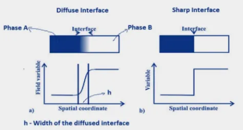
In the phase field simulation, the microstructures are composed of different size of grains. The shape and common circulation of the grains is represented by the functions called phase field variables which are continuous in space and time. The below figure (1) Illustrates the interfacial region where the diffused interface is shown in figure (1-a) and the sharp interface is shown in figure (1-b) including the indication of different phases. The width h is also indicated in the figure which creates the difference between diffused and sharp interface.
Figure 1. Illustration of (a) diffusion and (b) sharp interface.
Within the grains, where the values of phase field variables
have remained constant, which are relevant to the structure, positioning, and conformation of the grains. Grain size valuation or the interface positioning as a function of time is implicitly provided by the development of the phase field variables.
The temporal evolution is depicted by a number of differential conditions, which are possibly solved by different numerical methods.
In phase field model, the free energy function, composition constraint with the condition of local thermodynamic equilibrium, multiphase field function of time in term of relaxation equation and diffusion in respect of mass flux equation is to be defined [2]. The total free energy function is defined by the below equation (1).
∑ ∑ · ∑ (1)
Where fi is chemical free energy density in phase i, ci is the
phase composition, ԑij is the gradient energy coefficient and
ωij represents the potential energy barrier between two phase
ϕi and ϕj. In the phase-field modeling, the evolution of
multiphase fields [4] as a function of time follows the following relaxation equation (2).
!∑ χ χ "
# #
$ (2)
Where Np is the number of coexisting phases, Mij
represents the mobility of the interfacial region. The derivative of total free energy F with respect to ϕi and ϕj is
defined in the below equation (3).
# ∑
%
$ (3)
For mass diffusion, the mass flux equation is set with respect to diffusion coefficient, free energy density and composition gradient for the multiphase system. The transformation of the flux equation into the diffusion equation is conceivable by using the spatial differentiation with diffusivity which fluctuates as a function of phase fields. The following equation (4) is given as the diffusion equation.
% · & ∑
'( (4)
2.2. Monte Carlo Simulation Method
To solve the magnetic domain problem, Potts and Ising models have been used widely and Monte-Carlo grain growth simulation begins from that model. The Potts model permits multiple states namely Q states for individual particles in the entire system, on the other hand, Ising model comprises two spin states called up and down. For Modeling and simulation of material characteristics, for instance, the texture evolution and grain growth simulation, the Potts model has widely been used by several researchers.
each lattice location, an integer number between Q and 1 is assigned for initializing the lattice. In the system domain, Q denotes the total number of orientations. Two neighboring locations with dissimilar grain arrangement numbers are observed as being disconnected by a grain boundary and individual pair of different adjoining locations contributes a piece of grain boundary energy to the whole system. A collection of grain location having a similar arrangement number and bounded by grain boundaries are considered as a grain. The complete energy of the entire system is computed by the below equation (5) which is related to the grain boundary energy contributions through all the grain locations.
) * ∑0 +1 -. . / (5)
Where, summation of i is the overall Monte-Carlo locations in the system, the totaling of j is overall nearest neighbor locations of the site i, and δij is the Kronecker delta. This
method simulates the grain development iteratively.
2.3. Multiscale Simulation Method
The combination of the Monte-Carol simulation method and the Finite Element method is called the Multiscale simulation which simulates the growth of intermetallic compounds by means of microstructural evaluation. The method is developed under the principle which says the stored energy of solder material is increased steadily throughout the each thermal cycle. The recrystallization is begun when an energy critical value is introduced. New grain growth and the nucleation are achieved by releasing the stored energy which consumes the strain hardened matrix of high dislocation density gradually. For modeling the macroscale in homogenous deformation, the finite element method is used in this particular simulation. On the other hand, modeling the mesoscale microstructural evolution Monte-Carlo simulation model is applied. A correlation between the Monte-Carlo simulation time and the real time is recognized while comparing with the in-situ experimental result. The effects of intermetallic phases (for example Cu3Sn and Cu6Sn5) on
recrystallization in the solder matrix are also been encompassed in the multiscale simulation. [4, 7]
2.4. Dual Phase Lag Model
The dual phase lag model was originally developed for the diffusion medium to compute the formation of the interfacial compounds in thin films and metal matrix composites. The kinetics of interfacial phase formation in Multiscale simulation model and solder interconnections also applied the Dual phase lag model to demonstrating the intermetallic phase growth in solder joints, e.g. intermetallic growth in a pure Sn-Cu system at 170°C. Some researchers have further applied this model to simulate the growth of the interfacial intermetallic phase for the Sn-3.5Ag (solder) & Cu (substrate) and Sn-3.5Ag-0.7Cu (solder) & Cu (substrate) systems during the reflow soldering. The Dual Phase Lag model also be used to describe some of the singularities of the intermetallic phase formation in solder interconnections, however, it provides
only a 1-D simulation model in nature. [8]
3. Model Development
3.1. Choosing the Equation of the Physics
During intermetallic formation, inter-diffusion which is driven by the atomic concentration gradient can be described by the second Fick’s law. In COMSOL Multiphysics, the Transport of Diluted Species module is used to compute the concentration field. Transport and reactions of the species dissolved in a gas, liquid, or solid can be computed in this module. As described above, the reaction is assumed to be zero. So the transport of diluted species module is arranged according to the assumption mentioned above.
The COMSOL model with Transport of diluted species module follows the generic diffusion equation which has the same structure as the heat conduction equation and is governed by the following mass transfer equation (6). As the convection is assumed to be zero, the equation (6) is prepared according to the assumption.
1 2 &23 4
(6)
Where G is the reaction rate. For the simplicity of the model, the reaction rate will be assumed to be zero here (G=0), then the equation (6) would be in below form of equation (7).
1 2 &23 0
(7)
Equation (12) is the governing transport equation for the diffusion soldering process. Where D is the growth rate constant which is equivalent to diffusivity if intermetallic compound formation is diffusion controlled. Here in this study, it has been assumed that the TLP soldering is diffusion controlled. According to the Arrhenius equation (8) as below, the diffusivity is determined by the activation energy Q (KJ/mol), the diffusion coefficient Do (m2/s), and the absolute temperature T (K).
& &6789 + ;<:/ (8)
Where R (J/(mol×K) is the universal molar gas constant. The universal gas is actually composed by Boltzmann constant and Avogadro's Constant. So the value of R can be calculated by multiply Boltzmann constant with Avogadro's constant where the Boltzmann constant = 1.38064852 × 10⁻²³ m2 kg s-2 K-1 and Avogadro's Constant = 6.02214086 × 10²³ mol-1.
3.2. Model Setup
The steps are taken to set up the simulation model is given below: (a) Geometry setup and Material selection (b) Meshing (c) Boundary conditions (d) Running the simulation.
3.3. Geometry Setup
2D geometry was considered as a part of preparing the simulation model to see the concentration gradient due to the diffusional variation. In the geometry, the top and bottom domain are selected as tin (Sn) and copper (Cu) respectively. The length/width of both Sn and Cu is selected as 5 mm, on the other hand, the height/thickness of both Sn and Cu is 40 µm.
Figure 2. Geometry of Cu-Sn system with dimensions.
Material data plays an important role in finite element simulation. [9] Pure Tin (Sn) and Copper (Cu) was selected to simulate the intermetallic phase formation in this research work. In the real application some other soldering materials are used but in most of the tin (Sn) based solder alloy where the rest of the composition percentage is less than 3%.
3.4. Meshing
In order to analyze the concentration gradients, computational domains are splitted into smaller subdomains. The governing equations are then discretized and solved inside each of these subdomains. For this work, finite element method (FEM) was used to solve the approximate version of the system of equations where quadrilaterals mesh was chosen for the computational domain.
To mesh the model, the user-defined mesh parameter option was selected in COMSOL and meshed according to the maximum element size. The maximum element size
determines the minimum number of nodes for the model. The more important factor for the transient model is the maximum time stepping size for the model. As a time-dependent COMSOL model, the maximum time stepping size determines the smoothness and accuracy of the data. There are three types of meshing with different element size according to the computational domain was tested. All are given below with the number of elements, element size and element ratio according to the X and Y axis of the computational domain. All three types of meshing are illustrated graphically with geometrical setup in the below figure 3. Meshing parameter such as the number of mesh element, element size, and ratio are explicitly shown in table 1 which are examined later.
Figure 3. Meshing representation of the geometry with type 1, 2 and 3 mesh elements.
Table 1. Meshing parameter according to X and Y axis.
Mesh
Parameter Y-axis
Type 1 Type 2 Type 3
X-axis (Cu) X-axis (Sn) X-axis (Cu) X-axis (Sn) X-axis (Cu) X-axis (Sn)
Number of Element 100 20 20 40 40 20 40
Element size (µm) 50 2 2 1 1 2 1
Element ratio 0 1 1 1 1 1 0.5
After testing the different meshing, type 3 was implemented in the current simulation model. Type 3 mesh gives better convergence in the result because it has optimum element size in the computational domain.
3.5. Boundary Condition
Initially, 100% Cu and 0% Sn was selected in the left computational domain. On the other hand, 100% Sn and 0% Cu was selected in the right computational domain. No flux boundary condition was implemented at the edge of the domain. One of the important input is at the interface between two media. At the boundary, two conditions are specified. A condition that links the dependent variable in the two regions and a condition that links the flux of the dependent variable in each region. For this simulation, it was assumed that the continuity of the flux across the boundary and the dependent variable.
parameters are listed with their names, value, unit and the relevant description. [11, 12] Table 2 represents the parameter used in the current simulation process. Those important parameters are imported into the COMSOL computational module which are the necessary constants and variables to simulate the concentration gradient of Cu-Sn system.
Table 2. Necessary parameter for COMSOL module.
Parameter Value Unit Description
Cu_Do 2.4×10⁻⁷ m2/s Diffusion coefficient of Cu
Sn_Do 2.95×10⁻⁹ m2/s Diffusion coefficient of Sn
Cu_Q 60 KJ/mol Activation energy of Cu Sn_Q 53 KJ/mol Activation energy of Sn R 8.314 J/(mol×K) Universal gas constant t_start 0 s Starting time of simulation t_end 1098 s Ending time of simulation
t_step 1 s Time step
3.6. Importing Temperature Profile as a Global Function
After setting all the parameters, COMSOL imports MATLAB generated temperature profile as a global function. An interpolated function is used in current time-dependent study. An interpolated function can create a smooth function which allows the dependent variable is plotted against the independent variable. [13] Matlab script generates transient thermal input which I call it here as temperature profile. In the profile, Cu-Sn system is heated from initial temperature to a peak temperature with a certain heating gradient. Then it is heated at constant peak temperature for some time which is called as handling time (th). After that, the system is cooled
down to the room temperature with a cooling gradient. In this research work, the initial/ room temperature (Ti) is selected as
24°C. Peak temperature (Tp) is selected as 260°C. The heating
(∆H) and cooling (∆C) gradients vary from 0.5 K/s. The
handling time (th) vary from 1.5 minutes to 30 minutes. The
temperature profile is shown in the below figure 4.
Figure 4. Time-dependent temperature profile which is imported as transient thermal input into COMSOL computational module.
3.7. Setting the Diffusion Coefficient as Variable
As the soldering process is depending on diffusion between solder and substrate, the concentration changes in the Cu-Sn system also depends on the diffusion coefficient. As the diffusion coefficient is temperature dependent [14], it changes with temperature in every time steps. So, both Sn and Cu were
taken as a global variable which changes in every time step during the simulation.
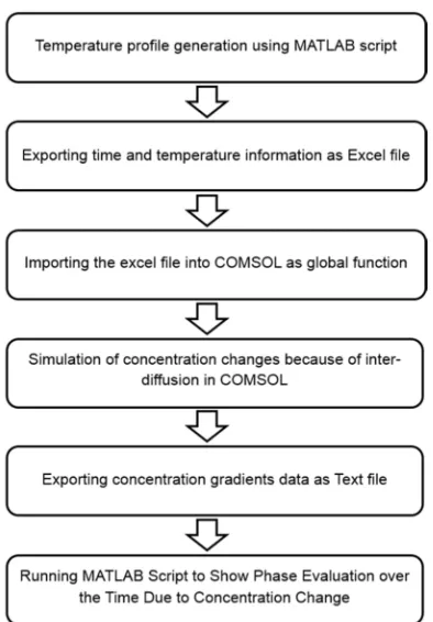
3.8. Simulation Process Overview
A MATLAB script was written to show the output of Cu-Sn from COMSOL in terms of concentration gradients and reforms the result in Intermetallic phase thickness. Figure 5 shows the flow chart of visualizing individual intermetallic phase recognition and formation during the simulation. The total simulation process is divided into six stages which is graphically represented in figure 6. In the beginning, a MATLAB script generates the user-defined temperature profile. After defining the inputs, COMSOL import it as a global variable where temperature changes over time. After importing the temperature inputs into COMSOL, necessary other variables and constants are defined. Subsequently, COMSOL simulates the concentration gradient using finite element method. For simulating the concentration gradients, transport of dilute species (tds) module was used in COMSOL which represents the mass transportation equation due to diffusion. The simulation output contains the information of concentration in every location of the computational domain over time. Finally, a MATLAB script was used to show the intermetallic phase formation. The MATLAB script reads the simulation file and based on the composition of two important intermetallic phases (Cu6Sn5 and Cu3Sn), an atomic
concentration range was arranged which defines the phase formation of two intermetallic compounds as well as pure Cu and Sn. An algorithm is defined in MATLAB to show the concentration change of every phase in every time steps which is shown in figure 5.
Figure 5. Flow chart of visualizing results for each intermetallic compounds in terms of phase thickness.
Figure 6. Overview of the simulation process for intermetallic compounds growth behavior.
4. Results
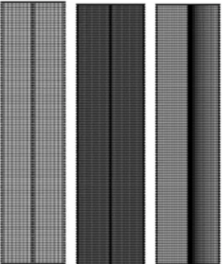
4.1. Evolution of Intermetallic Phases
The direct output from the simulation is the atomic concentration of Cu-Sn system with respect to the location and time. In the below figure shows four individual phase formation over time. In the beginning, there was 100% Sn in the right side and 100% Cu on the left side. But over time two more phase forms due to diffusion. It is commonly known that Cu and Sn react with each other at the interface [15] to form an intermetallic compound of Cu6Sn5 and Cu3Sn. The
intermetallic Cu6Sn5 forms very fast and grows with
scallop-like morphology because Cu atoms diffuse inside Sn through fast atomic transport phenomena. Atomic concentration profile can be plotted along the perpendicular direction of IMC interface at any time points by this way the determination of total IMC thickness is possible.
In the early stages of the diffusion process, Cu atoms dissolved into the molten Sn and form Cu6Sn5 intermetallic
compounds at the room temperature because Cu atoms diffuse faster in Sn which is shown in Figure 7. After that Cu6Sn5
reacts with Cu and form Cu3Sn IMC. [6] Figure 7 shows how
the different phases are evolved over time. The reaction kinetics are given below.
6Cu + 5Sn = Cu6Sn5
Cu6Sn5 + 9Cu = Cu3Sn
Figure 7. Concentration changes over the time for (a) th =0 min (b) th =10
min (c) th =10 min.
4.2. Case Study
Table 3 describes all the parameter of the simulation study. In this case study both the heating (∆H) and cooling (∆C)
gradients are kept as constant where the value of both gradients remains 2.5 K/s. The peak temperature is selected as 260°C in this particular study. The initial/room temperature is selected as 24°C. A variant is added here which is handling time (th) that varies from 1.5 minutes to 30 minutes. The
maximum time of the simulation or total time of a study is calculated as 33 minutes at handling time of 30 minutes and the peak temperature of 260°C.
Table 3. Constant heating and cooling gradients with varying handling time at a peak temperature of 260°C.
Heating Gradient (K/s) Handling time (th) Cooling Gradient (K/s)
2.5 1.5 2.5
2.5 5 2.5
2.5 10 2.5
2.5 15 2.5
2.5 20 2.5
2.5 25 2.5
2.5 30 2.5
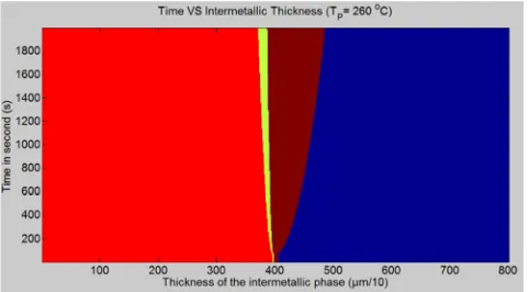
The dimension of the geometry (computation domain) is kept as same (Cu=40µm, Sn=40µm) in the entire case study of this simulation work. All the assumptions are the same as described at the beginning. The intermetallic phase evolution over time is graphically represented in figure 8 and 9.
Figure 8. The evolution of Intermetallic phase thickness over the time period at a peak temperature of 260oC while t
Figure 9. The evolution of Intermetallic phase thickness over the time period at a peak temperature of 260oC while t
h=5 min.
Figure 8 and 9 represents how the intermetallic phases (Cu6Sn5 and Cu3Sn) change over time. In the figure, Y-axis
denotes the time in second and X-axis denotes the phase thickness in µm (µm/10 in scale). The light red color (left side) represents the substrate (Cu) and blue color (right side) represents the pure solder material (Sn). In between two of them, another two colors are grown from bottom to top and those are two intermetallic phases. The bigger percentage or the dark red color (on the side of Sn) is Cu6Sn5 and lower
percentage or green color (on the side of Cu) is Cu3Sn. This
graphic is prepared using Matlab. Basically, both of the figures have been captured from real-time animation during the simulation while data was exchanging simultaneously between COMSOL and Matlab.
Figure 10 shows that intermetallic phase thickness of Cu6Sn5 and Cu3Sn at the peak temperature of Tp = 260°C
having different handling time while the heating and cooling gradients are constant (∆H = ∆C = 2.5 K/s). The handling time
varies from 1.5 minutes to 30 minutes where the maximum intermetallic thickness of Cu6Sn5 and Cu3Sn observed as 9.9
µm and 1.6 µm at handling time of th= 30 minutes. From
figure 8, it is shown that the intermetallic compound growth of Cu6Sn5 is higher than Cu3Sn which is actually seen in
experiments. [16] Normally Cu6Sn5 start to form in the room
temperature when Sn (solder) and Cu (substrate) react together. On the other hand, Cu3Sn need more time to form
even more temperature. So after a certain temperature Cu3Sn
start to form and grow more with increasing handling time.
Figure 10. IMC Thickness growth over handling time (th) at Tp= 260°C with
fixed ∆H = ∆C = 2.5 K/s.
5. Conclusion
In this research work, a simplistic simulation method was attempted to develop by which we can predict the intermetallic compounds formation in diffusion soldering process [17] in the solder-substrate interface as well as the thickness of those phases with a specific time-dependent temperature profile. For the simplicity of the design of the simulation method, solder and substrate material is chosen as pure tin (Sn) and copper (Cu) in this study. Two particular intermetallic compounds such as Cu6Sn5 and Cu3Sn were described here which is grown during the diffusion soldering process of Cu-Sn system. The total simulation process was divided into three sub-process. At the first step, a MATLAB script was used to generate the time-dependent on the temperature profile. After that popular CAE tool called COMSOL Multiphysics simulated the concentration gradient of the system during the diffusion process between Cu and Sn where the temperature profile was the input function in the COMSOL global definition area. The diffusion coefficient was also taken as a variable where the depending variable was temperature. Finally, a MATLAB script was written to illustrate the intermetallic phase formation over the time period based on the result of concentration gradients from COMSOL. For simulating the concentration gradients, transport of dilute species (tds) module was used inside the COMSOL module which represents the mass transportation equation due to diffusion. The maximum thickness of the intermetallic phases was observed at peak temperature, Tp= 260°C, heating and cooling gradient, ∆H = ∆C = 2.5 K/s and
the handling time, th= 30 minutes where the thickness of
Cu6Sn5 and Cu3Sn were calculated as 9.90 µm and 1.60 µm
respectively.
References
[1] C. F. Dickinson and G. R. Heal, “Solid–liquid diffusion controlled rate equations”, Thermochimica Acta, vol. 340–341, pp. 89–103, 1999.
[2] M. S. Park and R. Arróyave, “Computational investigation of intermetallic compounds (Cu 6Sn5 and Cu3Sn) growth during solid-state aging process”, Computational Materials Science, vol. 50, no. 5, pp. 1692–1700, 2011.
[3] A. Staroselsky, R. Acharya, and B. Cassenti, “Phase field modeling of fracture and crack growth”, Engineering Fracture Mechanics, vol. 205, no. October 2018, pp. 268– 284, 2019.
[4] T. Min, Y. Gao, L. Chen, Q. Kang, and W. Q. Tao, “Mesoscale investigation of reaction-diffusion and structure evolution during Fe-Al inhibition layer formation in hot-dip galvanizing”, International Journal of Heat and Mass Transfer, vol. 92, pp. 370–380, 2016.
[6] W. L. Chiu, C. M. Liu, Y. S. Haung, and C. Chen, “Formation of plate-like channels in Cu6Sn5and Cu3Sn intermetallic compounds during transient liquid reaction of Cu/Sn/Cu structures”, Materials Letters (Elsevier), vol. 164, pp. 5–8, 2016.
[7] H. Ma, A. Kunwar, J. Sun, B. Guo, and H. Ma, “In situ study on the increase of intermetallic compound thickness at anode of molten tin due to electromigration of copper”, Scripta Materialia (Elsevier), vol. 107, pp. 88–91, 2015.
[8] Z. Huang, P. P. Conway, and R. Qin, “Modeling of interfacial intermetallic compounds in the application of very fine lead-free solder interconnections”, Microsystem Technologies, vol. 15, no. 1 SPEC. ISS., pp. 101–107, 2009.
[9] R. Turner, F. Schroeder, R. M. Ward, and J. W. Brooks, “The importance of materials data and modelling parameters in an FE simulation of linear friction welding”, Advances in Materials Science and Engineering, vol. 2014, pp. 1–9, 2014. [10] E. G. Flekkøy, R. Delgado-Buscalioni, and P. V. Coveney,
“Flux boundary conditions in particle simulations”, Physical Review E - Statistical, Nonlinear, and Soft Matter Physics, vol. 72, no. 2, pp. 1–9, 2005.
[11] J. F. Li, P. A. Agyakwa, and C. M. Johnson, “A numerical method to determine interdiffusion coefficients of Cu6Sn5 and Cu3Sn intermetallic compounds”, Intermetallics (Elsevier), vol. 40, pp. 50–59, 2013.
[12] B. Chao, S. H. Chae, X. Zhang, K. H. Lu, J. Im, and P. S. Ho, “Investigation of diffusion and electromigration parameters for Cu-Sn intermetallic compounds in Pb-free solders using simulated annealing”, Acta Materialia, vol. 55, no. 8, pp. 2805–2814, 2007.
[13] M. Wizard and G. Definitions, “Introduction to COMSOL Multiphysics,” pp. 1–6, 2014.
[14] A. Morozov, A. Freidin, W. H. Müller, A. Semencha, and M. Tribunskiy, “Modeling temperature dependent chemical reaction of intermetallic compound growth”, 20th International Conference on Thermal, Mechanical and Multi-Physics Simulation and Experiments in Microelectronics and Microsystems (EuroSimE), 2019, pp. 1–8.
[15] Y. Tang, Q. W. Guo, S. M. Luo, et al., “Formation and growth of interfacial intermetallics in Sn-0.3Ag-0.7Cu-xCeO2/Cu solder joints during the reflow process”, Journal of Alloys and Compounds (Elsevier), vol. 778, pp. 741–755, Mar. 2019. [16] C. Chaki, M. Chaki, and K. Roy, “Formation of Intermetallic
Compounds in Diffusion Soldering Joints in High Temperature Power Electronic Applications”, International journal of innovative research in technology, vol. 5, no. 11, pp. 724–732, 2019.