Design of High Speed Approximate Multiplier
with Carry Speculation Compressor
Anju Sunny Binu K. Mathew
PG Student Associate Professor
Department of Electronics & Communication Engineering Department of Electronics & Communication Engineering Saintgits College of Engineering Saintgits College of Engineering
Dhanusha P. B Assistant Professor
Department of Electronics & Communication Engineering Saintgits College of Engineering
Abstract
Approximate computing is an important paradigm for digital processing. Most computer arithmetic applications are implemented using digital logic circuits, thus operating with a high degree of reliability and precision. However, many applications such as in multimedia and image processing can tolerate errors and imprecision in computation and still produce meaningful and useful results. Accurate and precise models and algorithms are not always suitable for efficient for use in these applications. Multiplication using speculation/prediction has higher speed compared to conventional multipliers. They are quite effective interns of power dissipation when high speed is required
Keywords: Almost Correct Adder, Approximate Multiplier, Speculation, Three Dimensional Reduction, Vertical Compressor Slice
________________________________________________________________________________________________________
I.
I
NTRODUCTIONMost computer arithmetic applications are implemented using digital logic circuits, thus operates with a high reliability and precision. However, many applications such as, multimedia and image processing can tolerate errors and imprecision in computation and still produce meaningful and useful results. The paradigm of inexact computation relies on relaxing fully precise and completely deterministic building modules for designing energy-efficient systems. In digital designs, integer multiplication is one of the fundamental building blocks, which affects the microprocessor and DSP performance. Fast non-booth multipliers mostly use well known schemes such as Wallace, Dadda or the Three-Dimensional Method (TDM). These are all based on a carry-save compression tree, which utilizes full adders and half adders to turn a multi operand sum to two operand addition, which is further realized by using a final carry-propagate adder. In this paper we have considered an approximate multiplier which uses a speculative functional unit.
II.
L
ITERATURE REVIEWSpeculative Functional Unit (SFU): A.
SFUs aim to achieve delay improvements, at the same time introducing less power and area overheads. SFUs can predict carry of one or more cells used in the design and hence reduce the critical path length along the entire array of cells. Predictors proposed for these SFU designs are very much similar to branch predictors employed in microprocessors. Predicting a carry involve deciding whether the bit value will be “1” or “0,” similar to prediction of the outcomes of branches. SFUs however yield significant decrease in the critical path of an arithmetic unit. For instance, in the previous works it has been shown that for a linear adder structure and an array-based multiplier, the reduction is by 50% and 25%, respectively. Also, it can be noted that the carry bit prediction used in a SFUs is different from methods used in adder circuits to probabilistically determine the value of the carry. These methods use additional combinational logic to the existing functional unit inputs for determing the value of the current carry. SFUs can be constructed for both adders and multipliers.
Multiplication: B.
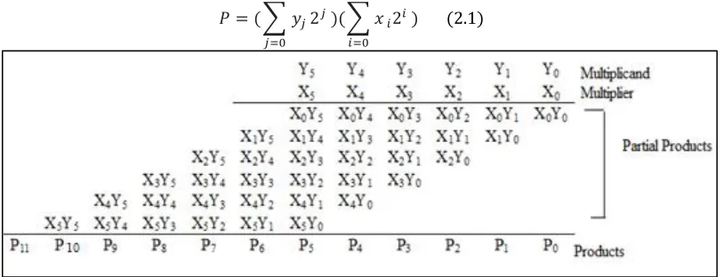
A M × N-bit multiplication P = Y × X can be viewed as forming N partial products of M bits each, and then summing the appropriately shifted partial products to produce an M+ N-bit result P. Binary multiplication is equivalent to a logical AND operation. Therefore, generating partial products consists of logical ANDing of the appropriate bits of the multiplier and multiplicand. Each column of partial products must then be added and, if necessary, any carry values passed to the next column. We denote the multiplicand by the equation Y = {yM–1, yM–2… y1, y0} and the multiplier as X = {xN–1, xN–2… x1, x0}. For unsigned multiplication, the product is given in equation below.
∑
∑
Fig. 1: Partial Products (“CMOS VLSI Design” By Weste And Harris)
A fast multiplier usually comprises of three parts or modules: Partial product generation, a Carry Save Adder (CSA) tree to reduce the partial products’ matrix to sum of only two operands and a Carry Propagation Adder (CPA) for the final computation of the binary output.
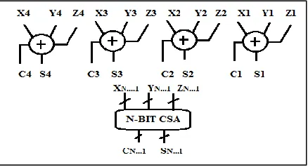
Carry save Adder (CSA): C.
A number of techniques are available to perform multiplication, but the choice is depended on factors like latency, power, speed, area, throughput, design complexity, energy. Fast multipliers utilize CSA (Carry Save Adders) adders to sum the partial products. A CSA has a delay of 1.2-2FO4 inverters independent of the width of the partial product, whereas a carry propagate adder has 4-15+FO4 inverter delay depending on width, architecture and circuit family ((“CMOS VLSI Design by Weste and Harris”)).
Fig. 2: CSA (“CMOS VLSI Design” By Weste And Harris)
Existence of Fast Inputs and Fast Outputs: D.
The delay from an input to an output in a full adder is not the same. This delay is dependent on a particular transition (0-to-1, 1-to-0). Therefore it is also possible to come up with different realizations of a full adder wherein a specific signal path is favoured with respect to the others and has been designed in such a way that a signal propagation of this path takes a minimal amount of time. This is sometimes done even at the expense of all other possible signal paths. In the case of a ripple carry adder, (“Oklobdzija et. al. 1996”)it is designed so that the carry in to carry-out delay is minimized.
In that respect consider particular implementation of a (3, 2) counter as shown in the figure given below. In the case of a parallel multiplier, the design objective is to minimize the delay from the Inputsto the Sum, of the Full Adder which has direct effect on the critical path. The delay from input Aor B to the Sum is equal to two equivalent XOR delays. The delay for the path from Cin to output Sum is equal to one XOR equivalent delay. We define Cin as a fast input. For this case, the propagation delay from A or B to the output Sum is twice as long as the propagation delays from input Cin to the Sum output. Considering the delay at the output Sum, in this particular technology delay from input A or B to Sum output is equivalent to two XOR delays. However, delay from inputs (A, B, or Cin) to the output Carry is equivalent to one XOR delay. We define Carry as a fast output. The value of those delays varies with technology and particular circuit implementation. In general we can use any (non- integer) values in our algorithm.
Fig. 3: Signal Delays In Full Adder (“Oklobdzija Et. Al. 1996”)
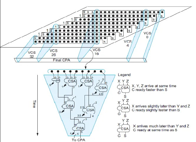
Three Dimensional Reduction Method (TDM): E.
Instead of developing an efficient compressor structure and then using it for partial product reduction, we consider a global approach. Here the compressor consists of a vertical slice where partial product array is represented in space and time. The vertical cross-section slice in fig.2.4 represents partial product compressor of the multiplier array. The vertical slice is further interleaved with compressors that are utilized in the reduction process. This is referred to as Vertical Compressor Slice (VCS) (“Oklobdzija et. al. 1996”). There are number of input signals into the vertical slice and number of output signals originating from the particular VCS which are passed to next VCS corresponding to the first higher order bit position. By considering just one VCS, we can see how the matrix of partial products is reduced by a tree of counters. However every full adder employed produces an output carry which affects the slice of superior weight. Hence critical path is not only a vertical path through a given slice but also a horizontal path through the slice. The goal of this scheme is to minimize both path delays by building VCS slice optimized to have minimal delay.
(“CMOS VLSI Design, Weste and Harris”). A half adder is assumed to have half the delay. Horizontal carries are indicated by diagonal lines coming from behind the slice or pointing out of the slice. VCS16 receives five horizontal carries from VCS15 and generate six horizontal carries to VCS17. The final carryout is shifted by one column before feeding to the CPA. The inputs to the CSA are arranged based on their arrival times to reduce the multiplier delay. The reduction of partial products bits in this scheme is performed by creating a bit slice compressor whose size is equal to size of a given vertical cross-section of the partial product matrix and then it is assembled in to an integral structure as shown in fig.2.5. Since VCS is optimized by considerin g neighboring VCS as well as their signals are taken in to account. The optimization is a three-dimensional optimization process.
Fig. 4: VCS In TDM Multiplier (“CMOS VLSI Design” By Weste And Harris)
Fig. 5: PPM Divided Into VCS Slices (“Oklobdzija Et. Al. 1996”)
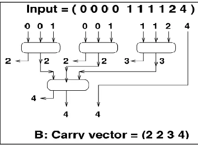
Three Greedy Approach: F.
A heuristic for TDM design is proposed that we will call the three-greedy approach. The three-greedy approach is as follows: Take for the inputs of each gate gi the three smallest values in Ii-1. For example, the adder circuit shown in Fig. 2.6 is three-greedy. Gate g1 is given by g1 = (0, 0, 0) takes as its inputs the three smallest values in I0 = I = (0, 0, 0, 0, 1, 1, 1, 1, 2, 4), and generates a sum bit at time 2. Thus, I1 = (0, 1, 1, 1, 1, 2, 2, 4), and we build gate g2 = (0, 1, 1). Similarly, we can say I2 = (1, 1, 2, 2, 3, 4), g3 = (1, 1, 2), I3 = (2, 3, 3, 4), g4 = (2, 3, 3), and therefore Vs = (4, 5). Also, we can see VC = (1, 2, 3, and 4). Note that the three-greedy strategy produces undominated circuits, since the three-greedy approach produces the lexicographically smallest carry vector, but it may be possible to produce circuits with better sum delays and/or incomparable carry vectors using other strategies.
Fig. 6: Three Greedy Approach (“Stelling Et.Al. 1998”)
Two Greedy Approach: G.
The two-greedy strategy, which is defined as follows, gate gi is always constructed using the two smallest values in Ii-1 plus a third value in Ii-1. The key fact we prove is that, for any column circuit C (I), there exists a two-greedy column circuit C (I) that dominates C (I). Thus, in searching for optimal combinations of column circuits, we can restrict our attention to two-greedy circuits
.
Fig. 7: Two Greedy Approach (“Stelling Et.Al. 1998”)
III.
P
ROPOSED MULTIPLIER ARCHITECTUREIn this project, a high speed approximate multiplier has been designed. The multiplier delay has been reduced by optimizing the TDM carry save tree used in the multiplier design.
Speculative Multiplier Architecture: A.
In the equation 2.1, the computation of P requires the summation of partial products xiyj according to their weights 2 i+j
are independent and equally likely. As a result the probability of being one for each partial product is 0.25. Fig3.2 shows the partial product matrix of a 16x16 multiplier. As it can be seen that, the leftmost and rightmost column of the partial product matrixcomprise a small number of partial products, whereas the inner columns are higher. The delay will obviously be related to the height of the PPM: higher the matrix, higher the multipliers delay. In principle, the delay can be reduced by deleting some partial products from the inner columns of the Partial Product Matrix (PPM).
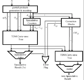
Fig. 8: Architecture of Approximate Multiplier with Carry Speculation Compressor (“Cilardo Et. Al 2014”)
However the probability each product is 0.25 and the deletion of each term will increase the error probability of this naïve approach. Here the speculative carry-save reduction tree is based on three steps: partial products recoding, partial products partitioning, speculative compression.
Fig. 9: Initial PPM (“Cilardo Et. Al 2014”)
Partial Products Recoding: B.
Consider two partial products aibj and ajbi of the i+j-th column of the PPM. Now we define two modified partial products: Ai, j = aibj AND ajbi (3.1)
Oi, j = aibj OR ajbi (3.2)
original partial product (i.e. 0.25). Alternatively the probability of Oi, j is 7/16. From the above two observations it can be concluded that speculative carry tree utilizes lower probability terms, to minimize the probability of misprediction.
Fig. 10: PPM After Recoding (“Cilardo Et. Al 2014”)
Partial Products Partitioning: C.
Only the lower probability terms Ai, j is included in the speculative carry-save tree. Partial products belonging to the largest columns of PPM are only recoded. The partial products in the columns 11, 12……22 are recoded.
Speculative Compression: D.
Although the probability Ai, j has been reduced with respect to the original partial products, simple deletion of Ai, j terms would introduce a very large misprediction probability. Thus, instead of deleting the terms we sum them in an approximate manner by using speculative compressors.
A (m: 2) speculative counter is defined as a component with m inputs (x0……..xm-1) and two outputs sum S and Carry C. The value (2C+S) is equal to the arithmetic sum of inputs when not more than three inputs are high. The output S is obtained by xor ing the inputs. The calculation of the carry (C) signal poses certain difficulties. Let f ≥2(x0……..xm-1) be the binary function which is high when any two input signals are high. The function given by, f ≥2(x0……..xm-1) correspond to the carry signal. In case of two inputs it is given by:
f ≥2(x0,.x1) = x0 * .x1 (3.3)
Similarly when there are three inputs f ≥2, correspond to the carry signal of a full adder given by, f ≥2(x0,.x1, x2) = x0 * .x1 + x1 * x2 + x0 * x2 (3.4)
When the number of inputs increases, say m ≥ 5, we may use a divide and conquer approach to compute the carry signal. The five inputs are divided two disjoint sub sets i.e, the first subset includes x0, .x1 and x2 and the second subset include x3 and x4. Then the carry signal is given by:
f ≥2(x0,.x1, x2, x3, x4) = f ≥2(x0,.x1, x2) + f ≥2(x3, x4) + f ≥2(x0 +x1 + x2, x3, x4) (3.5)
Equation 3.5 can be implemented using the circuit given below. This modified full adder circuit computes carry output as f ≥2(x0,.x1, x2) and the sum outputs as the OR between x0,.x1, x2. Similarly the modified half adder computes the carry output as f ≥2(x3, x4) and the sum outputs as the or between x3 and x4.
Correction Block: E.
The correction circuits are not very critical module for overall multiplier. The error signal is ORed to generate error output. This is outside the critical path. The function realizes by the error correction block can be described using half adders and full adders. For example a (4:2) correction circuit must produce a single bit error word EW with weight 2; it is high only if all the inputs are 1.
Fig. 12: (5: 2) Error Correction Block (“Cilardo Et. Al 2014”)
The complete architecture of the proposed speculative multiplier is outlined in fig. 3.1. The multiplier inputs are firstly processed by the partial products generation and recoding block. This block computes all the partial products aibj and recodes Oi, j those belonging to the inner columns of the PPM, generating and recoded partial products. The terms Ai, j is processed by the speculative counters obtaining the reduced Si, j and Ci, j terms. The obtained Si, j and Ci, j terms and the un-recoded aibj and the recoded Oi, j partial products are summed together by using a TDM carry-save tree. The TDM considers the different arrival times of its inputs and tries to make proper connections to full adders so that the delay throughout each path is approximately the same. Thus, the late arriving outputs of the speculative counters are connected to the shortest delay path in the TDM. Globally, at the TDM outputs we obtain a delay profile similar to the one of a conventional multiplier. The maximum delay, however, is reduced compared to conventional multipliers, owing to the use of speculative counters and ACA. The two outputs of the TDM tree are added by using a speculative adder, obtaining the speculative result. Since each of the speculative compressors used in the multiplier can introduce an error, a correction block is needed for each speculative compressor.
The correction block receives the same inputs as that of speculative compressor and generates two outputs: an error flag E is said to be high, if four or more inputs to the speculative compressor are “1”. The error correction word is constructed in such a manner that, so that by the addition of EW to the speculative compressor output (2C+S) so that correct result is obtained.
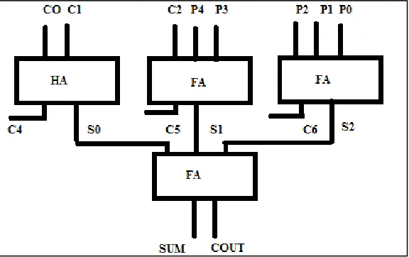
The error flag produced by each of the respective correction blocks are OR-ed and OR-ed with the error flag of the speculative adder to obtain the error signal of the speculative multiplier. In case of error the non-speculative result is computed by summing the error correction EW with the outputs of TDM carry save tree and in the final adder used is a fast non speculative adder like CLA. The figure below shows a TDM carry save tree with eight inputs which includes five partial products(p0, p1, p2, p3, p4) and three intermediate carry (c0, c1, c2) from the previous vertical compressor slice.
Fig. 13: TDM with Eight Inputs
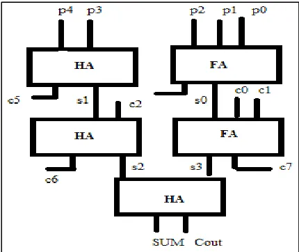
Optimised TDM Design: F.
Fig. 14: Optimized TDM Tree With Eight Inputs
For instance in the above example where TDM is fed with five inputs which includes five partial products (p0, p1, p2, p3, p4) and three intermediate carry (c0, c1, c2) from the previous vertical compressor slice, TDM design is modified to reduce the delay. Since co, c1, c2 are generated after one unit delay they are fed in the manner shown above.
IV.
R
ESULTS AND DISCUSSIONThe multiplier with and without optimized TDM design have been simulated and synthesized using ISE design suite 14.5
Simulation Waveform of Multiplier without Optimised TDM: A.
The simulated waveform of multiplier without optimised TDM is shown in fig. 4.1
Fig. 15: Simulation Waveform Of Approximate Multiplier Without Optimised TDM
Simulation Waveform of Multiplier with Optimised TDM: B.
The simulated waveform of multiplier with optimised TDM is shown in fig. 4.2
Fig. 16: Simulation Waveform Of Approximate Multiplier With Optimised TDM
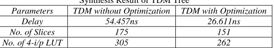
Both the approximate designs have been simulated and synthesized separately and output has been obtained. It is found that the multiplier employing optimized TDM has lesser delay as compared to the TDM tree before optimization and in both the designs the error percentage is found to very small.
The results can be tabulated as in table 4.1 and 4.2.
Table - 4.1
Synthesis Result Of Multiplier Without Optimized TDM
Parameters Speculative Multiplier without Optimization Speculative Multiplier with Optimization
Table - 4.2 Synthesis Result of TDM Tree
Parameters TDM without Optimization TDM with Optimization
Delay 54.457ns 26.611ns
No. of Slices 175 151
No. of 4-i/p LUT 305 262
V.
C
ONCLUSIONApproximate computing is particularly interesting for multimedia designs. These designs depend on different features of compression, as in here imprecise computation. In- exact computation has the advantage of decreasing the number of transistors, delay, and power consumption as compared to the exact designs. In this paper we have come up with an approximate multiplier design. The circuit utilizes some of the partial product as well as a speculative compression tree to sum the recoded partial products. A speculative adder is used in the final carry propagate addition.
The multiplier design is further optimized to have small delay by proper allocation of the intermediate carry that are generated in the vertical compression slice of the TDM tree. The designs functionality have been verified using Xilinx ISE design suite 14.5 (web-edition). The approximate multipliers are useful in critical application, justifying the more complex architecture. In cases where multiplier speed is not critical, the use of speculative units remains unjustified. The performance of the approximate multiplier can further be improved by considering don’t care conditions and further by using variable latency adder instead of almost correct adder.
R
EFERENCES[1] L. S. Wallace, “A suggestion for fast multipliers,” IEEE Trans.Comput., vol. EC-13, pp. 14–17, Feb. 1964.
[2] L. Dadda, “Some schemes for parallel multipliers,” Alta Frequenza, vol. 34, Mar. 1965
[3] V. G. Oklobdzija, D. Villeger, and S. S. Liu, “A method for speed optimized partial product reduction and generation of fast parallel multipliers using an
algorithmic approach,” IEEE Trans. Comput., vol. 45, no. 3, pp. 294–306, Mar. 1996.
[4] P. F. Stelling, C. U. Martel, V. G. Oklobdzija, and R. Ravi, “Optimal circuits far parallel multipliers,” IEEE Trans. Comput., vol. 47, no. 3, pp. 273–285,
Mar. 1998.
[5] J. Umand T. Kim, “An optimal allocation of carry-save-adders in arithmetic circuits,” IEEE Trans. Comput., vol. 50, no. 3, pp. 215 233, Mar. 2001.
[6] T. Liu and S. L. Lu, “Performance improvement with circuit-level speculation,” in Proc. 33rd Annu. IEEE/ACMInt. Symp.Microarchit. 2000, pp. 348–355.
[7] S. L. Lu, “Speeding up processing with approximation circuits,” Computer, vol. 37, no. 3, pp. 67–73, Mar. 2004.
[8] A. A. Del Barrio, S. O. Memik, M. C. Molina, J.M.Mendias, and R. Hermida, “A distributed controller for managing speculative functional units in high
level synthesis,” IEEE Trans. Comput.-Aided Design Integr. Circuits Syst., vol. 30, no. 3, pp. 350–363, Mar. 2011.
[9] A. A. Del Barrio, R. Hermida, J. M. Mendías, M. C. Molina, and S. O. Memik, “Multispeculative additive trees in high-level synthesis,” in Proc. Design,
Autom., Test Eur. Conf. (DATE), 2013.
[10] A. K. Verma, P. Brisk, and P. Ienne, “Variable latency speculative addition: A new paradigm for arithmetic circuit design,” in Proc. Design, Autom, Test
Eur. (DATE), Mar. 2008.
[11] A. Cilardo, “A new speculative addition architecture suitable for two’s complement operations,” in Proc. Design, Autom, Test Eur. Conf. Exhib. (DATE),
Apr. 2009, pp. 664–669.
[12] K. Du, P. Varman, and K.Mohanram, “High performance reliable variable latency carry select addition,” in Proc. Design, Autom, Test Eur.Conf. Exhib.
(DATE), 2012.
[13] A. A. Del Barrio, R. Hermida, S. O. Memik, J. M. Mendıas, and M. C. Molina, “Multispeculative addition applied to datapath synthesis,” IEEE Trans. Comput.-Aided Design Integr. Circuits Syst., vol. 31, no. 12, pp. 1817–1830, Dec. 2012.
[14] S. Ghosh, D. Mohapatra, G. Karakonstantis, and K. Roy, “Voltage scalable high-speed robust hybrid arithmetic units using adaptive clocking,” IEEE Trans.
Very Large Scale Integr. (VLSI) Syst., vol. 18, pp. 1301–1309, Sep. 2010.
[15] A. K. Verma and P. Ienne, “Improving XOR-dominated circuits by exploiting dependencies between operands,” in Proc. Asia South Pacific Design Autom.
Conf., 2007, pp. 601–608.
[16] S. F. Hsiao, M. R. Jiang, and J. S. Yeh, “Design of high-speed low power 3-2 counter and 4-2 compressor for fast multipliers,” Electron. Lett., vol. 34, no.
4, pp. 341–343, 1998
[17] C. H. Chang, J. Gu, and M. Zhang, “Ultra low-voltage low-power CMOS 4-2 and 5-2 compressors for fast arithmetic circuits,” IEEE Trans. Circuits Syst. I,
Reg. Papers, vol. 51, no. 10, pp. 1985–1997, Oct. 2004.
[18] S. Veeramachaneni, K. Krishna, L. Avinash, S. Puppala, and M. B. Srinivas, “Novel architectures for high-speed and low-power 3-2, 4-2 and 5-2
compressors,” in Proc. 20th IEEE/ACM Int. Conf. VLSI Design (VLSID 2007), Jan. 2007.
[19] P. Song and G.DeMicheli, “Circuit and architecture trade-offs for high speed multiplication,” IEEE J. Solid-State Circuits, vol. 26, no. 9, pp. 1184–1198,
Sep. 1991.
[20] A. G. M. Strollo, N. Petra, and D. De Caro, “Dual-tree error compensation for high performance fixed-width multipliers,” IEEE Trans. Circuits Syst. II,
Exp. Briefs, vol. 52, no. 8, pp. 501–507, Aug. 2005.
[21] N. Petra, D. De Caro, V. Garofalo, E. Napoli, and A. G. M. Strollo, “Truncated binary multipliers with variable correction and minimum mean square error,” IEEE Trans. Circuits Syst. I, Reg. Papers, vol. 57, no. 6, pp. 1312–1325, Jun. 2010.
[22] N. Petra, D. De Caro, V. Garofalo, E. Napoli, and A. G. M. Strollo, “Design of fixed-width multipliers with linear compensation function,” IEEE Trans.
Circuits Syst. I, Reg. Papers, vol. 58, no. 5, pp. 947–960, May 2011.
[23] D. De Caro, N. Petra, A. G. M. Strollo, F. Tessitore, and E. Napoli, “Fixed-width multipliers and multipliers-accumulators with min max approximation
error,” IEEE Trans. Circuits Syst. I, Reg. Papers, vol. 60, no. 9, pp. 2375–2388, Sep. 2013.
[24] J. M. Hammersley and D. C. Handscomb, Monte Carlo Methods. London, U.K.: Methuen, 1964.
[25] M. H. Kalos and P. A. Whitlock, Monte Carlo Methods, 2nd ed. Weinheim, Germany: Wiley-VCH, Oct. 2008