DESIGN OF A VERIFICATION TECHNIQUE FOR
QUADRATURE PHASE SHIFT KEYING USING
MODEL SIM SIMULATOR FOR BROADCAST
COMMUNICATION RELEVANCE’S
Thota Markandeyulu
1, S.Siva Sankar Reddy
21
M.Tech (VLSI) Scholar,
2Asst. Professor (ECE)
Nalanda Institute of Engg and Tech. (NIET), Siddharth Nagar, Guntur, A.P, (India)
ABSTRACT
This article presents the design of modulator for Quadrature phase shift keying (QPSK). QPSK also one type of
phase shift keying which is under the digital modulation. The digital modulation is more efficient in
transmission and more secure compared to other. The noise detection and correction are better in digital
techniques over analog techniques. Convert the input data in digital and transfer over analog channel is defined
the digital modulation. In these days, main factor to be considered is low power and less time. Shift keying
techniques defines as the carrier bit stream changes in one or more parameters depending on the input bit
stream, which we need to send. This present technique is designed in Verilog HDL and synthesized on XILINX
ISE tool.
Keywords
: Quadrature Amplitude Modulation, Amplitude Phase Shift Keying, Binary Phase Shift
Keying.
I. INTRODUCTION
Digital techniques have replaced analog techniques in present growing world. Modulation is the process of
changing the carrier signal. Digital modulation is defined as the processing of digital data transmission from
transmitter to receiver over the analog informational channel (medium). In this process of modulation, the
message signal changes the parameters of carrier signal. Usually we consider that amplitude, frequency and
phase are the parameters for any signal or sequence. The digital modulation is classified depending on the basis
of parameters of carrier signal. In digital modulation, three different techniques have present. These are:
1. Amplitude shift keying
2. Frequency shift keying
3. Phase shift keying
In digital technique, changing in the phase of the carrier is defined as Phase Shift Keying. The digital
modulators are required to generate these signals depending on the technique we need. QPSK principle is often
used in phase shift keying modulators. Both the accuracy and the stability of the generated signals must
generally be addressed in the main factors of accuracy and stability. In real time, these are particularly when the
This digital transmission system has proved that it is more efficient than analog transmission because of the
advancements in the fields of Digital Signal Processing (DSP) and Very Large Scale Integration (VLSI). In
digital transmission, noise immunity, multiplexing different forms of information, security has improved and
advantage over analog transmission. Phase shift keying uses a finite number of phases unlike all other digital
modulation techniques, which uses finite number of distinct signals to represent the data.
II. LITERATURE SURVEY
2.1 Quadrature Amplitude Modulation
For high speed digital signals the dominant modulation mechanism is this QAM. This QAM becomes our daily
usage system as wireless protocols, modems to military for personal communications. In QAM, the two carriers
are of 90 degrees out of phase and makes change in the amplitude of the carrier signals.
Implementation of QAM has done in three stages i.e., modulation, transmission and demodulation. In this article,
we are focusing on modulation itself. The modulation involves two stages:
1. Serial to parallel conversion
2. Digital to analog conversion
In serial to parallel conversion, it changes the bit stream into log2M streams, where M is number of symbols.
The bit rate is defined as 1/log 2M.
In second digital to analog conversion, the input streams have index a look up table. One signal modulates
quadrature Q, carrier and the other modulates in-phase I, carrier. Sampling rate of the system is greater than the
symbol rate then it is called analog. Here we can’t fine true analog system. Finally add Q and I signal to form a
QAM signal.
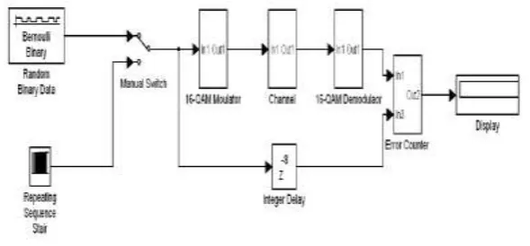
Fig 1: Example Diagram For 16-QAM
2.2 Binary Phase Shift Keying
BPSK also called as phase reversal keying (PRK) or two phase shift keying. It is simplest form of PSK. It takes
two phases separated by 180 degrees. That’s the reason why generally it is called as 2-PSK. We can’t say where
these points have located. It has many disadvantages like the highest rate of noise distortion, can able to transmit
1 bit/symbol. So, it is not suitable for high data transmission applications.
In BPSK, the term “binary” is indicating that it can transfer one binary valued quantity within bit duration.
Phase shifting made by π. Keying comes back to the first electrical communication system. It is a method of
transferring the message on carrier. That carrier signal may be base band signals or free- space transmissions
degrees. BPSK is popular in digital electronics and because of the immunity of noise makes demand in many
fields.
Fig 2: BPSK Modulator
The above figure shows the BPSK modulator. The output of the modulator is defined as
X(t) = I(t) + jQ(t)
III. PROPOSED METHOD
3.1 Quadrature Phase Shift Keying (QPSK)
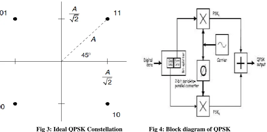
Fig 3: Ideal QPSK Constellation Fig 4: Block diagram of QPSK
QPSK is one of the types of phase shift keying. It is related with the BPSK. This scheme also uses double side
band carrier suppression method as like BPSK but the difference is it can able to send two bits of digital stream
at a time. This makes more amount of users can able to access on the channel.
The generation of QPSK is shown in fig 4. The input data is directly given to the bit splitter to split it as even
(i.e., 0, 2, 4....) and odd (1, 3, 5...) bits. These even bits are directly multiplied with the carrier signal in the
multiplier block to generate a BPSK signal i.e., PSKI as shown in figure. At the same time remaining odd bits
are multiplied with the 90 degrees phase shifted carrier signal in the other multiplier block to generate another
BPSK signal i.e., PSKQ. Then the both BPSK signal simply added in adder block and transmits to output.
I cos ωct + Q sin ωct = R cos (ωct + ѳ)
Where R =
and
Ѳ = tan-1(Q/I).
The modulated signal is defined as simple as
X(t) =I (t) + Q(t).
There the complex signal X(t) is formed by using in-phase component as real part and Quadrature component as
imaginary part. Now we are going to discuss about constellation part.
3.2 Constellation
There are four possibilities for transmission i.e., 00, 01, 10 and 11. At every possibility the modulator shifts the
phase of carrier signal i.e., π/4, 3π/4, 5π/4 and 7π /4 as shown in fig 3. Each output differs by one bit only.
Hence, it is called as 4 PSK. QPSK has to maintain the data rate either double of BPSK data rate while maintain
the bandwidth of the signal or at the time of half bandwidth needed, it uses same data rate of BPSK. QPSK
results in two functions; these are in-phase component and Quadrature component of the signal.
3.3 Flow Chart for QPSK Process
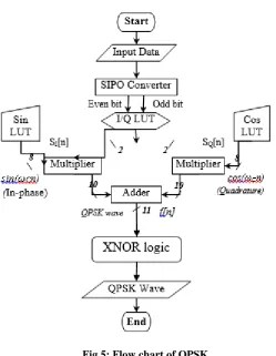
Fig 5: Flow chart of QPSK
From the above flow chart, we can observe that the input data directly given to the SIPO converter. It divides
the input data as even and odd. These even and odd are multiplied in separate multipliers with sinusoidal and
component. The outputs of both the multipliers are adder in adder block. It gives the output known as QAM.
This signal is forwarded through a XNOR logic gate to get QPSK signal i.e., output.
Simulation results and conclusion have shown in below discussions.
IV. SIMULATION RESULTS
In this paper we are designing the QPSK using the Verilog HDL and synthesised in MODEL SIM6.2.
V. CONCLUSION
The design of QPSK has designed and verified. It can able two transfer two bits per symbol using four phases
leads to minimize the chip area and decreases the power consumption. Our structure minimizes the number of
blocks to perform this technique. The obtained simulation results are verified successfully.
REFERENCES
[1] FPGA Implementation of BASK-BFSK- BPSK Digital Modulators C. Erdoğan, I. Myderrizi, and S.
Minaei ECE Department, Dogus University Zeamet Sokak 21, Acıbadem – Kadıköy, 34722 Istanbul,
Turkey.
[2] Y. H. Chye, M. F. Ain, and N. M. Zawawi, “Design of BPSK Transmitter Using FPGA with DAC,”
Proceedings of the 2009 IEEE, 9th Malaysia International Conference on Communications, December
15-17, 2009.
[3] S. O. Popescu, G. Budura, and A. S. Gontean, “Review of PSK and QAM – Digital Modulation
Techniques on FPGA,” Proceedings of the IEEE International Conference on Computational Cybernetics
and Technical Informatics (ICCCCONTI10), May 27-29, 2010, pp. 327-332.
[4] Quadrature Amplitude Modulation: A simulation study K. Kisiel, D. Sahota, G. Swaminathan, School of
Engineering Science Simon Fraser University, Canada.
[5] A Text book of Data Communications & Networking Fourth Edition by Forouzon.
[6] Modern digital and analog communication systems by B.P. Lathi.
[7] John. G. Proakis, Digital Communications, 3rd ed.: McGraw-Hill, 1995.
[8] Leon W. Couch II, "Digital and Analog Communication Systems",6th Edition, Prentice Hall, 2001.
[9] Wenmiao Song, Qiongqiong Yao, “Design and Implement of QPSK Modem Based on FPGA”.
[10] Michal Kováč “BPSK, QPSK Modulator Simulation Model”.
[11] A. Amsavalli, K.R. Kashwan, “FPGA Implementation of Low Complexity VLSI Architecture for
DS-CDMA Communication System,”, International Journal of Computer Applications (0975 – 8887), Volume
42– No.20, March 2012.
[12] G.C.Cardarilli, R. A.Del Re.RE, L.Simone Nicol, “Otimized QPSK Modulaator for DVB-S Applications,”
ISCAS 2006 IEEE.
[13] Wenmiao Song, Jingying Zhang, Qiongqiong Yao, “Design And Implement Of BPSK Modulator And
Demodulator Based On Moder DSP Technology,” IEEE International Symposium pp 1135-1137, 2009.
[14] Park, J. H., Jr., “On binary DPSK detection,” IEEE Trans. Commun., vol. 26, no. 4, April 1978, pp. 484–
486.
[15] Simon, K. M., S. M. Hinedi, and W. C. Lindsey, Digital Communication Techniques: Signal Design and
Detection, Englewood Cliffs, New Jersey: Prentice Hall, 1995.
[16] Benedetto, S., E. Biglieri, and V. Castellani, Digital Transmission Theory, Englewood Cliffs, New Jersey:
Prentice Hall, 1987.
[17] Proakis, J., Digital Communications, 2nd ed., New York: McGraw-Hill, 1989.
[18] Feher, K., Digital Communications: Satellite/Earth Station Engineering, Englewood Cliffs, New Jersey:
Prentice Hall, 1983.
AUTHOR DETAILS
THOTA MARKANDEYULU, Pursuing M.tech (VLSI) from Nalanda institute of
Engineering and Technology (NIET), Siddharth Nagar, Kantepudi village, Satenepalli
Mandal Guntur Dist., A.P, INDIA.His field of interest in designing of analog waveforms
and also specialzed in modulation techniques.
S.SIVA SANKER REDDY, he received his master degree in Signal and system
processing. His area of interest includes digital image processing, digital signal processing
with VLSI application and VLSI system design. He is currently working as Asst. professor
(ECE) from Nalanda institute of Engineering and Technology (NIET), Siddharth Nagar,