http://www.sciencepublishinggroup.com/j/eas doi: 10.11648/j.eas.20180301.11
ISSN: 2575-2022 (Print); ISSN: 2575-1468 (Online)
Methodology Article
The New Software for Research and the Modelling of
Grown-in Microdefects in Dislocation-Free Silicon Single
Crystals
Vitalyi Igorevich Talanin
*, Igor Evgenievich Talanin, Vladislav Igorevich Lashko
Department of Computer Science & Software Development, Institute of Economics & Information Technologies, Zaporozhye, Ukraine
Email address:
[email protected] (V. I. Talanin)
*
Corresponding author
To cite this article:
Vitalyi Igorevich Talanin, Igor Evgenievich Talanin, Vladislav Igorevich Lashko. The New Software for Research and the Modelling of Grown-in Microdefects in Dislocation-Free Silicon Single Crystals. Engineering and Applied Sciences. Vol. 3, No. 1, 2018, pp. 1-5. doi: 10.11648/j.eas.20180301.11
Received: December 5, 2017; Accepted: December 18, 2017; Published: January 11, 2018
Abstract:
As a virtual experimental device for research and the modelling of grown-in microdefects formation in dislocation-free silicon single crystals the software is proposed. The software is built on the basis on diffusion model of grown-in microdefects formation and allows the use of computer to investigate the defect structure of silicon monocrystals with a diameter up to 400 mm.Keywords:
Silicon, Grown-in Microdefects, Diffusion Model, Software1. Introduction
Solid-state physics is the physics of real crystals that contain structural defects [1, 2]. The problem of obtaining materials and structures with given properties is a common problem of materials science and, in particular, materials science of semiconductors. In semiconductor silicon the types, concentration and behavior of structural defects (grown-in and structural microdefects) are very diverse and depend on the nature, conditions of production and the nature of the external influences (temperature processing, pressure, irradiation, impurities, mechanical effects, etc.). Therefore, the creation of defects with the necessary properties, both in the process of crystal growth and the process of manufacturing the device, is the main way to control the properties of solid-state devices with predictable and controlled characteristics.
A set of defects determines the properties of real crystals and structures, and the additional introduction of nonequilibrium point defects during technological impacts can significantly change the thermodynamic state of crystals and structures, as well as their most important physical properties. Control of atomic processes at interfaces, reactions
between impurities and defects in materials and structures becomes one of the main trends in modern materials science and the basis of a new direction in materials science of semiconductors the defect engineering. Technologies of defect engineering are a necessary and inseparable part of semiconductor silicon manufacturing technologies and devices based on it.
Theoretical studies of defect formation in semiconductor silicon play a crucial role in the production of breakthrough ideas for next generation technologies. It is extremely important not only to grow crystals with a previously known defective structure, but also to manage this structure during the technological processes of creating devices. From this viewpoint, the diffusion model, which fully describes the kinetics of the diffusion decay processes of supersaturated solid solutions of point defects during crystal cooling after growing, depending on the thermal growth conditions, can be a convenient tool for such control [3, 4].
microdefects is performed depending on the value of crystal growth rate, temperature gradients and cooling rate of the crystal [5, 6]. Depending on the thermal growth conditions of the crystals, grown-in microdefects of three types are formed: precipitates, dislocation loops and microvoids. Experimental and theoretical studies of ultrapure dislocation-free silicon single crystals showed that the formation of a defect structure during crystal growth proceeds in the direction: from
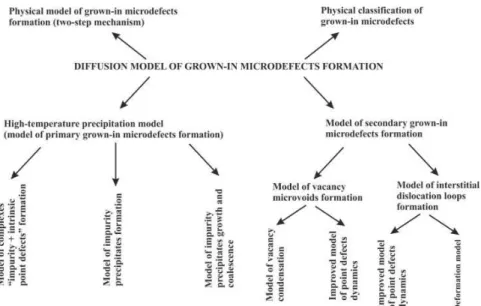
high-temperature impurity precipitation to the formation of secondary grown-in defects (microvoids or dislocation loops). The diffusion model for the formation of grown-in microdefects is based on the experimentally confirmed positions of the physical model of their formation and includes a high-temperature model of precipitation and kinetic models for the formation of microvoids and dislocation loops [7-10] (Figure 1).
Figure 1. Structural diagram of the diffusion model for the formation of grown-in microdefects.
The diffusion model is based on an experimentally and theoretically established fact that there is no recombination of IPDs at high temperatures. The model of high-temperature impurity precipitation describes the elastic interaction between IPDs and background impurities of oxygen and carbon during cooling of dislocation-free silicon single crystals after growing in the temperature range 1683K...300K. The high-temperature precipitation model includes all three stages of the classical theory of the formation of a second-phase particle: the formation of a critical nucleus, the growth and coalescence of precipitate. The process of precipitation begins near the crystallization front and is due to the disappearance of excess IPDs in the sinks, whose role is played by the impurities of oxygen and carbon. The size of the critical nucleus of the precipitate is minimal near the crystallization front and increases with decreasing temperature upon cooling of the crystal.
Under certain thermal conditions for crystal growth, depending on the growth parameter g
a
V
G in the temperature
range of cooling 1403K...1223K, either microvoids or dislocation loops are formed. Kinetic models of their formation show that the formation of microvoids has a homogeneous character, while the formation of dislocation loops occurs due to the action of the deformation mechanism. Improved models of the point defects dynamics are calculated in the absence of recombination of IPDs at high temperatures. With the practical application of the diffusion model of defect formation, two topical issues arise that are related to the purview of the model and the methodology for constructing
information complexes for the engineering of defects. First of all, it is necessary to include the problem of an adequate description of the formation and development of a defective (real) crystal structure both at the stage of their growth and at the stage of creating devices based on them. This line of research is extremely relevant for the development of the theory of solids and, moreover, has great practical importance for industrial production. Therefore, the answer to the first question implies that any theoretical model should link together the consideration of the processes of formation and development of a defective structure during the growth of a crystal and its technological treatments. The answer to the second question requires that the information system is based on the technique of analysis and calculation of grown-in microdefects adequate to the real defective structure of semiconductor silicon.
The aim of this work is to develop a new method of research of grown-in microdefects in dislocation-free silicon single crystals, based on IT-technologies.
2. The Structure of the Software System
The informational system consists of 2 sub-systems: calculation and simulation sub-systems (Figure 2). Each of these systems can be used independently or together to achieving more accurate results.
The simulation system shows the picture of the process inside the crystal, how main components are creating, growing, and merging. The formation process of defects in the crystal simulated main components which produce the biggest
influence on structure.
The user of the system should be aware that all calculations are made for ideal crystal, which doesn’t exist in real world.
Figure 2. Main screen of informational system.
The purpose of calculation sub-system is show functions and critical data of crystal growth in a graphical form. Graphs were chosen in this system (Figure 3).
The main advantage of graphs is that researcher can see all data range. That gives more broad ability to compare and analyze data series, no matter how many points each series
contains.
That is a big advantage against table view of data, where scientist can see only a several dozens of data rows. Crystals growth calculation produces many thousands of data records that makes impossible to analyze data by hand in the table view.
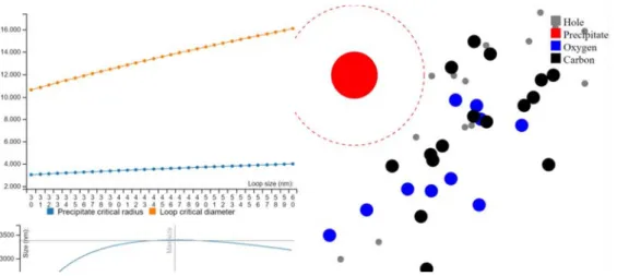
The first one calculation block calculates critical sizes of such components as precipitate and hole (Figure 4). The researcher can see linear dependency of each data series, how sizes are changing in the crystal. That gives an understanding of maximal sizes in the ideal crystal and specific parameters.
Figure 4. Thegraph of critical sizes.
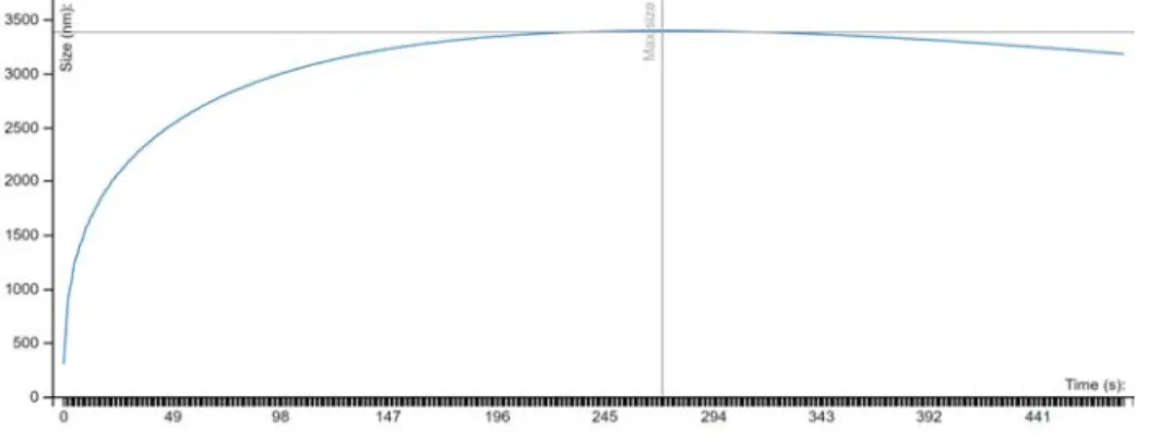
The loop’s radius graph (Figure 5) shows the evolution of loop radius at the cooling timeline, with the critical point which describes the maximal size of the loop with the description and real-time parameters. The lines from x-axis
and y-axis determinate conditions of maximal loop size, they showing specific conditions of maximal size.
This graph showing the evolution of radius, in other words, the behavior of loop during cooling time.
Figure 5. Evolution of loop radius by time.
The loop count graph (Figure 6) shows the concentrations of loops in cm3 of crystal.
Combining loop count graph with loop radius graph there can be seen dependency of loop size to loop radius which can give a more detailed picture of defects inside the crystal.
Researcher able to get a full picture of number and size of loops, because the low amount of small loops and a big amount of small loops is a different story.
It creates an average picture of the process inside the ideal crystal.
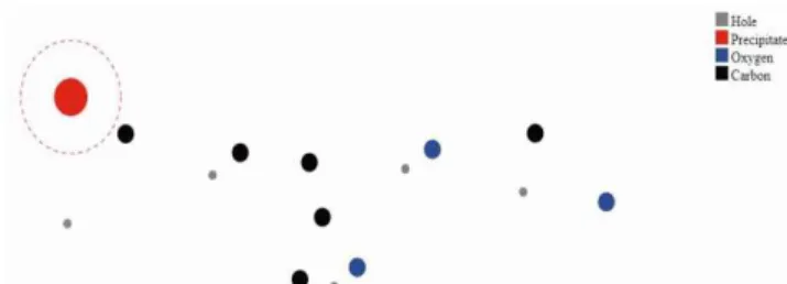
The independent simulation sub-system shows processes inside crystal during crystal growth, which allow to determinate shape and size of defects in the ideal crystal (Figure 7). The simulation shows a rough picture of what happened inside the crystal, using different parameters and components which makes the main influence on creation and evolution of the crystal’s defect structure.
Figure 7. Simulation of processes inside ideal crystal.
3. Conclusion
Theoretical study of the real structure of crystals depending on their thermal growth conditions with the help of the original virtual technique of analysis and calculation of the formation of grown-in microdefects is a new technique of experiment. This technique allows you to replace the experimental studies of the structure with adequate theoretical studies, so the software developed on the basis of the proposed method will be a new virtual experimental device.
The software complex is the first experience of using a virtual experimental device to study the real structure of dislocation-free silicon single crystals. At present, it can be used to analyze and calculate the defect structure of undoped silicon monocrystals. In this case, the software complex acts as a basis, whose improvement and refinement (for example, taking into account the interaction of point defects, dopant atoms, transition metals, nitrogen, etc.), one can expand and optimize the modeling process. Hence, the software complex for the analysis and calculation of the formation of grown-in microdefects is a universal, flexible and inexpensive tool that allows one to describe and construct real defect formation processes in dislocation-free silicon single crystals. It provides practical levers for controlling the defect structure of perfect dislocation-free silicon single crystals directly during crystal growth.
The possibility of applying a diffusion model to both crystals during their growth and to crystals after thermal effects indicates the universality of this model. The diffusion model represents a unified approach to studying the physics of defect formation processes in technologies for growing silicon crystals and technological processing of structures based on it. Hence, it is possible to analyze from a general viewpoint the formation and transformation of the defective structure of
silicon crystals from growth to the creation of various devices. Such analysis is impossible without the creation, both separate software complexes, and a single information system for analyzing the development of a defective structure. These software products can be used:
– To simulating the engineering of defects in silicon crystals during their growth.
– To simulating the engineering of defects in silicon crystals during the manufacture of devices.
– For use as a tool for studying defect formation processes in silicon.
References
[1] H. G. van Bueren, Imperfections in crystals. Amsterdam: North-Holland Publ. Company, 1960.
[2] P. Capper, "Bulk crystal growth - methods and materials." In Springer Handbook of Electronic and Photonic Materials, edited by P. Capper, and S. Kasap, 231-254. Leipzig: Springer US, 2006.
[3] V. I. Talanin, I. E. Talanin. “Diffusion model of the formation of growth microdefects: a new approach to defect formation in crystals (review).” Physics of the Solid State 58 (2016): 427-437.
[4] V. I. Talanin, I. E. Talanin, A. A. Voronin. “About formation of grown-in microdefects in dislocation-free silicon single crystals.” Can. J. Phys. 85 (2007): 1459-1471.
[5] K. Nakamura, T. Saishoji, J. Tomioka, “Grown-in defects in silicon crystals”, J. Cryst. Growth. Vol. 237-239, No. 10, 2002, pp. 1678-1684.
[6] M. Tilli, A. Haapalinna. “Properties of silicon.” In: Handbook of silicon based MEMS materials and technologies, edited by V. Lindroos, M. Tilli, A. Lehto, and T. Motooka, 3-17. Oxford: Elsevier Publ., Inc., 2010.
[7] V. I. Talanin, I. E. Talanin, “Mechanism of formation and physical classification of the grown-in microdefects in semiconductor silicon”, Defect & Diffusion Forum, Vol. 230-232, No. 1, 2004, pp. 177-198.
[8] V. I. Talanin, I. E. Talanin, “Formation of grown-in microdefects in dislocation-free silicon monocrystals”, In: Ed. T. B. Elliot, New research on semiconductors, Nova Science Publishers, Inc., New York, 2006, pp. 31-67.
[9] V. I. Talanin, I. E. Talanin, “On the recombination of intrinsic point defects in dislocation-free silicon single crystals”, Phys. Solid State, Vol. 49, No. 3, 2007, pp. 467-470.