MG2639 Module Hardware Design
User Manual
Copyright Statement
Copyright © 2010 by ZTE Corporation All rights reserved.
No part of this publication may be excerpted, reproduced, translated or utilized in any form or by any means, electronic or mechanical, including photocopying and microfilm, without the prior written permission of ZTE Corporation.
is the registered trademark of ZTE Corporation. All other trademarks appeared in this manual are owned by the relevant companies.
ZTE Corporation reserves the right to make modifications on print errors or update specifications in this manual without prior notice.
第II页 ©ZTE CORPORATION All rights reserved
This document is not allowed to transmit without ZTE
Corporation’s permission.
Descriptions of version update
Product version Document version Document No. Descriptions of document update
MG2639 V1.0 Release for the first
time
Author
Document
version Date Written by Checked by Approved by
With strong technical force, ZTE Corporation can provide CDMA/GPRS/WCDMA module customers with the following all-around technical support:
1. Provide complete technical documentation;
2. Provide the development board used for R&D, test, production, after-sales, etc.; 3. Provide evaluations and technical diagnosis for principle diagram, PCB, test scenarios; 4. Provide test environment;
ZTE Corporation provides customers with onsite supports, and also you could get supports through telephone, website, instant communication, E-mail, etc.
第IV页 ©ZTE CORPORATION All rights reserved
This document is not allowed to transmit without ZTE
Corporation’s permission.
Preface
Summary
This document introduces MG2639 module’s product principle diagram, PINs, hardware interface and module’s mechanical design, which can instruct the users how to quickly and conveniently design different kinds of wireless terminals based on this type of module.
Target Readers
This document mainly applies to the following engineers:
l System designing engineers
l Mechanical engineers
l Hardware engineers
l Software engineers
Contents
1 GENERAL DESCRIPTION OF MODULE ... 1
1.1 INTRODUCTION OF MODULE’S FUNCTIONS ... 1
1.2 MODULE’S PRINCIPLE DIAGRAM ... 2
1.3 ABBREVIATIONS ... 3
2 DESCRIPTIONS OF MODULE’S EXTERNAL INTERFACES ... 5
2.1 DEFINITIONS OF MODULE’S INTERFACES ... 5
2.2 ANTENNA INTERFACE ... 6
3 MODULE’S ELECTRICAL CHARACTERISTICS ... 8
3.1 DESCRIPTIONS OF LEVELS OF INTERFACE SIGNALS ... 8
3.1.1 RESET ... 8
3.1.2 SIM CARD INTERFACE ... 8
3.1.3 AUDIO INTERFACE ... 9
3.1.4 NETWORK SIGNAL INDICATION ... 9
3.2 MODULE POWER CONSUMPTION ... 10
3.3 RELIABILITY CHARACTERISTICS ... 10
4 INTERFACE CIRCUIT DESIGN ... 11
4.1 RESET AND POWER DESIGN ... 11
4.2 UART INTERFACE ... 12
4.3 SIM CARD INTERFACE... 13
4.4 AUDIO INTERFACE ... 14
5 MECHANICAL DIMENSIONS ... 15
5.1 APPEARANCE DIAGRAM ... 15
5.2 MODULE ASSEMBLY DIAGRAM... 15
第VI页 ©ZTE CORPORATION All rights reserved
This document is not allowed to transmit without ZTE
Corporation’s permission.
Figures
Figure 1-1 Module’s principle diagram ... 2
Figure 2-1 Antenna interface diagram ... 6
Figure 5-1 MG2639 module’s appearance ... 15
Figure 5-2 Module’s assembly diagram ... 15
Figure 5-3 Relevant PCB dimensions ... 16
Tables
Table 1-1 Module’s functions ... 1Table 1-1 28Pin stamp-hole definition ... 5
1
General description of module
This chapter mainly provides a general description of the module, including basic functions and logic block diagram.
1.1 Introduction of module’s functions
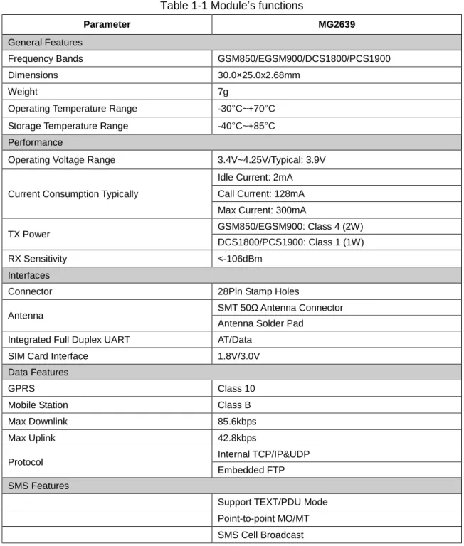
Table 1-1 Module’s functionsParameter MG2639
General Features
Frequency Bands GSM850/EGSM900/DCS1800/PCS1900 Dimensions 30.0×25.0x2.68mm
Weight 7g
Operating Temperature Range -30°C~+70°C Storage Temperature Range -40°C~+85°C Performance
Operating Voltage Range 3.4V~4.25V/Typical: 3.9V
Current Consumption Typically
Idle Current: 2mA Call Current: 128mA Max Current: 300mA
TX Power GSM850/EGSM900: Class 4 (2W) DCS1800/PCS1900: Class 1 (1W) RX Sensitivity <-106dBm
Interfaces
Connector 28Pin Stamp Holes
Antenna SMT 50Ω Antenna Connector Antenna Solder Pad
Integrated Full Duplex UART AT/Data SIM Card Interface 1.8V/3.0V Data Features
GPRS Class 10
Mobile Station Class B Max Downlink 85.6kbps Max Uplink 42.8kbps
Protocol Internal TCP/IP&UDP Embedded FTP SMS Features
Support TEXT/PDU Mode Point-to-point MO/MT SMS Cell Broadcast
第2页 ©ZTE CORPORATION All rights reserved
This document is not allowed to transmit without ZTE
Corporation’s permission.
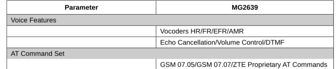
Parameter MG2639
Voice Features
Vocoders HR/FR/EFR/AMR
Echo Cancellation/Volume Control/DTMF AT Command Set
GSM 07.05/GSM 07.07/ZTE Proprietary AT Commands
1.2 Module’s principle diagram
The block diagram is used to describe the module’s major logic functions: Figure 1-1 Module’s principle diagram
1.3 Abbreviations
A
ADC Analog-Digital Converter
AFC Automatic Frequency Control
AGC Automatic Gain Control
ARFCN Absolute Radio Frequency Channel Number
ARP Antenna Reference Point
ASIC Application Specific Integrated Circuit
B
BER Bit Error Rate
BTS Base Transceiver Station
C
CDMA Code Division Multiple Access
CDG CDMA Development Group
CS Coding Scheme
CSD Circuit Switched Data
CPU Central Processing Unit
D
DAI Digital Audio interface
DAC Digital-to-Analog Converter
DCE Data Communication Equipment
DSP Digital Signal Processor
DTE Data Terminal Equipment
DTMF Dual Tone Multi-Frequency
DTR Data Terminal Ready
E
EDGE Enhanced Data Rate for GSM Evolution
EFR Enhanced Full Rate
EGSM Enhanced GSM
EMC Electromagnetic Compatibility
EMI Electro Magnetic Interference
ESD Electronic Static Discharge
ETS European Telecommunication Standard
F
FDMA Frequency Division Multiple Access
FR Full Rate
G
GPRS General Packet Radio Service
GSM Global Standard for Mobile Communications
H
HR Half Rate
I
IC Integrated Circuit
IMEI International Mobile Equipment Identity
ISO International Standards Organization
ITU International Telecommunications Union
L
LCD Liquid Crystal Display
LED Light Emitting Diode
M
第4页 ©ZTE CORPORATION All rights reserved
This document is not allowed to transmit without ZTE
Corporation’s permission.
MMI Man Machine Interface
MS Mobile Station
MTBF Mean Time Before Failure
P
PCB Printed Circuit Board
PCL Power Control Level
PCS Personal Communication System
PDU Protocol Data Unit
PLL Phase Locked Loop
PPP Point-to-point protocol
R
RAM Random Access Memory
RF Radio Frequency
ROM Read-only Memory
RMS Root Mean Square
RTC Real Time Clock
S
SIM Subscriber Identification Module
SMS Short Message Service
SMT Surface Mount Technology
SRAM Static Random Access Memory
T
TA Terminal adapter
TDMA Time Division Multiple Access
TE Terminal Equipment also referred it as DTE
U
UART Universal asynchronous receiver-transmitter
UIM User Identifier Management
USB Universal Serial Bus
USIM Universal Subscriber Identity Module
V
VSWR Voltage Standing Wave Ratio
Z
2
Descriptions of module
’
s external interfaces
This chapter mainly describes the module’s external interfaces, such as B2B connector, MINI PCI-E, stamp-hole connector, etc.
2.1 Definitions of module’s interfaces
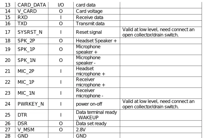
Table 1-1 28Pin stamp-hole definitionNo. Definition I/O Description Remarks
1 GND GND
2 RF_ANT I/O RF antenna
3 GND GND
4 RING O Ring signal
indication
Level varies upon an incoming call or receipt of text message.
5 GND GND
6 VBAT I Work voltage
7 RSSI_LED O Network signal
indication
Internal pull-down, LED on at high level, need add triode driver externally.
-power-on status: LED off; -network searching status: LED blinks at 3Hz
-Idle status: LED blinks at 1Hz -Traffic status (call, data): LED blinks at 5Hz.
8 RTS I Request to send
9 CTS O Clear to send
10 DCD O Carrier detection
11 CARD_RST O card reset
第6页 ©ZTE CORPORATION All rights reserved
This document is not allowed to transmit without ZTE
Corporation’s permission.
13 CARD_DATA I/O card data
14 V_CARD O Card voltage
15 RXD I Receive data
16 TXD O Transmit data
17 SYSRST_N I Reset signal Valid at low level, need connect an open collector/drain switch.
18 SPK_2P O Headset Speaker + 19 SPK_1P O Microphone speaker + 20 SPK_1N O Microphone speaker - 21 MIC_2P I Headset microphone + 22 MIC_1P I Receiver microphone + 23 MIC_1N I Receiver microphone -
24 PWRKEY_N I power on-off Valid at low level, need connect an open collector/drain switch.
25 DTR I Data terminal ready
_WAKEUP
26 DSR O Data set ready
27 V_MSM O 2.8V
28 GND GND
2.2 Antenna interface
MG2639 module provides two kinds of antenna interface:
l PCB welding pad
l Antenna test socket
PCB welding pad adopts 50Ω RF shield cable to connect the module and the antenna, in order to reduce the cost. However, using this method can’t completely shield the electromagnets, which might have slight influence on RF signal quality. Please note that there should not be strong radiation near the welding pad. Meantime, during the welding, make sure the core of RF shield cable must connect with RF welding pad, and RF shield cable’s shield metal mask must be welded to the module’s GND. During the welding, the GND must be welding securely, otherwise the core is easily broken due to the shaking of shield cable. See figure 2-1 for RF welding pad antenna.
第8页 ©ZTE CORPORATION All rights reserved
This document is not allowed to transmit without ZTE
Corporation’s permission.
3
Module
’
s electrical characteristics
This chapter mainly introduces the module’s electrical characteristics, including the level, power consumption, reliability of module’s interfaces.
3.1 Descriptions of levels of interface signals
It describes the MAX, MIN and typical value of the level of module’s external interfaces.
3.1.1
Reset
SYSRST_N PIN is used to reset the module’s main chip, and SYSRST_N signal needs to be pulled down 500ms to reset the module. Likewise, this pin is required to pull up 2.8V (Max: 2.9V, Min: 2.7V, typical: 2.8V) through 4.7K resistor inside the module, and pull down 0.1uF capacitance to GMD filtering, and it’s required to externally connect dynatron driver.
MG2639 module provides 1CH serial interface, supports 8-wire serial BUS interface or 4-wire serial BUS interface or 2-wire serial interface. The module communicates with the external devices and inputs AT commands through UART interface.
Classification Definition I/O Description Min. voltage
Typical voltage
Max. voltage
UART RXD I Receive data 2.4V 2.8V 3.1V
/RTS I Request to send 2.4V 2.8V 3.1V TXD O Transmit data 2.4V 2.8V 3.1V /DTR I Data terminal ready_WAKEUP 2.4V 2.8V 3.1V /CTS O Clear to send 2.4V 2.8V 3.1V
RING O Ring signal
indication
2.4V 2.8V 3.1V
/DSR O Data set ready 2.4V 2.8V 3.1V
DCD O Carrier detection 2.4V 2.8V 3.1V
3.1.2
SIM Card Interface
MG2639 module baseband processor integrates SIM card interface conforming to ISO 7816-3 standard, and it’s compatible with SIM card with two voltages 1.8V/3.0V and reserves SIM card interface signal on the stamp-hole PIN.
Users should note that SIM card’s electrical interface definitions are the same as SIM card socket’s definitions.
Classification Definition I/O Description Remarks
SIM V_CARD O Card voltage 1.8V/3V; maximum
output current 20mA
CARD_RST O Card reset
GND GND
CARD_CLK O Card clock
CARD_DATA I/O Card data
3.1.3
Audio Interface
MG2639 module supports 2CH audio signal inputs/outputs. It features in handheld microphone, handheld receiver or hands-free speaker and earpiece microphone/receiver function. These two MIC inputs are coupled in AC domain and the offset voltage is added inside, and they should directly connect with the receiver. The two receiver interfaces SPK_1 and SPK_2 are both differential interfaces with 32Ωresistance; SPK_2 is single-ended interface with 32Ω resistance. See the audio interface signals in the table below:
Classification Definition I/O Description Remarks
AUDIO MIC_1N I Receiver’s Microphone- The first differential receiver used for the default audio input/output and the second receiver used for headset audio input/output. MIC_1P I Receiver’s Microphone+
MIC_2P I Headset microphone +
SPK_1N O Receiver’s speaker- SPK_1P O Receiver’s speaker+
SPK_2P O Headset speaker +
3.1.4
Network Signal Indication
RSSI_LED Internal pull-down, LED turns on at high level, and need add triode driver externally. -Power-on status: LED off;
-Network searching status: LED blinks at 3Hz -Idle status: LED blinks at 1Hz
第10页 ©ZTE CORPORATION All rights reserved
This document is not allowed to transmit without ZTE
Corporation’s permission.
SIG_LED PIN output status is defined according to the software protocol, and users could judge the module’s work status according to SIG_LED status. SIG_LED PIN is common I/O port, which can’t directly drive LED, and it needs to work with dynatron.
3.2 Module Power Consumption
It describes the module’s power consumption under each status:
No. Test items Typical value(mA)
1 Power-off leakage current (Normal power-off)
50uA
2 Average standby current (no operation after power-on)
2mA
3 Average standby current (after talk)
2mA
4 Talk current 128mA
3.3 Reliability Characteristics
It describes the temperature, including working temperature and storage temperature. Working temperature: -30°C~+70°C
4
Interface circuit design
It provides the reference design circuit of the interface and precautions according to the module’s functions.
4.1 Reset and power design
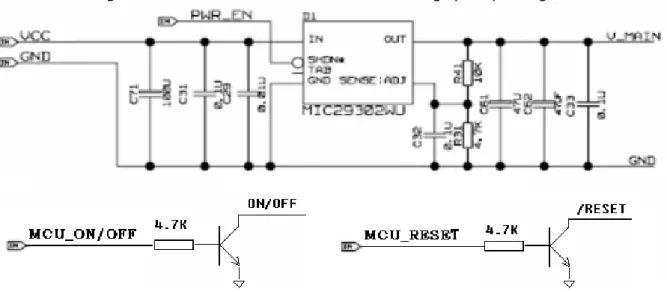
See the reference design principle of power and reset circuit in figure 4-1:
Figure 4-1 Power and reset circuit reference design principle diagram
l Power design
MG2639 module is powered by VBAT. See the voltage characteristics in table 4-1. Table 4-1 Voltage characteristics
Classification MIN Typical MAX
Input voltage 3.4V 3.9V 4.25V
Input current 2mA(average) -- 300mA(depends on the network signal)
D1 is an enabled LDO with 6V~9V input voltage. Through adjusting R31and R41, it could make V_MAIN at 3.9V to power the module, and it’s required to place at least one 1000uF tantalum capacitor at V-Main input pin. The module is very strict with the requirements on power and GND, therefore it’s requested that filtering must be performed to power and GND, and the power ripple must be controlled under 50Mv. Do not use LDO to power any other part in the system because it might affect the RF performance. Finally, select the power cables with at least 80mil traces during the layout and keep the integrality of ground line.
If MG2639 module uses other LDO, make sure the output current is larger than 2A.
l Power on
The module is under power-off status after it’s normally powered on. To turn on the module, provide a 2s-5s low level pulse to PWRKEY_N pin when the module is OFF. If one 1K resistance is connected with PWRKEY_N, the module can be turned on after power supply.
Note: ON/OFF and /Reset need to connect an open collector/drain gate. It’s not required to operate /RESET signal upon power-on.
第12页 ©ZTE CORPORATION All rights reserved
This document is not allowed to transmit without ZTE
Corporation’s permission.
l Power off
To turn off the module, use AT command “AT+ZPWROFF” or provide a 2s~5s low level pulse to PWRKEY_N PIN.
l Reset
Use the above method to firstly “power-off” and then “power-on” to hard reset the module. If the external reset function has to be used, low level pulse lasting at least 500ms should be provided to /RESET Pin within 2 seconds after the module is turned on. Before that, the external I/O signal must be kept at low level. See the reset circuit design in figure 4-1.
If SYSRST_N Pin is not used, suspend the pin.
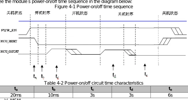
See the module’s power-on/off time sequence in the diagram below: Figure 4-1 Power-on/off time sequence
Table 4-2 Power-on/off circuit time characteristics
ta tb tc td te
20ms 10ms 3s 3s 6s
l V_MSM
There is a voltage output pin with current adjuster, which can be used to supply external power to the board. The voltage of this pin and the voltage of baseband processor/memory come from the same voltage adjuster. The voltage output is available only when the module is on. The normal output voltage is 2.85V, and the user should absorb the current from this pin as little as possible (less than 10mA). Generally, it is recommended to use this pin to match the level.
When the module is off, the output voltage for this pin remains unchanged, but the impedance is rather high. Therefore, it’s not recommended to use this pin for other purposes.
l Other advice
In order to make sure the data is saved safely, please don’t cut off the power when the module is on. It’s strongly recommended to add battery or soft switch like the power key on the module.
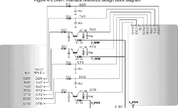
4.2 UART interface
Note: when using the module for overall design, the users should export UART for module’s software upgrade.
MG2639 module provides an integrated full duplex UART interface and an accessorial full duplex UART interface, whose maximal data rate is 115200bps. External interface is 2.8VCMOS level signal, their logic functions conform to RS-232 interface standard. These two UART could be used as serial port data interfaces, usually UART1 is used for AT commands, data transmission and updating software of module.
The module’s output IO level is 2.8V,it needs to transfer the level when connecting with standard 3.3V or 5V logic circuit(such as MCU or RS232 drive chip MAX3238 etc), Figure 4-3 shows the COM port level transfer circuit. The converted signal should connect with MCU or RS232 drive chip
directly. Common low power switch triode should be applied as the crystal triode shown in Figure 4-3. Please note that the module won’t enter sleep mode as RXD is at high level.
Figure 4-3 UART interface reference design block diagram
Remarks: the module doesn’t support USB.
4.3 SIM card interface
MG2639 module supports 1.8V or 3V SIM card, and there are 4 pins at the terminal of the card. V_CARD is used to supply SIM card. It’s strongly recommended to add ESD to protect SIM card in hostile environments.
第14页 ©ZTE CORPORATION All rights reserved
This document is not allowed to transmit without ZTE
Corporation’s permission.
NOTE: The SIM card PCB wiring should be laid closely around the module as much as possible to
prevent the interference sources from affecting the SIM card’s reading/writing. Besides, Since the
SIM card needs to be designed to meet the requirements of ESD performance and avoid the
damage of the SIM card caused by ESD, it’s recommended to add TVS components on 4-CH SIM
card signals, meanwhile, the signal wires need go through TVS component before entering the
module’s baseband processor during the layout.
4.4 Audio interface
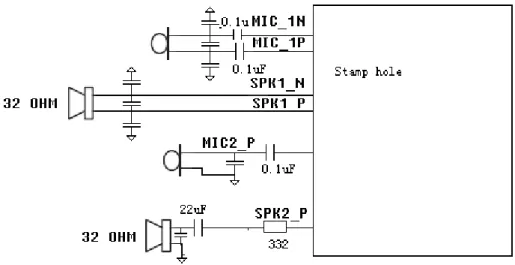
MG2639 module provides audio input and output interfaces through its PINs. There are 2 Speaker interfaces and 2 Microphone interfaces. Only one pair I/O works at the same time. See the audio interface circuit in figure 4-5.
Figure 4-5 Audio interface circuit reference design principle diagram
l Microphone
The system connector provides two microphone interfaces MIC_1 and MIC_2, MIC_1 is differential interface; while MIC_2 is single ended interface. These two inputs are coupled in AC domain and 2.0V offset voltage are added inside, therefore they should directly connect to the microphone.
l Speaker
The system connector provides two speakers, SPK_1 & SPK_2. SPK_1 is differential interface, while SPK_2 is single-ended interface. They both have 32 ohm impedance.
GSM/GPRS module audio interface is designed as below:
l Design of the audio interface on the receiver
Select the microphone with the sensitivity lower than -51.5dB since the output impedance for SPK_1 is 32 ohm and the max. gain in MIC_1 reaches 51.5dB. The level of MIC_1P PIN is about 2.2V.
Note: if other kind of audio input method is adopted, the input signal should be within 0.5V. If the
signal voltage is lower than 0.5V, then the pre-amplifier should be added. If the signal voltage is higher than 0.5V, then network attenuation should be added.
l Design of the audio interface on the headset
Select the microphone with the sensitivity lower than -51.5dB since the output impedance for SPK_2 is 32 ohm and the max. gain in MIC_2 reaches 51.5dB. The level of MIC_2P PIN is about 2.2V. The design is just the same as that on the receiver
5
Mechanical dimensions
It introduces the module’s mechanical dimensions.
5.1 Appearance Diagram
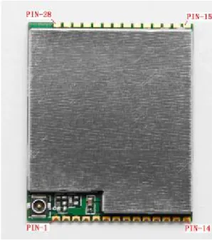
Figure 5-1 MG2639 module’s appearance
l Dimensions(L×W×H):30.0×25.0×2.68mm
l Weight:7g
5.2 Module Assembly Diagram
See the module assembly diagram in figure 5.2.第16页 ©ZTE CORPORATION All rights reserved
This document is not allowed to transmit without ZTE
Corporation’s permission.
5.3 PCB Dimensions
See the module’s PCB dimensions in figure 5-3.
Figure 5-3 Relevant PCB dimensions
Precautions while designing PCB:
1)Copper-clad and wiring are forbidden at the area below the RF test points.