Research Article
a
April
2018
Special Issue: National Conference on Emerging Trends in Engineering 2018
Conference Held at Sri Venkatesa Perumal College of Engineering & Technology, Puttur, A.P., India
Computer Science and Software Engineering
ISSN: 2277-128X (Volume-8, Issue-4)
Partial-Resonant Buck–Boost and Flyback DC–DC
Converters
Neyyikuppam.Chiranjeevi1, G Krishna Deekshit2
1
PG Student, 2 Assistant Professor 1, 2
Department of EEE, Sri Venkatesa Perumal College of Engineering &Technology, Andhra Pradesh, India
Abstract—This paper introduces innovative nonisolated and iso-lated soft-switched dc–dc topologies with the step-up/down ability. The nonisolated topology is constructed by adding a small ac ca-pacitor in parallel with the main inductor of the conventional buck– boost converter and replacing its semiconductor devices with the reverse-blocking switches. By using a novel control scheme, true zero-voltage switching is realized at both turn-on and turn-off of the power switches irrespective of the input voltage, output voltage, or load value. The isolated form of the converter is created by substi-tuting the main inductor with an air-gapped high-frequency trans-former, similar to the flyback converter. In this case, two smaller ac capacitors are placed on both sides of the transformer to realize soft switching as well as passive clamping; no extra clamping circuit is required. The basic operation of the proposed partial-resonant converters includes four modes and is described in detail. The com-prehensive analysis of the topologies is carried out as well. Various experimental results in different operating conditions are provided to verify the performance of the proposed power converters.
Index Terms—Air-gapped transformer, dc–dc converter, reso-nant power conversion, soft switching.
I. INTRODUCTION
ULSE-WIDTH modulated (PWM) dc–dc power converters Pare well developed and are widely used. These converters are simple and relatively low cost. However, PWM topologies have the disadvantages of considerable switching losses, high switching stresses, and significant electromagnetic interference due to the hard-switching operation . Soft-switching topolo-gies incorporating zero-voltage and zero-current switching have been introduced to increase the conversion efficiency, switch-ing frequency, and power density of converters. Several soft-switching dc–dc topologies have been proposed in the lit-erature; they can be mainly categorized as quasi-resonant, mul-tiresonant, resonant-transition, active-clamp, phase-controlled, and resonant-load converters. Quasi-resonant convert-ers are obtained by replacing the power switch in conventional PWM converters with a switch network containing resonant el-ements. Although the output voltage in these converters can be regulated by varying the switching frequency, the switch could suffer from excessive voltage or current stresses. Multires-onant converters are the extension of quasi-resonant converters providing soft switching for all the semiconductor devices in the circuit. Resonant-transition dc–dc converters shape the switching waveforms of the conventional PWM converters without significantly increasing the voltage and current stresses of the power devices with the expense of adding an auxiliary resonant circuit .This auxiliary circuit is composed of a switch and resonant components. Active-clamp topolo-gies employ a large capacitor and auxiliary switch to make a resonant circuit with the transformer leakage inductance in iso-lated converters, which leads to zero-voltage switching (ZVS) in addition to nondissipative voltage clamping. In a phase-controlled topology, a full-bridge network is loaded by an effective inductive load to achieve ZVS for the primary-side semiconductor devices . In this way, the switch-ing frequency is fixed and the output voltage is controlled via phase control. In resonant-load dc–dc converters, a square wave-form is applied to a resonant tank network connected to a load through a rectifier . By moving the switching fre-quency closer to or further from the resonant frequency of the tank network, the load voltage can be controlled.
According to the formation of the resonant network, resonant-load convert-ers can also be subdivided as series resonant, paral-lel resonant, series-parallel LCC resonant, and LLC topologies. Care should be taken in the consideration of various soft-switching dc–dc converters; sev-eral introduced resonant converters have noticeable drawbacks besides their soft-switching privileges. The drawbacks include poor performance over a wide range of input voltages and load resistances, poor efficiency at the light load due to current cir-culation in the tank elements, increased conduction losses, and high device voltage stress.
ISSN(E): 2277-128X, ISBN: 978-93-87396-07-4, pp. 58-65
II. PROPOSED RESONANT DC–DC CONVERTERS
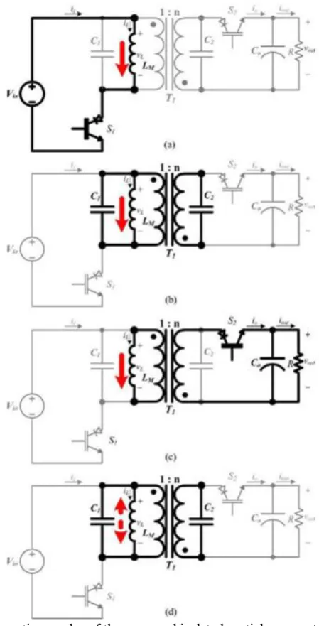
The basic partial-resonant buck–boost dc–dc converter is proposed in Fig. 1(a). Similar to the conventional buck–boost
Fig. 1. Proposed partial-resonant dc–dc converters. (a) Nonisolated buck– boost topology, and (b) isolated flyback topology.
converter, inductor L is responsible for transferring power from the input to the output. This inductor is charged from the input and then discharged to the output cycle-by-cycle. Small ac ca-pacitor C is placed in parallel with this inductor. The main role of capacitor C is to produce partial resonances with the induc-tor to realize ZVS for the power devices, as will be shown later. As the figure depicts, the converter needs two (RB switches. An RB-switch can be realized by a conventional reverse-conducting switch (IGBT or MOSFET) in series with a diode. However, the newly available individual RB-switches can be employed with the advantage of lower total on-state voltage [28].
Fig. 1(b) shows the isolated topology. In this converter, the magnetizing inductance of the high-frequency transformer is used for transferring power. In order to reach an appropriate inductance value, the transformer may need to have an air gap.
Two smaller capacitors, C1 and C2 , provide partial resonance. These capacitors are placed on both sides of the
transformer to also provide paths for the currents of the primary and sec-ondary leakage inductances and subsequently, avoid voltage spikes when the input and output switches are turned OFF [27]. As a result, no extra snubber circuit is required.
III. PRINCIPLE OF OPERATION
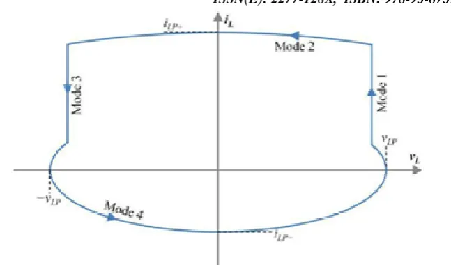
The operation of the proposed soft-switched dc–dc converter in both nonisolated and isolated configurations is composed of four modes in each switching cycle.
ISSN(E): 2277-128X, ISBN: 978-93-87396-07-4, pp. 58-65 The converter’s main inductance charges through the input in mode 1 and discharges to the output in mode 3. Modes 2 and 4 are for partial resonance of the main inductance with its parallel capacitance to achieve ZVS at both turn-on and turn-off of the power switches. A typical switching cycle of the isolated partial-resonant topology is shown in Fig. 2, and its corresponding operating modes are shown in Fig. 3. The state-plane diagram is also depicted in
Fig. 4. The detailed operating modes of the isolated converter are explained in detail as follows by ignoring the transformer’s leakage inductances and winding resistances. Their effects will be shown later.
A. Mode 1 [Inductance Charges From the Input, Fig. 3(a)]
Switch S1 is turned ON to connect the input dc voltage across the magnetizing inductance of the transformer, LM . As a
result, LM charges in the positive direction. This mode is allowed to rununtil the average of the input current meets the input reference current, Ii∗. Subsequently, switch S1 is turned OFF.
Note that due to the existence of capacitors C1 and C2 , the magnetizing inductance voltage, vL (t), decreases slowly when
switch S1 is turned OFF. As a result, the voltage of switch S1 goes up slowly in its off transition. Therefore, the
turn-off of switch S1 occurs at almost zero voltage. Switch S2 has a similar ZVS in its turn off. As the ZVS behavior at the
turn-off of the power switches is caused by the existence of C1 and C2 , it happens at any input voltage, output voltage, or
load value.
Fig. 3. Operating modes of the proposed isolated partial-resonant converter. (a) Mode 1, (b) mode 2, (c) mode 3, (d) mode 4.
B. Mode 2 [Partial Resonance, Fig. 3(b)]
LM starts to partially resonate with its total parallel capaci- tance, Ct = C1 + n2 C2 (n is the transformer’s turns ratio), and therefore, vL (t) starts to drop. This partial resonance is per- mitted to run until vL (t) becomes equal to the output reflected voltage (−Vo u t/n), which then allows the converter to go to mode 3 with soft transition. During this mode,
ISSN(E): 2277-128X, ISBN: 978-93-87396-07-4, pp. 58-65
Fig. 4. State-plane diagram of the proposed converter.
where IE1 is the magnetizing inductance current at the end of mode 1, and Vin is the input dc voltage.
C. Mode 3 [Inductance Discharges to Output, Fig. 3(c)]
The load-side switch, S2 , is turned ON to discharge the mag-netizing inductance energy to the output. This mode
continues until iL (t) reaches a small value of IE3 , which will be defined later. After that, this mode ends and switch S2
turns OFF. In order to leave a certain amount of current in LM at the end of mode 3 in the digital control implementation,
iL(t) is constantly measured.
Once iL(t) reaches the desired value, switch S2 is turned OFF and the converter goes to mode 4.
The magnetizing inductance voltage is equal to the output reflected voltage at the beginning of mode 3 when switch S2 is
turned ON. As a result, the turn-on transition of switch S2 occurs at zero voltage. The zero-voltage turn-on also happens
for switch S1 similarly. This ZVS at the turn-on of the power switches does not depend on the load level and voltage
values.
D. Mode 4 [Partial Resonance, Fig. 3(d)]
LM and Ct resonate together again. This considerable partial resonance is maintained until vL (t) is equal to the input voltage in the down-going direction, which then permits the converter to go to mode 1 with soft transition. Therefore, vL (t) should go higher than the input voltage during this mode as shown in Fig. 2.
In the case that Vo u t/n is more than the input voltage, this process happens naturally, and IE3 can be selected as zero (the
peak value of the magnetizing inductance voltage, VL P , will be equal to Vo u t /n). However, when Vo u t /n is smaller
than the input voltage, a certain amount of current should be left in the magnetizing inductance at the end of mode 3 to force vL (t) to peak higher than the input voltage as follows:
The proposed converters’ control scheme only requires the measurement of the main inductance voltage and current as they include the information of the input and output voltages and currents. In case of the isolated topology where the mag-netizing inductance current cannot be measured directly, the transformer’s primary and secondary currents should be mea-sured and properly subtracted (by including the turns ratio) to reach the magnetizing inductance current. Note that by knowing the exact value of the main inductance in the isolated and noniso-lated topologies, the inductance current can be easily estimated, and only the inductance voltage measurement is required.
In the digital control implementation of the proposed convert-ers, the switches may be turned ON with a delay from the exact desirable instants due to the discrete sampling. This delay may create an unwanted hard-switching operation. In order to avoid this problem, the switches can be turned ON sooner while they have negative voltages. The switches do not conduct at this time because they are RB switches and their voltages are negative. Once they become forward biased, they start conducting. By us-ing this switching scheme, ZVShappens truly for both switches. Switch S1 can be turned on
when vL(t) reaches its positive peak value, and switch S2 can be turned ON as soon as the switch S1 is turned OFF. As
Fig. 2 shows, once vL(t) reaches its positive peak value, iL(t) passes zero in the positive direction. So, the zero crossing of iL(t) can be used as a sign to appropriately turn on switch S1.
ISSN(E): 2277-128X, ISBN: 978-93-87396-07-4, pp. 58-65 Therefore, the magnetizing inductance and the total par-allel capacitance were selected as 225μH and 100 nF to set the
switching frequency at about 22 kHz atthe given operating point. The switching frequency can be moved higher
provided that a faster digital controller with a smaller sample time is em-ployed. The proposed control scheme can also be implemented by using an FPGA or integrated analog design, which mainly eliminates this problem. Although the proposed partial-resonant isolated dc–dc con-verter can work with the transformer’s turns ratio of 1 in both step-up and step-down operations, the turns ratio can be selected optimally for the optimal operation.t. As the graph shows, the magnetizing inductance rms cur-rentreaches its lowest value when n is almost equal to 0.92 for the input voltage of 300 V (same as the output voltage). This oc-curs because as the turns ratio decreases from unity, the mode-3magnetizing inductance voltage, −Vo u t/n, decreases. If Vo u t/nreaches the required peak value of the magnetizing inductance voltage,
there is no need to leave any current in the magnetizinginductance at the end of mode 3 as stated before .Fig. 8 shows the switching frequency and the magnitudes of the magnetizing current peak values versus the output power for different values of the input voltage. According to the figure, the positive peak value of the magnetizing inductance current is completely dependent on the output power, and as the out-put power reduces, IL P + decreases almost linearly. Thisoccurs
because as the output power drops, the input reference cur-rent should decrease accordingly. Therefore, the time-lengths of modes 1 and 3 decrease, which results in thereduction of IE1 in (1) and consequently IL P + . In addition, thereduction in
duration of the odd-numbered modes results in the increase of the switching frequency. Note that according to (3),IL P −
does not depend on the output power, but it may dependon the input voltage (VL P should be higher than the input
voltage). The switching frequency and the magnitudes of themagnetizing current peak values at a very small amount of the output power can be given.According to Fig. 8, the change of the input dc voltage at a given output power affects the operating parameters of the pro-posed converter moderately. Although the increment of the input voltage at any given power increases the switching frequency,the change of the peak values of the magnetizing inductance current depends on the output power and input voltage values at the operating point of the converter.
V. EXPERIMENTAL RESULTS
To test the performance of the proposed topology, a pro-to type of the proposed isolated partial-resonant converter was built and tested as shown in Fig. 9. TMS320F28335 microcon-troller was employed to control the prototype converter. The sample time of the digital control was minimized to reach bet-ter control performance, which resulted in the sample time of 1.1 μs.
Fig. 9. Developed prototype of the proposed isolated topolgy.
ISSN(E): 2277-128X, ISBN: 978-93-87396-07-4, pp. 58-65 secondary-side magnetizing inductance of 225 μH and turns ratio of 0.92. Since the transformer has a considerable air gap length with a high-frequency ac current, the air gap fringing field can cause huge eddy current losses in adjacent coil con-ductors [30]. To avoid this problem, windings were not placed in the immediate vicinity of the gap and multistranded
wires were employed. The total leakage inductance and winding re- sistance of the transformer were measured as 2 μH
and 95 mΩ, respectively. The parallel capacitors C1 and C2 were chosen as 47 nF to have Cs of about 103 nF at the
primary-side of the transformer.
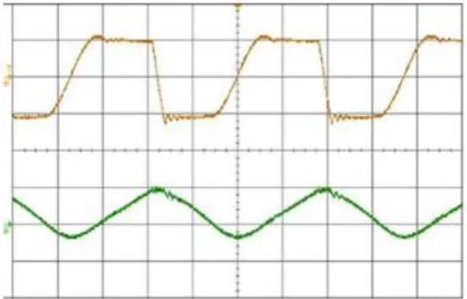
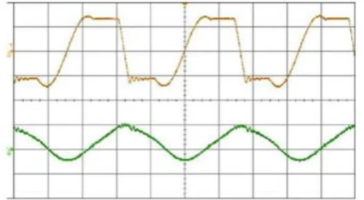
In the first test, the prototype converter was run with the in-put voltage of 300 V to supply 750 W to a 120 Ω load, which yielded the output voltage of 300 V. Fig. 10 shows the mag-netizing inductance current and the transformer primary-side voltage, which is almost equal to the magnetizing inductance voltage. As the figure shows, the transformer’s leakage induc-tances cause some ringing at the beginning of modes 1 and 3, which are damped by the parallel capacitors and dissipated in the winding resistances of the transformer. The resulting switching frequency and the positive and negative peak values of the mag-netizing inductance current were 22.4 kHz, 18.9 A, and −6.4 A, respectively, at this test condition. These values are very close to the analytical results shown in Fig. 8. The small differences are mainly due to the nonlinearity and power loss of the com-ponents. The measured efficiency was 96.2%. Figs. 11 and 12
Fig. 11. Experimental results with 300 V input at 750 W. Top: voltage of switch S1 (400 V/div), and bottom: current of switch S1 (20 A/div) versus time (5 μS/div).
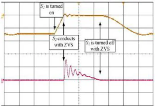
Fig. 12. Experimental results with 300 V input at 750 W. Top: voltage of switch S2 (400 V/div), and bottom: current of switch S2 (20 A/div) versus time (5 μS/div).
depict the voltage and current waveforms of switches S1 and S2 . As the figure shows, the true ZVS happens at both
turn-on and turn-off of the power switches as expected. The magnetizing inductance voltage and current of the prototype converter with the output power of 375 W (50% nominal load) and 75 W (10% nominal load) are displayed in Figs. 13 and 14. As the figures show, reducing the output power mainly decreases the duration of the odd-numbered modes where power is transferred. The switching frequency for the output power of 375 and 75 W was measured as 25 and 30.1 kHz, respectively, which is in agreement with the analysis results shown in Fig. 8. The soft transitions between the modes clearly verify the soft-switching operation of the converter in these cases.
ISSN(E): 2277-128X, ISBN: 978-93-87396-07-4, pp. 58-65
Fig. 13. Experimental results with 300 V input at 375 W. Top: magnetizing inductance voltage (300 V/div), and bottom: magnetizing inductance current (20 A/div) versus time (12 μS/div).
Fig. 14. Experimental results with 300 V input at 75 W. Top: magnetizing inductance voltage (300 V/div), and bottom: magnetizing inductance current (20 A/div) versus time (12 μS/div).
Fig. 15. Experimental results with 200 V input at 750 W. Top: magnetizing inductance voltage (300 V/div), and bottom: magnetizing inductance current (20 A/div) versus time (12 μS/div).
ISSN(E): 2277-128X, ISBN: 978-93-87396-07-4, pp. 58-65
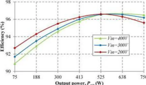
Fig. 17. Efficiency of the prototype converter versus output power for different values of the input voltage.
that the magnetizing inductance current at the end of mode 3 is zero with the input voltage of 200 and 300 V (see Figs. 10 and 15) while it is nonzero with the 400 V input (see Fig. 16), ac-cording to (2). As a result, VL P and |IL P−| are higher
in Fig.
16.The measured efficiency of the designed partial-resonant fly-back converter versus the output power for different values of the input voltage is shown in Fig. 17. The efficiency of the conventional flyback converter was measured 1.9% lower than the proposed converter at nominal operating condition. This de-crease was 3.5% at light-load condition. Note that the switching frequency of the prototype converter was limited by the digital controller sampling rate. In case a faster controller is used, the switching frequency can be selected higher, and as a result, the partial-resonant converter can show more advantage in terms of efficiency.
VI. CONCLUSION
Fig. 15 and increased in Fig. 16. As a result, the mode-1 dura-tion is increased with the 200 V input and decreased with the 300 V input to draw the same amount of power from the input.
Therefore, consistent with the analytical results, the switching frequency decreased to 18.7 kHz in the step-up operating case and increased to 24.6 kHz in the step-down test condition.
A new generation of soft-switched buck–boost dc–dc convert-ers was introduced in this paper. The partial-resonant network is composed of a small inductor in parallel with a small ac ca-pacitor. The main role of the inductor is to transfer power by charging from the input and discharging to the output or vice versa. The parallel capacitor creates partial resonances to realize zero-voltage turn-on and turn-off for the converter’s switches.
The inductor can be simply replaced by an air-gapped high-frequency transformer to achieve galvanic isolation. Detailed analysis of the proposed topology was given to reveal its be-havior at various operating points. According to this analysis, the converter’s main components can be properly selected to fit the desired working conditions. Multiple experimental results were presented to demonstrate the effective performance of the proposed topology in different operating conditions.
REFERENCES
[1] M. K. Kazimierczuk and D. Czarkowski, Resonant Power Converters, 2nd ed. Hoboken, NJ, USA: Wiley, 2011.
[2] R. Erickson and D. Maksimovic, Fundamentals of Power Electronics, 2nd ed. New York, NY, USA: Kluwer,
2004.
[3] I. Aksoy, H. Bodur, and A. F. Bakan, “A new ZVT-ZCT-PWM DC–DC converter,” IEEE Trans. Power
Electron., vol. 25, no. 8, pp. 2093–2105, Aug. 2010.
[4] K. H. Liu and F. C. Lee, “Zero-voltage switching technique in DC/DC converters,” IEEE Trans. Power