A New Zcs-Pwm Full-Bridge Dc–Dc Converter With Simple Auxiliary
Circuits
Ramalingeswara Rao M1, Mr.B,D.S.Prasad2 1
PG Scholar, Pydah College of Engineering, Kakinada, AP, India. 2Assistant Professor, Pydah College of Engineering, Kakinada, AP, India.
Abstract— In this paper design & analysis of pv system based full bridge dc-dc converter with auxiliary circuits with soft-switching pulse width modulated (PWM) converter is proposed. The advantage of this converter is that it allows its main power switches to operate with zero current switching (ZCS) and with fewer conduction losses than conventional full-bridge converters. This conventional approach will gathered importance towards solar system. This solar system is also designed by using two simple active auxiliary circuits one is active, and the other is passive. The paper presents the PV based converter system and then discusses its operation, steady-state characteristics. Simulation results will be obtained from MATLAB/SIMULINK software to validate the converter’s performance of the PV system based full bridge dc-dc converter.
Index Terms—Bidirectional converters, dc–dc converters, zero-current switching (ZCS) converters, PV system
I. INTRODUCTION
For higher power applications, where IGBTs are the preferred devices as they have lower conduction losses than MOSFETs due to their fixed collector–emitter voltage drop, zero-current-switching (ZCS) techniques are preferred. This is because ZCS methods can significantly reduce the tail in the IGBT device current that appears when the device is turned off. Reducing this current tail helps an IGBT operate with fewer turn-off losses and allows it to operate at higher switching frequencies. Previously proposed soft-switching techniques for higher power dc–dc full-bridge converters have at least one of the following drawbacks: 1) They are resonant techniques in which resonant elements such as capacitors and inductors are used to shape the current through a converter switch so that it can fall to zero to allow the switch to turn off with ZCS. The resonant elements, however, are large and bulky, which makes their use impractical for many applications, and the converter is operated with variable frequency control, which makes the design of the converter more difficult and also increases the size of the converter as it must operate with low switching frequencies at lighter loads.
2) They are ZCS-PWM techniques that use active auxiliary circuit consisting of active switches and passive components to help the main converter switches turn off with ZCS. Most of these techniques use complicated auxiliary circuits to remove current from the main switches to turn off the main switches with ZCS; for example, auxiliary circuits with two auxiliary switches are proposed in [13]–[18] to achieve ZCS for the main switches. The increased cost of having two
auxiliary circuits, however, is a key drawback of these converters as it increases their cost and complexity.
3) They are passive snubber techniques. Although the use of multiple auxiliary switches is avoided with these converters, the passive circuits themselves can be quite sophisticated and the overall converter efficiency is lower than that of the aforementioned converters that use multiple auxiliary switches.
4) They are zero-voltage–zero-current-switching (ZVZCS) techniques. These techniques either use a secondary-side auxiliary switch or a secondary-side passive circuit to create a counter voltage in the converter primary that helps extinguish the current that would otherwise circulate in the full-bridge whenever the converter is in a freewheeling mode and do nothing but create conduction losses. Regardless of what method is used to extinguish the freewheeling current, ZVZCS converters allow only their lagging leg switches to operate with ZCS so that IGBTs cannot be used in their leading leg. This forces the use of MOSFETs in this leg instead of IGBTs to avoid high current losses at turn-off. As a result, not only does this increase the price of these converters as two different types of devices must be used as the main power switches in the converter, but the converter is limited to lower power applications due to the specifications of MOSFETs.
5) They require the placing of reverse blocking diodes in series with main power switches to prevent current from flowing through their body diode or require that IGBTs with reverse blocking capability be used. The use of reverse blocking devices increases the amount of conduction losses in the converter, thus reducing converter efficiency.
A new ZCS-PWM full-bridge converter is proposed in this paper. The outstanding feature of the new converter is that it allows its main power switches to operate with ZCS and with fewer conduction losses than conventional full-bridge converters. This is achieved by using two very simple active auxiliary circuits—one active with a switch that can turn on and off with ZCS and one passive that consists of a few passive components.
II. CONVERTER OPERATION
Fig. 1 Proposed ZCS converter
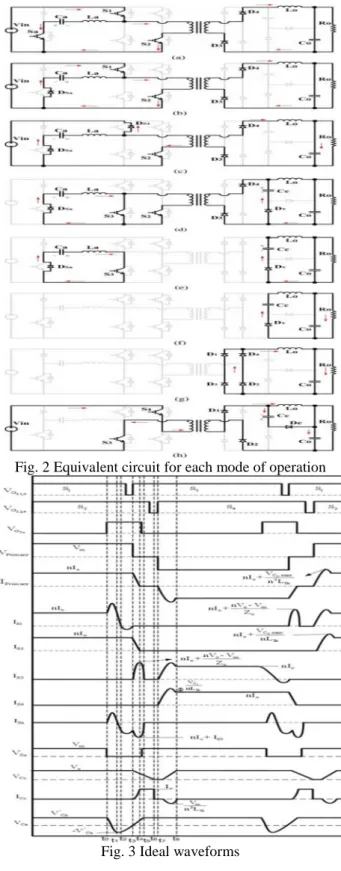
Equivalent circuit diagrams of the modes of operation that the proposed converter goes through during a half switching are shown in Fig. 2 and ideal converter waveforms are shown in Fig. 3. It should be noted that in Fig. 3, a current waveform such as IS1 shows the current flowing through a switch (positive part of the waveform) and its body diode (negative part of the waveform).
Moreover, the ISa waveform is also the waveform for ILa and ICa as ISa = ILa = ICa andV _Ca on the VCa waveform can be considered to be equal to the input voltage.
The converter’s modes of operation are as follows:
Mode 1 (t0≤ t ≤ t1) [see Fig. 2(a)]: Switches S1 and S2 are on before this mode and the input power is transferred to the output through D3 and D4. At the beginning of this mode, auxiliary switch Sa is turned on and Ca starts to discharge, resonating with La. This mode ends when the current flowing through Sa reaches zero. From the equivalent circuit of Mode1 shown in Fig. 4(a), the primary currents and voltages can be expressed as
Where n is the transformer ratio, Llk the leakage inductance,
IS1 the instantaneous current through switch S1, Iin the
instantaneous input current, ILa the current through inductor
La, ILl k the current through the leakage inductance and is
equal to the primary current Iprimary, VCa the voltage across capacitor Ca , and Vo is the output voltage.
The initial conditions for (2) and (3) are VCa (t0) =
Vin , ILa (t0) = 0, and ILl k (t0) = nIo , where n is the
transformer turns ratio n = n2 /n1 and Io is the output current. For simplicity, the primary current during this mode is approximated as the reflected primary current nIo . Solving these equations gives
Fig. 2 Equivalent circuit for each mode of operation
Fig. 3 Ideal waveforms
Where Vin is the input voltage and
Mode 2 (t1≤ t ≤ t2) [see Fig. 2(b)]: At the beginning of this mode, current in Sa starts flowing in the opposite direction from its flow in Mode 1, through the anti-parallel diode of
Sa , i.e., DSa . Sa can be turned off softly while current is
flowing in DSa. Voltage across Ca starts increasing as Ca resonates with La. Current in S1 starts decreasing in this mode and reaches zero at the end of this mode. The currents
IS1 and ICa = ILa follow the same equations as in Mode 1.
The equivalent circuit of Mode 2 is shown in Fig. 4(b). It is very similar to that of Mode 1except that the direction of
ICa = ILa current is different due to it being the negative
portion of a resonant cycle.
Mode 3 (t2≤ t≤t3 ) [see Fig. 2(c)]: At the beginning of this mode, current in S1 starts flowing in the reverse direction through the anti-parallel diode of S1 , i.e., DS1 ; therefore,
S1 can be turned off in this mode softly with ZCS. The
voltage across Ca continues to rise as Ca resonates with La. The current in the auxiliary switch flows in the negative direction, through DSa. The equivalent circuit of Mode 3 is shown in Fig. 4(c). The voltage across Ca and the current flowing through La can be expressed according to the following equations:
The initial conditions for (8)–(10) are VCa (t2) = −nIoZ1
and iLa (t2) = nIo . Solving these equations gives
Where
Mode 4 (t3≤ t ≤ t4) [see Fig. 2(d)]: At the beginning of this mode, S3 is turned on softly as the rise in switch current is constrained by the presence of La and transformer leakage inductance. During this mode, diode Dv becomes forward biased and the voltage across Cc appears across the transformer secondary. This voltage is reflected to the primary as a counter voltage that helps extinguish the primary current and thus the current through S2. Cc is discharging throughout this mode. The voltage and current in auxiliary inductor La can be found from the following equations in this mode:
The initial conditions for (15) and (16) are VCa (t3) = 0 and
iLa (t3) = nIo . Solving these equations gives
Mode 5 (t4≤ t ≤ t5) [see Fig. 2(e)]: This mode begins when current in S2 has reached zero. S2 can be turned off with ZCS sometime after the start of this mode. During this mode, current continues to flow through the body diode of
Sa and S3. Cc supplies the load current and the voltage
across it continues to drop.
Mode 6 (t5 ≤ t ≤ t6) [see Fig. 2(f)]: Current has stopped flowing through the primary of the converter at the beginning of this mode. S3 can be turned off with ZCS during this mode as there is no current flowing in the primary side. Capacitor Cc continues to discharge.
Mode 7 (t6≤t≤t7) [see Fig. 2(g)]: This mode begins when
Cc has been completely discharged. DiodesD1 − D4 start
conducting at the beginning of this mode and the load current freewheels through them afterward.
Mode 8 (t7≤ t ≤ t8) [see Fig. 2(h)]:At the beginning of this mode, S4 is turned on softly and the current through it rises gradually since the primary current cannot change suddenly due to the transformer leakage inductance. Energy is transferred to the secondary side of the converter through D1 and D2. Voltage across Cc rises through Dc resonating with the leakage inductance of the transformer. It should be noted that the proposed converter can be implemented using standard phase-shift PWM.
III. CONVERTER FEATURES AND DRAWBACKS The proposed converter has the following features:
1) The voltage across secondary circuit capacitor Cc is reflected to the converter primary when the converter is in a freewheeling mode of operation (Mode 4). This is the mechanism that extinguishes the freewheeling current, which reduces conduction losses and allows the lagging leg switches to turn off with ZCS.
2) The leading leg switches turn off with ZCS as the primary side auxiliary circuit injects current into their body diodes before they are turned off. In the case of S1, as seen in Fig. 2, this body-diode current is generated by first charging Ca after Sa is turned on, then having the current through La and
Ca reverse direction and flow through the body diode of S1
after Ca has been charged to its peak value. In the case of
S2, which is not shown in Fig. 2, Ca has negative voltage
3) Sa can be turned off with ZCS (Mode 3) as the Ca− La
resonant circuit forces current through the switch to be gradually removed then flow through its body diode. 4) All converter switches turn on with ZCS because they either have an inductor in series with them (main transformer leakage inductance for S2 and S4, La for Sa) or the current in the series is constrained by the presence of other inductances in circuit (La and the main transformer leakage inductance for S1 and S3 ).
5) Due to the gradual rise and fall of the primary current during any switching transition, the secondary diodes turn off softly. Moreover, Cc acts a clamping capacitor to suppress any voltage ringing that may appear across the secondary diodes. The converter is based on a ZVZCS converter and, thus, has the features of converters of this type.
It should be noted that neither the active auxiliary circuit nor the passive auxiliary circuit are new individually, by themselves. The active auxiliary circuit can be any one of a number of previously proposed ZCS-PWM converter active auxiliary circuits and the passive auxiliary can also be any one of a number of previously proposed passive auxiliary circuits used in previously proposed ZVZCS-PWM converters. The auxiliary circuits chosen for the proposed converter were chosen as they are among the simplest of each type.
What is new and novel about the proposed converter is that the combination of an active ZCS auxiliary circuit and a passive ZVZCS auxiliary circuit has never been
previously proposed before to the best of the authors’
knowledge. It is this combination that allows the converter to have a very simple topology that can be implemented with IGBTs for all four main power switches and with ZCS turn-on and turn-off for all four switches and the active auxiliary switch as well. These properties cannot be found in previously proposed ZVZCS full-bridge converters, which have leading leg switches that must operate with a ZVS turn-on (which is unsuitable for IGBTs) nor can they be found in previously proposed ZCS full-bridge converters, which require more sophisticated topology, blocking diodes, and/or bulky resonant components.
The proposed converter, however, has the following drawbacks:
1) Since it is a ZCS-PWM converter, it is not a suitable topology if a converter is to be implemented with MOSFETs it is standard practice to operate MOSFETs with ZVS. 2) The current in any given switch in the proposed converter will have a resonant peakso that the converter’s peak switch
current will be higher than that of a switch in a ZVS-PWM converter.
3) The light load efficiency of the converter is worse when the active auxiliary circuit is implemented than when it is not. This is because the turn-off losses of the leading leg switches to which the active auxiliary circuit is attached are fewer than the losses of the active auxiliary circuit when the converter is operating under light load conditions. The opposite becomes true at heavier loads. It should be noted that all the aforementioned drawbacks are common to ZCS-PWM converters in general.
IV. SIMULATION RESULTS
Fig 5 simulation diagram of proposed system with PV system
Fig. 6 Current and voltage waveforms in S1
Fig. 7 Current and voltage waveforms in S3
Fig. 8 Current and voltage waveforms in S2
Fig. 9 Primary voltage waveform across the transformer
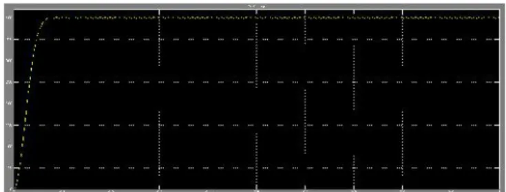
Fig 11 Proposed ZCS converter output voltage
CONCLUSION
In this paper design & analysis of pv system based full bridge dc-dc converter with auxiliary circuits with soft-switching pulse width modulated (PWM) converter is proposed. The outstanding feature of the new converter is that it allows its main power switches to operate with ZCS and with fewer conduction losses than conventional full-bridge converters. This is achieved by using a very simple active auxiliary circuit and a ZVZCS technique so that the converter has all the advantageous features of ZVZCS converters but with ZCS operation for all the converter switches so that they can all is IGBT devices, which helps reduce component cost.
The proposed converter does not have the drawbacks of previously proposed techniques for higher power dc–dc full-bridge converters with IGBTs, including resonant techniques, ZCS-PWM techniques with active auxiliary circuits, passive techniques, ZVZCS techniques, and techniques that require the use of reverse blocking diodes. Results obtained confirm the feasibility of the converter and show that the active auxiliary circuit results in a maximum efficiency improvement of 7% compared to the conventional ZVZCS converter due to the elimination of leading leg turn-off losses by the active auxiliary circuit.
REFERENCES
[1] C. Liu, B. Gu, J. Lai, M. Wang, C. Zheng, Y. Ji, and P.
Sun, “Highefficiency hybrid full-bridge–half-bridge converter with shared ZVS lagging leg and dual outputs in
series,” IEEE Trans. Power Electron., vol. 28, no. 2, pp.
849–861, Feb. 2013.
[2] K. Jin, Y. Sun, M. Xu, D. Sterk, and F.C. Lee,
“Integrated magnetic selfdriven ZVS nonisolated full-bridge
converter,” IEEE Trans. Ind. Electron., vol. 57, no. 5, pp.
1615–1623, May 2010.
[3] X. Zhang, W. Chen, X. Ruan, and K. Yao, “A novel
ZVS PWM phaseshifted full-bridge converter with controlled auxiliary circuit,” in Proc. IEEE APEC, Feb.
2009, pp. 1067–1072.
[4] I. Lee and G. Moon, “Soft-switching dc/dc converter with a full ZVS range and reduced output filter for
high-voltage applications,” IEEE Trans. Power Electronics, vol.
28, no. 1, pp. 112–122, Jan. 2013.
[5] W. Chen, X. Ruan, and J. Ge, “A novel full-bridge converter achieving ZVS over wide load range with a
passive auxiliary circuit,” inProc. IEEE ECCE, Sep. 2010,
pp. 1110–1115.
[6] D. Sterk, M. Xu, and F.C. Lee, “High frequency ZVS self-driven fullbridge using full integration of magnetics,” in Proc. IEEE APEC, 2010, pp. 1210–1216.
[7] Z. Chen, M. Chen, F. Ji, and J. Li, “Analysis and
implementation of a novel full-bridge ZVS converter with
adaptive auxiliary circuit,” in Proc. IEEE IECON, Nov.
2010, pp. 358–363.
[8] H. L. Do, “Improved ZVS Dc–dc converter with a high voltage gain and a ripple-free input current,” IEEE Trans. Circuits Syst., vol. 59, no. 4, pp. 846–853, Apr. 2012. [9] J. Sun, X. Ding, M. Nakaoka, and H. Takano,“A novel
series resonant ZCS full bridge three-level dc–ac inverter,”
in Proc. IEEE APEC, 2008, pp. 419–425.
[10] W. Huai, S. Qian, H. Chung, S. Tapuchi, and A.
Ioinovici, “Series resonant ZCS-PFM DC–DC converter with multistage rectified voltage multiplier and dual-mode PFM control scheme for medical-use high-voltage X-ray
power generator,” IEEE Trans. Electric Power Appl., vol.
147, no. 6, pp. 527–534, Aug. 2000.
[11] W. Chen, Y. Gu, and Z. Lu, “A novel three Level full
bridge resonant dc–dc converter suitable for high power
wide range input applications,” in Proc. IEEE APEC,
Feb./Mar. 2007, pp. 373–379.
[12] M.S. Agami and P. Jain, “A new full bridge three level resonant single stage AC/DC converter,” in Proc. IEEE PESC, Jun. 2007, pp. 2699–2704.
[13] W. Huai, S. Qian, H. Chung, S. Tapuchi, and A.
Ioinovici, “A ZCS currentfed full-bridgePWMconverter with self-adaptable soft-switching snubber energy,” IEEE Trans. Power Electron., vol. 24, no. 8, pp. 1977–1991, Aug. 2009.
[14] K. Fathy, T. Doi, K. Morimoto, H. Lee, and M.
Nakaoka, “A novel soft-switching PWM full-bridge DC/DC converter with DC busline series switch-parallel capacitor edge resonant snubber assisted by highfrequency
transformer leakage inductor,” inProc. IEEE IPEMC, Aug.
2006, pp. 1–5.
[15] K. Suzuoka, S. Moisseev, L. Gamage, K. Soshin, K.
Nishida, and M. Nakaoka, “Boost transformer linked full
bridge soft-commutation DC–DC power converter with secondary-side phase-shifted PWM rectifier switches,” in Proc. IEEE IECON, Nov. 2003, pp. 49–54.
[16] K. Jin and X. Ruan, “Hybrid full-bridge three-level LLC resonant converter—A novel DC–DC converter suitable for fuel-cell power system,” IEEE Trans. Ind. Electron., vol. 53, no. 5, pp. 1492–1503, Oct. 2006.
[17] X. Sun, J. Liu, X. Jin, and W. Wu, “High power high
frequency zero current transition full bridge DC/DC
converter,” inProc. IEEE APEC, Feb. 1998, pp. 823–828.
[18] Z. Zhang, H. Chung, Z. Ruan, and A. Ioinovici, “A
ZCS full-bridge converter without voltage overstress on the switches,”IEEE Trans. Power Electron., vol. 25, no. 3, pp.
686–698, Mar. 2010.
[19] S. Ting, H. Nianci, and A. Ioinovici, “A family of zero -voltage and zero-current-switching (ZVZCS) three-level DC–DC converters with secondary-assisted regenerative passive snubber,” IEEE Trans. Circuits Syst., vol. 52, no.
11, pp. 2473–2481, Mar. 2005.
[20] H. Yung, L. Wen, and Y. Konishi, “Soft-switching PWM full-bridge DC– DC converter with energy recovery