well, as they target features that cause device failure. The effect of oscilloscope filtering on the waveform can also be assessed. RLC properties of ferrites, air sparks, varying dielectric, and other tester elements become clear and point us to a revised CDM test standard.
Index Terms—Electrostatic discharge (ESD), charged device model (CDM), Laplace transforms, step response, circuit models, oscilloscope modeling.
I. INTRODUCTION
T
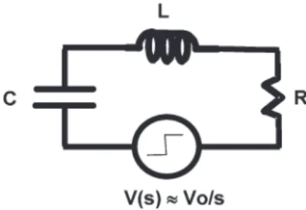
HE charged device model (CDM) test has, from its in-ception in the late 1980s, been considered essentially a discharge of a capacitor through series resistance and in-ductance to create an ESD current, much as pictured in the circuit model of Fig. 1. Early in CDM tester and standard development, it was recognized that the “3-capacitor model” [1] collapses to a single equivalent capacitor for the sake of simplified modeling. Much work has aimed at transforming tester properties into resistance–inductance–capacitance (RLC) parameters for a reasonable fit to measured waveforms, but such work has forced recognition of interaction with the CDM tester chassis ground, with a resulting “5-capacitor model” (plus one more inductor) and more complicated modeling [2]. But more recently, CDM tester manufacturers have removed or weakened the chassis ground interaction, and CDM waveforms over a wide range of calibration target and package sizes can be fit better than ever using simple RLC models.The s-domain current function for Fig. 1 is
I(s) = CV0
LCs2+RCs+1. (1)
s =σ+ jω, and the polesp1,2are such that
p1,2=ω0(−D±
D2−1) (2)
where ω0=1/
√
LC,D=ω0RC/2 and is commonly called
the damping factor [3]. The waveform will be a damped sinusoid (D<1), with a complex conjugate pole pair, or a
Manuscript received January 10, 2014; accepted March 11, 2014. Date of publication April 8, 2014; date of current version September 2, 2014. An earlier version of this paper appeared at the 35th Electrical Overstress/Electrostatic Discharge Symposium, Las Vegas, NV, USA, September 8–13, 2013, paper 9A.1.
T. J. Maloney is with Intel Corporation, Santa Clara, CA 95054 USA (e-mail: [email protected]).
N. Jack is with Intel Corporation, Hillsboro, OR 97124 USA (e-mail: [email protected]).
Color versions of one or more of the figures in this paper are available online at http://ieeexplore.ieee.org.
Digital Object Identifier 10.1109/TDMR.2014.2316177
Fig. 1. Two-pole RLC model of CDM pulse.
double exponential (D>1). Smaller components tend to be underdamped in CDM because D decreases with capacitance.
This paper will introduce a quick and effective way of selecting the R, L, and C circuit elements, as in Fig. 1, that aim to fit CDM waveforms as well as possible in a special way. The JEDEC/ESDA CDM committee, Industry Council on ESD Target Levels, and numerous EOS/ESD Symposium authors have long focused on the first half-cycle (or first peak) of the waveform because that is where the highest stress occurs, and its properties heavily influence device destruction. We will use two little-known mathematical properties of the two-pole circuit to fit peak current (Imax) and charge under the first peak(Qfp)exactly, while also accounting for ringing (if there
is undershoot) and other details of the waveform. The non-iterative calculation is simple enough to be deployed on an Excel spreadsheet, allowing waveforms to be characterized in mere seconds once the digital waveform is accessed. The result is guaranteed to fit Imax andQfpprecisely.
Using this powerful analytical method, it becomes much eas-ier to review the available data on CDM testers with elements such as series resistors, dielectric thickness variations, ferrites in the probe casing, and the effective resistance of the air spark as other parameters are varied. This paper will first describe the essentials of calculating R, L, and C for a given waveform, then will examine circuit element trends in various experimental ex-amples. With the insights that emerge, it is possible to envision and simulate new CDM tester configurations that could become an acceptable revised test standard.
II. RLC CALCULATIONS
A. Ideal Measurement Conditions
At first we will consider ideal measurement conditions, where the finite bandwidth of the measurement channel has negligible effect on the waveform. In the next section, we show how to check that the bandwidth effect is indeed negligible, or quantify minor adjustments to the data.
The general outline of the RLC calculation is shown in Fig. 2, where we start with measured waveform properties like
Fig. 2. Flow of RLC calculation forD<1, with Req, Leq, and Co corre-sponding to quantities in Fig. 1.
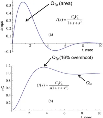
Fig. 3. (a) Computed waveform and (b) integrated waveform showing 16%
overshoot of the final charge forD =0.5; s in GHz.
charging voltageV0, first peak chargeQfp, final chargeQa(=
C0V0and peak current Imax, and use them to derive equivalent
R and L, which we’ll now call Req and Leq. Along with familiar relations like CV= Q andV =IR, we are going to need two rather obscure properties of the two-pole RLC circuit for extraction of the equivalent circuit from the waveform. The first applies to the smaller devices, forD<1, where we note the ratio ofQfptoQa, which can be shown (see Appendix A)
to depend entirely on damping factor D
Qf p
Qa
=1+ exp
−π√ D 1−D2
, D <1. (3)
Thus the ratio allows immediate calculation of D.
Fig. 3(a) shows what we mean by Qfp(= V0Cmax) for a
computedD =0.5,ω0=1 GHz, and 1 nC of charge Qa, while
Fig. 3(b) integrates that waveform, showingQfpat the peak. As
D approaches 1 or becomes greater than 1 for the larger CDM targets, the integrated charge due to undershoot becomes small to nonexistent, so this ratio method becomes ineffective. But at that point the centroid method [4] becomes less sensitive to
Fig. 4. Behavior of CDM Imax current function g(D), showing fraction of
V0/R reached.
undershoot effects and can better help to find D. We will return to that topic.
Clearly we are closing in on exactly capturing the first peak charge Qfp, one of our important quantities. The other one,
Imax, can be used to determine Req now that we know D, because it can be shown that
Imax=
2V0
Req
Dexp
− D
|1−D2|tan(h)
−1
|1−D2|
D
(4)
as discussed in Appendix B. The hyperbolic arctangent of (4) applies toD>1. As in Appendix B, the coefficient ofV0/Req
is a function g(D) that goes from 0 to 1, asD→ ∞is the well-known one-pole RC decay with current att =0+of V0/Req.
Fig. 4 shows the behavior of g(D).
At this point we have pegged Req to Imax and D toQfp, and
have foundC0from total charge, so Leq is determined from the
definition of D (Fig. 2) and we have a complete RLC model, one guaranteed to match the peak current Imax and the first peak chargeQfp.
B. Oscilloscope Bandwidth Effects
A previous paper by Maloney and Daniel [3] examined the filter function of an oscilloscope used to measure CDM wave-forms and reviewed previous related work by Mittermayer and Steininger (M-S) [5]. The previous work by M-S was confirmed in [3], and favored the pseudo-Gaussian two-pole model of the oscilloscope impulse response, with D =1/√2≈0.707. The poles of the filter function are as in (2), having equal real and imaginary parts, and withω0=2πf0, wheref0is the
3 dB rolloff frequency. Thus in the s-domain, an observed CDM event is described as
I(s) = CV0 1+√ω2
0s+
s2
ω2 0
(1+RCs+LCs2)
. (5)
hazards [6]. The routines for deconvolution of raw waveform data in [6] were not very successful, so we looked elsewhere.
It is possible to do Heaviside inversion of (5) into the time domain and examine it (and its derivative and integral, to find Imax andQfp) for sensitivity toω0 or 1/ω0. The problem is
that I(t) and related functions explode into expressions with dozens of terms, with expressions having powers of up to 4 or 5 in(1/f0), exponentials involvingf0, and such. Asf0goes up,
everything vanishes and the simple expressions of Section II-A are recovered, as expected, but it is not numerically accurate to simplify I(t) in customary ways, even for fairly highf0. It is
much more accurate to do direct convolution of pairs of two-pole functions as in (5) and mark the trends, even with some loss of generality.
The CDM waveforms with the sharpest peaks and highest ω values come from the smallest components and calibration targets, with low C and therefore damping factor D that is almost always less than one, underdamped. It is this collection of parts that centers aroundD =1/√2 (as discussed in a later section) and where the mathematics of convolution is not very sensitive for cases in the range of 0.5<D<1. Therefore, we focused on convolving pairs of normalized two-pole functions withD =0.707 and scaled values ofωin order to deduce some general trends.
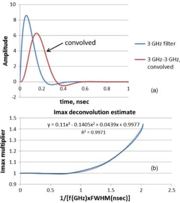
As an example, consider the case of a 3 GHz filter function convolved with itself, as in Fig. 5(a) (sometimes CDM wave-forms do indeed look like 2-pole impulse functions). The result-ing simulated 3 GHz scope waveform is shown, havresult-ing its Imax at about 73% of the real waveform. Thus when we see such a waveform, we should anticipate a higher Imax, with a multiplier of 1.367. Clearly it is desirable to use a higher frequency scope with such a fast waveform, but with measured FWHM (full width at half-maximum, also called Td) of 169 psec, this waveform is very fast. Because FWHM has been part of CDM standard measurements for decades, we are using it to present the estimated Imax multiplier, as in Fig. 5(b). The multiplier is plotted against a pure number, the reciprocal of the scope frequency f (GHz) times the FWHM (nsec). Our 1.367 number is toward the right-hand end(x≈1.98), and it is really not good to anticipate more than 40% increase in the ultimate Imax, so we halted calculations there. The cubic equation as shown fits the curve remarkably well, although there should be a vertical asymptote aroundx =2.78—again, this is approxi-mate, estimated behavior given a typical value of D. The true lesson is thatfor any scope with 3 dB bandwidth of f GHz, it appears we can be very confident of Imax for values of
FWHM=1/fnsecandabove. Small corrections can be made
using the cubic equation as in Fig. 5(b). These simple rules should apply to our familiar and most challenging combinations of CDM waveform and oscilloscope, wheref≥1 GHz and the
Fig. 5. (a) Two-pole impulse function (3 dB bandwidth of 3 GHz), and convolution of that function with itself, showing decline of Imax to∼73%. (b) Curve derived from many such convolutions, with Imax multiplier y inversely varying with scope bandwidth f and Td=FWHM.
CDM waveform is underdamped and fast. Using FWHM also avoids the occasional “arc extinction” phenomenon, where the waveform fails to cross zero even though it is headed there.
A similar study ofQfp revealed very little change over the
same range, with the multiplier still between 0.98 and 1.0 at x =2.03, where the Imax multiplier reached 1.45. Because of the approximations involved, it is probably best to adjust only Imax, notQfp, before calculating the RLC.
The curve and equation of Fig. 5(b) was applied to some Orion2 CDM tester data comparing both 1 and 8 GHz scopes on the JEDEC large and JEDEC small calibration targets. The large JEDEC target, with FWHM in the 625–700 psec range, presented x≈0.2, and negligible correction, for the 8 GHz data but for 1 GHz,x≈1.5 and the correction should be in the 10–13% range. This was found to be exactly the case, with the predicted value of 8 GHz Imax from 1 GHz data usually within 1% and often far better. The small target’s FWHM ranged from 375–465 psec and the predicted correction for 1 GHz data was overestimated, in the 50–60% range instead of the measured 40%. But at a typical value of x =2.25 or more, this is out of range of Fig. 5(b) and not recommended for serious RLC calculations. The small JEDEC CDM target deserves at least a 2–3 GHz oscilloscope.
III. EXPERIMENTALRESULTS
A. C0Versus Package Size
Fig. 6. Effective CDM capacitance versus metal target size. JEDEC circular targets are the first and third nonzero points, while P4 and P6 circular targets are the second and fourth.
Fig. 7. Req on Intel Orion2 tester follows slope-intercept form for the four targets in Fig. 6. Inductance varies as shown.
know a worst caseC0 (effective capacitance from integrated
“fast” current), the size trend with metal target area should be sufficient. Packages of similar area that add dielectric should have smallerC0, and a single Vss pulse could yield its exact
C0value. The trend ofC0with target size within our range of
interest of sizes is empirically simple, as seen in Fig. 6 with a square root dependence on area. Values for 250 V nearly coincide with 500 V, as expected. Dielectric was the standard JEDEC 15 mils (0.381 mm), as is the case in all this work unless otherwise stated.
C0 is a series-parallel combination as shown in the 3-cap
model [1], [2], and calculations including fringing capacitance confirm this trend. We now can correlateC0with package size.
B. Standard JEDEC Tester
When 8 GHz waveforms from standard JEDEC testers were analyzed as in Section I, we found, remarkably, that resistance goes up as target size decreases, but in orderly fashion (Fig. 7), due to a constant slope and non-zero intercept. When tau= ReqC0 is plotted against C0, it appears that we can predict
Req= [20.6+68.7 psec/C0(pF)]ohms for 250 V.
The slope-intercept fit was also found at 500 V (Fig. 8), but with a higher slope (27.5 ohms) and not much smaller intercept (56.8 psec). This was over an even wider range of capacitance (i.e., metal target size) and at a different company. Measurements on four targets at Intel gave 27.8 ohms at 500 V, closely agreeing with Fig. 7. The inductance Leq (Figs. 6 and 7) completes the model and varies as shown. There is slightly higher average Leq (11.9 nH) for 500 V, plus a downward trend
Fig. 8. Req on Orion2 JEDEC tester also follows slope-intercept form, using seven targets of various sizes. Inductance varies as shown. Data used with permission and provided by M. Johnson, Texas Instruments.
Fig. 9. Measured and 2-pole waveforms for large JEDEC target in Intel Orion2 tester, 500 V.
withC0that could be traceable to spark rise time. With these
trends in Req, Leq, and C0, plus the prediction of C0 from
package size, we have a way to predict JEDEC waveforms and their properties over a wide variety of packages.
Fig. 9 shows an example of how well the modeling method fits a measured (8 GHz scope) waveform. The Fig. 9 waveform was taken on an Orion2 JEDEC tester at 500 V and uses parameters of Req=28.6 ohms, C0=16.28 pF, and Leq=
11.69 nH in order to match Imax andQfpexactly.
C. FFPA Trials
In recent times, Intel participated in the efforts of the JEDEC/ESDA CDM standards committee members (including Analog Devices and two locations at Texas Instruments) to vary the thickness of the dielectric over the field plate from 14 to 59 mils (0.36–1.5 mm) for the small and large JEDEC targets. 8 GHz data at around 500 V on modified testers without a ferrite (FFPA or ferrite-free probe assembly) were acquired and analyzed. Thicker dielectric, it was hoped, would lower Imax for our desired test voltages in the absence of the ferrite, and thus make testers more reproducible. However, the absence of a ferrite seemed to lower the 510 V Req slope somewhat (20.6 ohms; see Fig. 10) and lowered the Leq to the ranges shown, averaging 3.5 nH, much as calculated for the metal probe itself. But the tau vs.C0plot correlated extremely well,
Fig. 10. Req on RCDM3 tester with dielectric thickness variation for two JEDEC targets; lowerC0with thicker dielectric. Average inductance Leq is given for each group. Data from JEDEC/ESDA CDM standards committee; used with permission.
Fig. 11. Req tau plot for 25 ohm termination on Orion2 CCDM test head, showing 48.9 ohm slope for both 250 and 500 V. Average inductance Leq is 11.62 nH.
Imax currents. A similar effect with the low Leq was seen with a CDM fixture having 10 ohm resistance to ground (instead of 1 ohm) from the probe—even with 10 ohms added to the spark resistance, Imax currents were off-target as far as preserving the JEDEC CDM legacy [7]. Some other way of approximating the JEDEC CDM test was needed.
D. Air Spark and 25 ohm Series Resistance
The Orion2 CCDM (contact CDM, also called CDM2 [8]) test head can also be used in air spark mode, although this adds 50 ohms to the air spark. The CDM discharge waveform ends up having much charge in a long, extended tail, apparently because the spark breaks up in its later stages due to the weaker driving force of the 50 ohms. But with a 25 ohm load from probe to ground instead of 50 ohms, these effects were much reduced and the results much closer to reproducing the JEDEC CDM legacy.
The 25 ohm termination of the CCDM test head probe was achieved with an SMA tee on the test head, terminating one branch with 50 ohms and the other with a 50 ohm cable to the oscilloscope 50 ohm input and attenuator as usual. This places the 25 ohm load at the end of a 2–3 cm 50 ohm coaxial line inside the CCDM test head, an inductive termination that may or may not be desired.
Fig. 11 shows that the 25 ohm load adds an average of 25 ohms to a spark of about 24 ohms for both test voltages,
Fig. 12. Waveform and 2-pole fit for small JEDEC target on 25-ohm-terminated CCDM fixture with air spark, 500 V.C0=4.57 pF,D =0.4606,
ω0=4.007 GHz, so Req=50.3 ohms, Leq=13.6 nH.
Fig. 13. 25-ohm results for two voltages and JEDEC for 250 V, plotted in the plane of Imax and Qfp. JEDEC data from M. Johnson, Texas Instruments.
and that Leq is about 11.6 nH. This is in the range of the ferrite-equipped JEDEC test head Leq, with extra inductance evidently due to the mismatch of the embedded 50-ohm line. An example of waveform match to the RLC fit is shown in Fig. 12.
The true test of the 25-ohm scheme’s utility is comparison with the JEDEC CDM tester for critical parameters like Imax andQfp, as in Fig. 13. The same four targets as in Figs. 5–7
were used. The red arrows show the presumed linear path in Imax-Qfp space that would be traversed going from 250 to
500 V for the 25-ohm test. It is clear that the exact Imax andQfp
conditions of 250 V JEDEC cannot be reproduced by 25 ohms for all target sizes. However, Imax or Qfp can always be hit
by varying precharge voltage to somewhere between 250 and 500 V, depending on target size. For a least-squares fit to both Imax andQfp, one would first normalize the chart scales for
each target JEDEC value (triangles in Fig. 13), and adjust for any weighting factors being applied to Imax and Qfp.
Then drop a perpendicular from the target triangle to the line connecting 250 to 500 V 25-ohm values; the associated voltage represents the closest approach to the target values of Imax andQfp.
E. CCDM or CDM2
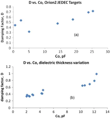
Fig. 14. Damping factor trends for (a) JEDEC targets as in Fig. 7 (data from M. Johnson, Texas Instruments) and (b) FFPA dielectric thickness data as in Fig. 10 (data from JEDEC/ESDA CDM committee). D clusters around mildly underdamped values.
ordinary use (relay and 50 ohm cable) showed Req≈55 ohms for both targets and Leq≈3.9 nH for the large target, where little influence due to relay spark rise time is expected (small target Leq was 6.45 nH). In any case, under these Z-matched and no-air-spark conditions, the fixture shows the expected resistance and Leq consistent with no ferrite. A 25 ohm CCDM test might give even closer agreement with JEDEC than the 50 ohm. Prospects for mapping multiple targets and voltages for comparison with JEDEC, as in Fig. 13, are good.
IV. DISCUSSION: DAMPINGFACTOR
TRENDS ANDSPARKBURNRATE
Another way to examine the variation of Req and Leq asC0
varies is to look at how D varies. We might expect from the definition of D (in Fig. 2, for example) for it to increase as the square root ofC0, but that is not really the case.
Fig. 14 shows two examples, with data from earlier figures, of damping factor D vs. C0, and the tendency of D to settle
around a mid-range of mildly underdamped values. This is clearest in Fig. 14(b), where the break between large and small JEDEC targets was why we could not acquire data in theC0
range where the plateau seems to be. Even so, Fig. 14 suggests that D is compressed into a mid-range and may “break out” to higher or lower values at high or low capacitance, but clearly does not follow √C0, as would be the case if Req and Leq
remained constant. Why might this be?
The answer could be in the physics of the electrostatic spark plasma, which after all has a “resistance” based on its ability to create heat, light, sound, excited atoms and molecules, etc., in a short period of time, with energy supplied by the
Fig. 15. (a) Dissipation rate versus time (in√LC units) for three values of damping factor D. For each curve, the normalized initial field energyAp=1. (b) Remaining fraction of electric and magnetic field energy versus time for optimized valueD =1/√2; dissipation timeAe=√2 time units, lower than any other D.
collapsing fields. The total field energy goes down as the plasma burns energy, but as the event progresses, the field energy is partitioned between electric and magnetic fields. The current i(t) drains the electric field initially stored in C, but is limited by magnetic field storage proportional to L. We therefore expect the RLC network’s time constant √LC to determine how fast the field energy can be dissipated.
For low damping factor D approaching zero, the 2-pole RLC circuit rings for a long time and does not dissipate field energy very fast compared with time scale√LC. The same is true of highD1, where the capacitor discharges slowly. There must be an intermediate D at which the field energy burns off as fast as possible, on the order of time scale√LC. That D is 1/√2, as shown in Appendix C, if the energy decay time is measured by integrating the (normalized) remaining field energy over time, starting with the beginning of the spark discharge.
Fig. 15 shows what happens with power dissipation (i2(t)Req)and remaining field energy versus time, where time
is in normalized units of√LC as described in the appendices, for three values of D. The area Ap in Fig. 15(a) is the same
for all D because it is the initial field energy C0V20/2,
nor-malized to one. But there are subtle differences among curves for D =0.5,0.707. . ., and 1.0, such that the first moment (centroid) of the middle one, for D =0.707. . ., is minimum (see Appendix C). This quantity (in normalized time units) is the areaAein Fig. 15(b) and is 1.414. . .or
√
2 forD =1/√2, while it is 1.5 for D =0.5 and D =1. Thus the maximum plasma burn rate, for fixed resistance, occurs whenD =1/√2 orR=2L/C.
proachesD =1/ 2 with a time constant of 1 (meaning that D<0.7 for the bulk of the pulse), we get a time constant (area Ae) of only 1.39 time units. This trial was inspired by finding
thatD≈0.55 produces maximum power dissipation at Imax. The optimal solution, if unique, is not yet known but is likely to be better than 1.39. But any mathematically ideal solution also has to merge with “reasonable” physical conditions in the plasma. For example, the spark initiates through ionization and the resistance comes down from infinity in a short period of time [9], although sometimes we account for this in the circuit model by introducing extra poles to describe the rise time of the spark [10]–[12]. While the spark rise time is believed to be only tens of picoseconds, maximum burn rate of the field energy may describe the bulk of the nanosecond-scale CDM discharge time. We now discuss why this could be reasonable.
The idea of minimizingAein Fig. 15(b) suggests some kind
of Least Action Principle as in Lagrangian mechanics [13], as Action is defined as Energy×Time. The integral Ae of field
energy over time is indeed a minimum(√2)for D =1/√2, as discussed above, when D(t) is constant, and is known to be lower for some D(t). But it is more intriguing to consider
why this maximum burn rate of field energy might happen to the spark plasma: Maximum burn rate should also mean a maximum rate of increase of entropy in the system, as the spark plasma produces heat. The spark plasma system, while certainly not in equilibrium, does evolve toward a most likely state, in accordance with the definition of entropy in statistical mechanics. It is thus not surprising to see a spark plasma adopt a maximum burn rate when that rate is not constrained by other processes in the plasma. Those processes, like the spark rise time discussed above, may often be fast enough to allow very close to the maximum burn rate for the nanosecond-scale CDM event.
The concept of least action and of maximum entropy in dissipative Lagrangian systems has been examined over the last century or more (Lord Rayleigh is often cited on dissipation) and is still a subject of discussion and research. One recent author [14], [15] has even produced work on least action and its ties to maximum entropy and stochastic mechanisms in systems in and out of equilibrium. We will not attempt to resolve any of these long-standing controversies. But our data in Fig. 14 do offer something for the theorists to consider—a possible example of a dissipative system that is driven by easily understood physical principles to behave in a certain quantifiable way. Fig. 14 suggests that if the physical conditions are right—plasma processes on a much shorter time scale than √
LC for example—the damping factor D assumes values near those associated with maximum burn rate of the field energy, for a large range of capacitanceC0.
also inspiring explanations of many previous observations. We were very inspired by certain previous CDM studies [2], [16] and yet noted that the present methods offer significant new benefits to contemporary CDM workers who undertake modeling:
1) CapacitanceC0 is likely to correlate to the square root
of area for comparable objects, e.g., the metal calibra-tion targets and packages with similar amounts of extra dielectric.
2) The variation of equivalent resistance Req withC0is best
studied by plotting ReqC0vs.C0to give a slope-intercept
linear form. The linear fit, at least for metal targets, can have an astoundingly high correlation coefficient (R2=
0.997 in one case) and has been observed with and with-out ferrites in the CDM fixture. Variations in equivalent spark resistance thus became much less mysterious. 3) Inductance Leq has some scatter over the full range ofC0
values for a given configuration, but is usually stable, and the effect of a ferrite in the CDM fixture—raising Leq and Req—is easily observed.
4) Trends in the damping factor(D =ReqC0/[2√LeqC0]) are easily tracked and plotted, given that all the new calculations can be captured on an Excel spreadsheet after a few key parameters are extracted from each wave-form. Over a considerable C0 range, D was seen to be
compressed toward values indicating maximum possible dissipation rate of field energy by a resistor. We think D should be watched for further revealing evidence. The use of a 25-ohm series resistance in a ferrite-free probe assembly was fairly successful in reproducing JEDEC-like CDM conditions as long as plate voltage could be varied to match JEDEC Imax and first peak charge Qfp. This was
done with the air spark in series, giving Req≈50 Ω. The same 25-ohm coaxial resistance could possibly be used in CDM2/CCDM [6] to simulate the air spark reproducibly and achieve even closer agreement with JEDEC waveforms, given also that there would be a mismatched 50-ohm line segment in the CDM2/CCDM fixture that could provide extra equivalent inductance. These continuing studies suggest that a more repro-ducible CDM test could be achieved without much departure from the JEDEC CDM legacy.
APPENDIXA FIRSTPEAKCHARGE
ForD<1, we start with the expression for CDM current for Fig. 1 as recorded by [2] from many textbooks, including [17]
i(t) = V0 ωL·e
where
a= R
2L, ω= ω
2
0−a2 (A2)
andω0=1/
√
LC, as below (2), earlier. In terms of D andω0
i(t) =2V0 R ·
D √
1−D2e
−ω0Dt·sin(ω 0
1−D2t)
=√V0ω0C 1−D2e
−ω0Dt·sin(ω 0
1−D2t). (A3)
From standard tables, the current integrated from 0 to∞isQa=
CV0, as expected. Note also that time can be normalized to units
of 1/ω0, with simpler expressions if we allowω0=1. To find
Qfp, the charge under the first peak or first half cycle, we want
Qf p=
CV0
√ 1−D2
π √
1−D2
0
e−Dt·sin(1−D2t)dt. (A4)
Again with the help of standard integral tables, this is
Qf p=
CV0
√ 1−D2
e−Dt−√1−D2cos(√1−D2t)
D2+1−D2
√π 1−D2
0
=CV0
1+ exp
−π√ D 1−D2
(A5)
in accordance with (3).
APPENDIXB PEAKCURRENT
The CDM current for the circuit in Fig. 1 will peak at the first occurrence of di(t)/dt=0. Differentiating (A3) forD<1 means that Imax occurs when
−ω0Dsin(ω0
1−D2t 0)
+ω0
1−D2cos(ω 0
1−D2t
0) =0, or (B1)
tan(ω0
1−D2t 0) =
√ 1−D2
D . (B2)
Again, using normalized time units and allowingω0=1 will
not affect the answer. Substituting the peak current timet0back
into (A3), we get
Imax=
2V0
R Dexp
−√ D 1−D2tan
−1
√
1−D2
D
(B3)
in accordance with (4) forD<1. ForD>1, a similar derivative is sought, as there is a sinh expression for the current replacing sin, tanh for Imax, and D2-1 replacing 1-D2, still a positive
quantity. Note that Imax is always a fraction g(D) ofV0/R
Imax=
V0
Rg(D)
g(D) =2Dexp
− D
|1−D2|tan(h)
−1
|1−D2|
D
. (B4)
At D =1, i(t) is of the form te−t and g(1) =2/e. g(D) is
plotted in Fig. 4 of the text.
APPENDIXC
MAXIMUMBURNRATE OFFIELDENERGY
Power dissipation in the CDM spark isi2(t)R, and its integral
over time will be equal to the initial field energyQ2
a/2C. This
integral can also be used to show the remaining fraction of field energy, electric and magnetic, versus time. As described in the text, we are interested in the value of R (proportional to D) giving the fastest dissipation of the field energy, and will measure that speed with the time integral of the remaining fraction of field energy. We would like to minimize this field collapse time given a choice of L and C, and for simplicity, we will consider a fixed D. We expect some kind of time-variant D (i.e., R) to give the lowest value of field collapse time, but will not attempt a rigorous global solution.
Starting with (A1) for i(t) and again (since L and C are fixed) using normalized time units of 1/ω0, we have
P(t) =i2(t)R∝De−2Dt·sin2(1−D2t)
∝e−2Dt
1−cos(21−D2t). (C1)
Proportionalities are sufficient since we simply want to examine time dependence on D and minimize the decay time of the field energy, found by integrating P(t) and noting the rise time. The last expression in (C1) converts to the s-domain when we consult a table of Laplace Transforms [18]
P(s)∝ 1 s+2D −
s+2D (s+2D)2+4−4D2
= A
1+2sD −
B1+2sD
1+Ds+s42 (C2) where A =1/2D, B = D/2. In the s-domain, the dissipated energy E(s) = P(s)/s, so the essentials are in (C2). To find the rise time of consumed energy E(s) (equal to field collapse time), we consider the Elmore Delay of (C2) by finding the s-coefficient of its normalized series expansion, as done in [3], [4] and many other references. After some manipulation, (C2) becomes
P(s)∝
(A−B)
1+
AD−B/D A−B
s+O(s2)
1+D+21Ds+O(s2) +· · · . (C3)
However, note that AD-B/D=0. Thus our time constant is the s-coefficient of the denominator
τe=D+
1
2D (C4)
which is minimum (√2 time units) atD =1/√2=0.707. . .. Note also that τe=1.5 atD =0.5 andD =1, and that D =
1/√2 is their geometric mean. Thus we have proven that the slightly underdamped D =1/√2 or R=2L/C produces “maximum burn rate” of the field energy by a fixed resis-tance. Curiously, this same function and D-factor (whereD = √
(1-D2), with quality factor Q =1/2D= D) has been called
REFERENCES
[1] R. Renninger, M.-C. Jon, D. L. Lin, T. Diep, and T. L. Welsher, “A field-induced charged-device model simulator,” inProc. EOS/ESD Symp., 1989, pp. 59–71.
[2] B. C. Atwood, Y. Zhou, D. Clarke, and T. Weyl, “Effect of large device capacitance on FICDM peak current,” inProc. EOS/ESD Symp., 2007, pp. 273–282. [Online]. Available: http://ieeexplore.ieee.org/stamp/stamp. jsp?tp=&arnumber=4401763
[3] T. J. Maloney and A. Daniel, “Filter models of CDM measurement channels and TLP device Transients,” inProc. EOS/ESD Symp., 2011, pp. 386–394. [Online]. Available: http://ieeexplore.ieee.org/stamp/stamp. jsp?tp=&arnumber=6045570
[4] T. J. Maloney, “HBM tester waveforms, equivalent circuits, and socket ca-pacitance,” inProc. EOS/ESD Symp., 2010, pp. 407–415. [Online]. Avail-able: http://ieeexplore.ieee.org/stamp/stamp.jsp?tp=&arnumber=5623761 [5] C. Mittermayer and A. Steininger, “On the determination of dynamic errors for rise time measurement with an oscilloscope,” IEEE Trans. Instrum. Meas., vol. 48, no. 6, pp. 1103–1107, Dec. 1999. [Online]. Avail-able: http://ieeexplore.ieee.org/stamp/stamp.jsp?tp=&arnumber=816121 [6] R. de Levie, MacroBundle12, May 2012. [Online]. Available: http://www.
bowdoin.edu/~rdelevie/excellaneous/#downloads
[7] A. Righter, T. Welsher, M. Farris, M. Johnson, S. Ward, M. Dekker, T. Maloney, R. Ashton, L. G. Henry, T. Meuse, J. Barth, E. Grund, T. Smedes, and P. Ngan, “Progress towards a joint ESDA/JEDEC CDM standard: Methods experiments, and results,” inProc. EOS/ESD Symp., 2012, pp. 32–41. [Online]. Available: http://ieeexplore.ieee.org/stamp/ stamp.jsp?tp=&arnumber=6333283
[8] R. Given, M. Hernandez, and T. Meuse, “CDM2—A new CDM test method for improved test repeatability and reproducibility,” in
Proc. EOS/ESD Symp., 2010, pp. 359–367. [Online]. Available: http:// ieeexplore.ieee.org/stamp/stamp.jsp?tp=&arnumber=5623751
[9] R. G. Renninger, “Mechanisms of charged-device electrostatic dis-charges,” inProc. EOS/ESD Symp., 1991, pp. 127–143.
[10] T. J. Maloney, “Easy access to pulsed Hertzian dipole fields through pole-zero treatment,”IEEE Electromagn. Compat. Soc. Newsletter, pp. 34–42, Summer, 2011. [Online]. Available: http://ewh.ieee.org/soc/emcs/acstrial/ newsletters/summer11/index.html
[11] T. J. Maloney, “Antenna response to CDM E-fields,” inProc. EOS/ESD Symp., 2012, pp. 268–278. [Online]. Available: http://ieeexplore.ieee.org/ stamp/stamp.jsp?tp=&arnumber=6333315
[12] T. J. Maloney, “Pulsed Hertzian dipole radiation and electrostatic dis-charge events in manufacturing,” IEEE Electromagn. Compat. Mag., vol. 2, no. 3, pp. 49–58, 3rd Quart., 2013. [Online]. Available: http:// ieeexplore.ieee.org/stamp/stamp.jsp?tp=&arnumber=6623294
[13] H. Goldstein, Classical Mechanics. Reading, MA, USA: Addison-Wesley, 1950.
[14] Q. A. Wang and R. Wang, Is it Possible to Formulate Least Action Prin-ciple for Dissipative Systems? Jul. 2012. [Online]. Available: http://arxiv. org/abs/1201.6309v5
[15] Q. A. Wang, From Virtual Work Principle to Least Action Principle for Stochastic Dynamics, Apr. 2007. [Online]. Available: http://arxiv.org/ftp/ arxiv/papers/0704/0704.1708.pdf
Timothy J. Maloney(M’73–SM’84–F’08) received the S.B. degree in physics from the Massachusetts Institute of Technology, Cambridge, MA, USA, in 1971; the M.S. degree in physics from Cornell Uni-versity, Ithaca, NY, USA, in 1973; and the Ph.D. degree in electrical engineering from Cornell Uni-versity in 1976, where he was a National Science Foundation Fellow.
He was a Postdoctoral Associate with Cornell University until 1977, when he joined the Central Research Laboratory, Varian Associates, Palo Alto, CA, USA. At Varian Associates, he worked on III–V semiconductor photo-cathodes, solar cells, and microwave devices, as well as on silicon molecular beam epitaxy and MOS process technology, until 1984. Since 1984, he has been with Intel Corporation, Santa Clara, CA, engaged in integrated circuit electro-static discharge (ESD) protection, complementary metal–oxide–semiconductor latchup testing, fabrication process reliability, signal integrity, system ESD testing, and design and testing of standard IC layouts. He is currently a Senior Principal Engineer with Intel. He has received the Intel Achievement Award for his patented ESD protection devices, which have achieved breakthrough ESD performance enhancements for a wide variety of Intel products. He now holds 37 patents, with several more pending.
Dr. Maloney received Best Paper Awards for his contributions to the EOS/ESD Symposium in 1986 and 1990, was the General Chairman for the 1992 EOS/ESD Symposium, and received the ESD Association’s Outstanding Contributions Award in 1995. He has taught short courses at the University of California, Los Angeles, CA, USA; the University of Wisconsin—Madison, WI, USA; and the University of California, Berkeley, CA, USA. He is the coauthor of the book “Basic ESD and I/O Design” (Wiley, 1998).
Nathan Jack (M’12) received the B.S. degree (magna cum laude) in electrical and computer en-gineering from Utah State University, Logan, UT, USA, in 2007 and the M.S. and Ph.D. degrees in electrical and computer engineering from the Uni-versity of Illinois at Urbana-Champaign, Urbana, IL, USA, in 2009 and 2012, respectively.
He is currently an ESD/Latchup Reliability En-gineer with Intel Corporation, Hillsboro, OR, USA. While a student, he completed summer internships at Intel Corporation in Hillsboro, OR, and at IBM in Essex Junction, VT, both of which were in the ESD reliability groups. He also completed five summer internships at Micron Technology, Inc., Boise, ID, USA, of which two were in the ESD/Latchup R&D Reliability Group. His research interests include on-chip ESD protection and ESD test methods.