HIGH SPEED AND AREA EFFICIENT FPGA
IMPLEMENTATION OF FIR FILTER USING DISTRIBUTED
ARITHMETIC
1 K.G.SHANTHI, 2 N.NAGARAJAN
1
Associate Professor,Department of Electronics & Communication, R.M.K Engineering College, India. 2
Principal & Professor,Department of Computer Science, Coimbatore Institute of Engineering and Technology, Tamil Nadu, India.
E-mail: [email protected], [email protected]
ABSTRACT
In this paper, high speed and area efficient multiplier-less architecture for Finite impulse response filter (FIR) based on distributed arithmetic is presented. The proposed Lookup table less architecture for FIR filter uses the speed advantage of Carry save adder. A modification in the shift accumulator stage yields both high speed and area savings. Furthermore, Memory reduction is possible since there is no Lookup table of precomputed values and only based on the input value the needed coefficient values are calculated. The proposed LUT less architecture was implemented on a Xilinx FPGA device. Number of slices, minimum period and maximum frequency were the performance metrics obtained for different filter orders and the results prove that the proposed method yields higher speed and smaller area when compared with the existing LUT-less architectures.
Keywords:Finite Impulse Response Filter (FIR), Distributed Arithmetic (DA), Lookup Table (LUT), Carry Save Adder (CSA), Shift Accumulator (SA).
1. INTRODUCTION
In the recent years Digital signal processing (DSP) has created a major impact in the areas of digital communication, speech and image processing, adaptive filtering applications, satellite communication, wired and wireless communication, multimedia systems, biomedical instrumentation [1]. The increased daily use of digital technology has led to the development of improved algorithms and architectures to design the DSP systems with less power dissipation, higher speed performance and less area complexity. Several architectural solutions have been postulated by the research community to minimize the arithmetic complexities of the algorithms thereby reducing the overall area-delay-power requirements [2].
Finite impulse response (FIR) digital filters are key components used in many digital signal processing (DSP) systems because of their linear phase, stability and regular structure. Digital filters modify signal characteristics in time or frequency domain and are used in many DSP systems to perform signal preconditioning, filtering, interpolation etc [1]. For the past one decade, there has been a growing trend to implement DSP functions in Field Programmable Gate Arrays
(FPGAs) rather than on Application specific integrated circuits (ASIC) and DSP chips. The implementation on ASICs is not preferred due to high development costs and time-to-market factors. Sequential-execution architecture of programmable DSP processors prevents them from achieving the desired performance. FPGAs are preferred due to their high flexibility with the option to reconfigure, time-to-market, cost and performance [3].
The output y[n] of an N- tap discrete-time linear finite impulse response (FIR) filter is represented as
1
0
[ ] [ ] [ ]
N
i
y n C i x n i
−
=
=
∑
−(1)
manipulate the filter coefficients for the multiply operation. The first type is the conversion-based approach where
the
coefficients are transformed to other numeric representations so that the multiplications were implemented with adder/subtractors and shifters [4]-[5]. The second memory based approach which yields a faster output uses memories (RAMs, ROMs) or Look-Up Tables (LUTs) that store pre-computed values that can be readout for multiplication operation.Distributed Arithmetic is a bit-serial operation which performs the computation of inner product by a sequence of lookup table accesses followed by shift-accumulation operations of the LUT output to obtain the desired result as shown in figure 1.The advantage of FIR filters based on DA is that the time complexity depends only on the input word length and is independent of the order of filter (N). Croisier et al had proposed the DA algorithm for digital filter implementations in 1973[6]. The first detailed discussion of DA was given by Abraham Peled and Bede Liu in 1974 at the Arden House Workshop on Digital Signal Processing [7]. S.A.White [8] had given a detailed note on Applications of Distributed Arithmetic to Digital Signal Processing. A review of the various memory based architectures for the implementation of FIR filters was given by Shanthi et al [9].
The main drawback of DA method is that the memory size (2N) grows exponentially as the filter order N increases. With the use of offset binary coding(OBC) the memory size can be reduced by half to 2N-1 words [2], [8]. If a single term inside the LUT is relocated outside the LUT,
then the lower half of the LUT is mirrored version of the upper half of the LUT with only the signs reversed which results in reducing the LUT size from 2N−2 to 2 in Distributed arithmetic with Modified Offset Binary Coding (DA-MOBC) [10]. A LUT-less DA architecture can be achieved by recursive LUT reduction with multiplexers and ripple carry adders [11]. On-Line LUT-less DA architecture for FIR filter using tri-state buffers and carry look ahead adders (CLA) was proposed by Eshtawie et al[12]. Area-Efficient FIR filter design was proposed by Patrick Longa et al that rearranges the input sequence to implement a modified version of the shifter/accumulator stage [13].
To reduce the memory-size of DA-based filters several memory-partitioning and multiple memory bank approaches along with flexible multi-bit data access mechanisms were presented [8],[14]. One and two dimensional fully pipelined computing structures are presented for area-delay-power-efficient implementation of FIR filter by systolic decomposition of DA based inner-product computation [15]. FPGA realization of FIR filters for high-speed and medium-speed by using modified DA architectures were suggested by Jiafeng Xie et al., which made use of pipelined registers and pipelined shift adder tree [16].
This paper is organized as follows: Section 2 details the main concept of DA. Section 3 explains the new architecture for LUT-less DA based FIR filter. FPGA implementation and Comparison of performance metrics of the proposed architecture with the existing methods is detailed in section 4. Conclusion is presented in section 5.
Figure 1:LUT-Based Design Of A 4-Tap (N =4) FIR Filter Using DA b
1 x(n-3)
x(n-1) x(n-2)
x(n)
b 3
b 2
b 0
Input Signal Input Shift Register Unit
Look up table (2
N
=16 Word ROM)
b3 b2 b1 b0 Contents of ROM 0 0 0 0
0 0 0 1 0 0 1 0 0 0 1 1 0 1 0 0 0 1 0 1 0 1 1 0 0 1 1 1 1 0 0 0 1 0 0 1 1 0 1 0 1 0 1 1 1 1 0 0 1 1 0 1 1 1 1 0 1 1 1 1
0 C0 C1 C0+ C1 C2 C0+ C2 C1+ C2 C0 +C1+ C2 C3 C0+ C3 C1+ C3 C0 +C1+ C3 C2+ C3 C0 +C2+ C3 C1 +C2+ C3 C0+C1 +C2+ C3
Shift Accumulator unit
Accumulator
Shift right
+/-
S=1 for MSB
2. DISTRIBUTED ARITHMETIC (DA)
The input sample of the FIR filter is coded as B-bit 2’s complement binary number given by
B - 1
- j
i i 0 i j
j = 1
x = - x
+
∑
x
2
(2)Where xi, j ϵ {0, 1}, xi0 is the sign bit and xi, B-1 is the Least significant bit (LSB).Substituting (2) in (1) and changing the order of summations, the output can be expressed as
N -1 B -1
- j i i 0 i j
i= 0 j= 1
y[n ]= C -x + x 2
∑
∑
(3)N - 1 B - 1 N - 1
- j
i i 0 i i j
i = 0 j = 1 i = 0
y [ n ] = - C x + C x 2
∑
∑ ∑
(4)
For a given set of coefficients Ci(i = 0, 1, 2,…., N − 1), the terms in the brackets may take one of 2N possible values that can be precomputed and stored in a LUT that can be read out from the ROM using the N bit sequence {xi,j for 0 ≤ i ≤ N} as address bits. These intermediate results are accumulated in B clock cycles to produce one filter output y[n].
Conventional LUT based design of a 4-tap (N =4) FIR filter shown in figure 1consists of three units: Input Shift Register Unit, Look up table unit, and Shift Accumulator unit. The LUT contains all 16 possible combination sums of the filter weights C0, C1, C2, and C3. The input shift registers stores four consecutive input samples(x[n-i],i=0,1,2,3). The concatenation of rightmost bits of the shift registers becomes the address of the LUT. The shift register is shifted right at every clock cycle. The corresponding LUT entries are read out and accumulated in B consecutive times to generate the output y[n]. The sign bits {xi0} are the last bits that simultaneously arrive in a clock period called the "sign-bit time”. During the sign-bit time the control signal S = 1, otherwise S = 0.
3. PROPOSED ARCHITECTURE
3.1 LUT -Less DA Architectures
A LUT-less DA based architecture using multiplexers and ripple carry adders [11] is presented in figure 2 for comparison of performance with the proposed architecture explained in the next subsection. According to Yoo et al [11], the lower half of LUT as shown in figure 1whose addresses have a ‘1’ in the MSB location is the upper half of LUT whose addresses have a ‘0’ in the MSB location and C3 term. Therefore LUT size can be reduced by half with an additional 2:1
[image:3.595.312.524.231.428.2]multiplexer and a full adder. By recursive LUT reduction technique, a final LUT -less DA architecture was obtained which proved to be better in terms of hardware requirements compared with the earlier realizations of FIR filters [8], [10]. For an N tap filter, N-1 number of ripple carry adders was used in the design. The ripple carry adder requires n full adders where n represents the number of bits in each coefficient.
Figure 2:LUT-less DA Based Design of an 8-Tap FIR Filter Using Multiplexers and Ripple Carry Adders
[image:3.595.91.284.257.320.2]Another LUT-less DA based architecture (figure 3) presented by Eshtawie et al [12] uses tristate buffers and carry look ahead adders (CLA)
Figure 3:LUT-less DA Based Design Of an 8-Tap FIR Filter Using Tristate Buffers and Carry Look Ahead
Adders
Sign
Control Y(n) S (1 for MSB)
Tristate buffer b7
b6 b5 b4 b3 b2 b1 b0
C7
C6
C5
C4
C3
C2
C1
C0
Input Input
Shifter +/-
Accumulator
>>1 Carry
Look Adder Tree 0
0
b7 b6 b5 b4 b3 b2 b1 b0
C7
C6
C5
C4
C3
C2
C1
C0
+ +
0
0
0
0
0
0
+
+ +
+ +
Input Input Shifter
Y (n)
Sign Control S (1 for MSB)
>>1 +/- Accumulator RCA
[image:3.595.311.508.499.705.2]that has O(log n) delay, n being the number of bits in the operands to be added. Computation time of CLA adder is lesser than that of RCA for it calculates carry signals based on the input signals. Ripple carry adders are very slow adders having O(n) delay where the carry signal propagates through all the full adders to generate final output carry. Hence architecture [12] yielded a higher speed when compared with Yoo’s design. A comparison of various adders in terms of speed, power and area is presented by Uma et al [17].
3.2 Proposed LUT -Less DA Architecture
[image:4.595.68.281.335.519.2]The proposed method presented in figure 4 replaces the Ripple carry adder tree of figure 2 by a carry save adder (CSA) tree and the conventional shift adder unit has been replaced by a modified shift accumulator.
Figure 4: Proposed Architecture For LUT-Less DA Based Design Of an 8-Tap (N =8) FIR Filter
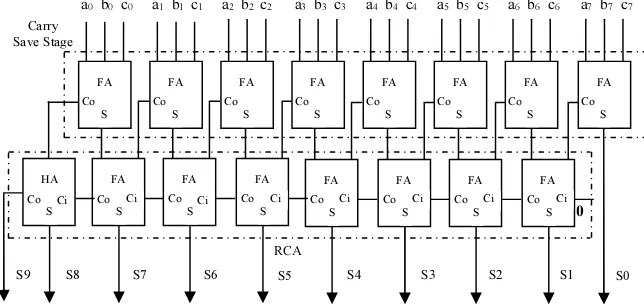
A carry save adder to add three inputs of eight bits each is shown in figure 5. It consists of a carry save stage and RCA/CLA stage. The carry save stage requires n full adders where n represents the number of bits in each input. The sum and the carry bits of all the n full adders of the carry save stage are independently and simultaneously calculated based on the current input bits in O(1) time. The final sum of n+1 bits is obtained by adding the sequence of sum bits with a left shifted carry sequence appended by a zero. Thus the time required to perform the addition of three input numbers is reduced to finding the sum of two numbers. This method of adding numbers can be extended indefinitely by adding an input at every level of carry save stage. There is no intermediate carry propagation however the final stage is a ripple carry adder or a carry look ahead adder. Hence the use of CSA tree results in higher speed when compared with that of Ripple carry adder tree and carry look ahead adder tree.
The conventional shift accumulator(SA) consists of a Accumulator,Right shift register and adder/subtractor units as shown in figure 1,2 and 3.The flowchart explaining the operation of a conventional shift accumulator(SA) is shown in figure 6.For the traditional shift accumulator method, the inputs from the input shifter section starts with the Least Significant Bit (LSB).The corresponding combinational sum of coefficients is given as the input to the SA section. This partial term is shifted right and added with the next partial result in every clock cycle. For the Most Significant Bit (MSB) combination input of the input shifter, the sign control signal S=1 and the corresponding partial term is subtracted from the accumulated value. The final output is obtained by taking out the
Figure 5: Carry Save Adder For Adding Three Inputs Of Eight Bits
Sign Control
Input
C6
C5
C4
C3
C0
C7
0
0
0
0
0
0
0
0 Input Shifter
Carry Save Adder Tree
+/- Accumulator
Shift Left
C1
C2
S (1 for MSB)
Y(n) b0
b1
b2
b3
b4
b5
b6
b7
S0 S1 S2
S3 S4
S5 S6
S7 S8 S9
Carry Save Stage
0 a2 b2 c2 a3 b3 c3 a4 b4 c4 a5 b5 c5 a6 b6 c6 a7 b7 c7
FA Co
S
FA Co
S FA
Co S
FA Co
S FA
Co S
FA Co
S FA
Co S HA Co
S FA Co
S
FA Co
S
FA Co
S
FA Co
S
FA Co
S
FA Co
S
FA Co
S FA
Co S a1 b1 c1
a0 b0 c0
RCA
[image:4.595.130.452.565.718.2]Least Significant bit of the accumulated value in every clock cycle which is costlier in terms of hardware usage and speed.
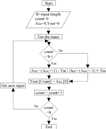
Figure 6: Flow chart for Conventional Shift Accumulator
[image:5.595.93.271.166.383.2]The flowchart explaining the operation of the modified shift accumulator(SA) is shown in figure 7.For the shift accumulator used in the proposed method, the input from the input shifter section begins with the Most Significant Bit (MSB).The corresponding combinational sum of coefficients which is the partial term from the CSA
Figure 7: Flow chart for Modified Shift Accumulator
tree is given as the input to the SA section. This partial term is shifted left and added with the next partial result in every clock cycle. For the first input of the input shifter which is the MSB bit of the samples, the corresponding first partial term is subtracted from the initialized accumulator. The final accumulated value after B clock cycles is the required output. Hence this modified shift accumulator(SA) results in saving the extra hardware that is required to take out the Least Significant bit of the accumulated value in every cycle for forming the output. If the partial result has lesser bits than the accumulated value, then each partial term has to be prefixed with ‘0’s for finding the correct sum of both the values.
4. IMPLEMENTATION AND RESULTS
The Shift Accumulator used in proposed method and Conventional Shift Accumulator were implemented using Xilinx Spartan 6slx150tfgg900-4 FPGA device and also on Xilinx Virtex 6vlx240tff1156-1FPGA device and a comparison of the performance metrics is presented in table 1 and table 2 .The results obtained clearly indicate that that the SA used in the proposed method requires less area usage (Number of slices) and also yields lesser delay and maximum usable frequency.
Table 1: Comparison of Performance Metrics of Shift Accumulator Unit Using Spartan 6 FPGA Device
[image:5.595.113.508.473.758.2](6slx150tfgg900-4)
Table 2: Comparison of Performance Metrics of Shift Accumulator Block Using Virtex 6vlx240tff1156-1
FPGA Device SA
Input in Bits
Used in the Proposed Method
Existing Method
No. of Slices
Delay (ns)
Maximum Frequency (MHz)
No. of Slices
Delay (ns)
Maximum Frequency (MHz)
8 3 2.50 400.11 9 2.93 341.05
16 6 2.74 365.19 17 3.10 322.47
20 7 3.25 307.83 24 3.89 256.93
32 10 3.52 284.04 37 4.16 240.22
SA Input
in Bits
Used in The Proposed Method
Existing Method
No. of Slices
Delay (ns)
Maximum Frequency (MHz)
No. of Slices
Delay (ns)
Maximum Frequency (MHz)
8 5 1.88 533.19 11 2.29 435.82
16 7 2.14 466.96 24 2.51 397.85
20 13 2.60 384.39 33 3.00 333
32 19 2.78 359.71 38 3.20 312.89
Get next input
Yes
Start
B=input length count=0 Acc=0,Yout=0
Get the input
Acc= (Acc>>1) - Yin
count = count+1
count =B
End Yout [Count] = Acc [0]
Acc= (Acc>>1) + Yin
No
Yes
count = B-1
No
Get next input
Start
B=input length count=0 Acc=0,Yout=0
Get the input
Acc= (Acc<<1) - Yin
count = count+1
End
Acc= (Acc<<1) + Yin
No
Yes
count = 0
Yout=Acc
Yes
count =B
[image:5.595.102.286.493.718.2]Table 1 and table 2 also clearly indicate that a same design when implemented using Spartan series results in lesser number of slices compared to Virtex series. Another inference from table1 and table2 is that the Maximum frequency of operation of a design is very high when implemented using Virtex series than the Spartan series.
To prove the performance enhancements of proposed architecture, LUT-less DA based FIR filters using Multiplexers and RCA tree [11], LUT-less DA FIR filters using tri-state buffers and CLA tree [12], and the proposed architecture were implemented using Xilinx Spartan 6slx150tfgg900-4 FPGA device and also on Xilinx Virtex 6vlx240tff1156-1 FPGA device for an input bit width of B=20 and 8 bit coefficients for filter orders varying from 8 to 64.Table 3 and Table 4 clearly shows that for all values of N ranging from 8 to 64,the proposed architecture is superior to the existing methods of DA Based LUT-Less FIR filter in terms of number of occupied slices and maximum frequency. This is very well justified for the carry save adder requires less computation time resulting in maximum frequency when compared with the ripple carry adder and carry look ahead
adder. Additionally the modified shift accumulator results in very less area usage and high frequency. Figure 8 also shows that the proposed architecture requires lesser number of Slice LUTs when compared with existing methods.
Figure 8: Comparison of No of Slice LUTs of the Proposed and Existing Methods of DA Based
LUT-Less FIR Filters Using Spartan 6 FPGA device.
Table 3: Comparison of Performance Metrics of the Proposed and Existing Methods of DA Based LUT-Less FIR Filters Using Spartan 6 Family. (6slx150tfgg900-4)
Order of Filter
Proposed Method Yoo And Anderson[11] Eshtawie [12]
No. of occupied
Slices
Minimum period
(ns)
Maximum Frequency (MHz)
No. of occupied
Slices
Minimum period
(ns)
Maximum Frequency (MHz)
No. of occupied
Slices
Minimum period
(ns)
Maximum Frequency (MHz)
8 Tap 73 13.85 72.18 115 15.41 64.89 105 15.14 66.05
16 Tap 127 16.74 59.75 168 18.46 54.18 165 18.26 54.76
32 Tap 278 20.56 48.63 320 22.04 45.38 416 21.71 46.06
64 Tap 547 23.10 43.29 642 24.14 41.43 867 24.81 42.03
Table 4: Comparison of Performance Metrics of the Proposed and Existing Methods of DA Based LUT-Less FIR Filters Using Virtex 6 Family. (6vlx240tff1156-1)
Order of Filter
Proposed Method Yoo And Anderson[11] Eshtawie [12]
No. of occupied
Slices
Minimum period
(ns)
Maximum Frequency (MHz)
No. of occupied
Slices
Minimum period
(ns)
Maximum Frequency (MHz)
No. of occupied
Slices
Minimum period
(ns)
Maximum Frequency (MHz)
8 Tap 89 10.32 96.90 109 11.46 87.29 140 11.37 87.96
16 Tap 195 12.51 79.93 215 13.37 74.79 217 13.3 75.19
32 Tap 346 15.24 65.63 393 15.91 62.87 516 15.71 63.67
5. CONCLUSION
In this paper, a new DA based LUT less FIR filter using carry save adder tree and a modified shift accumulator is presented .The implementation results of the proposed architecture showed significant reduction in delay and area over the existing methods of DA Based LUT-Less FIR Filters. The reduction in computation time is achieved by using the carry save adder. Further reduction in delay and area was achieved due to the modified shift accumulator. The implementation results of 8-tap filter for an input bit width of B=20 and 8 bit coefficients using Spartan FPGA device shows 36.52% savings in area and 10.12% reduction in delay when compared with LUT less DA using RCA and 30.47%savings in area 8.52% reduction in delay when compared with LUT less DA using CLA. Future work is to develop more algorithms and architectures for area-delay-power-efficient implementation of FIR filters and adaptive FIR filters based on DA to meet the growing requirements of DSP applications.
REFRENCES:
[1] J. G. Proakis and D. G. Manolakis, Digital Signal Processing: Principles, Algorithms and Applications., NJ: Prentice-Hall, 1996.
[2] K. K. Parhi, VLSI Digital Signal Processing Systems: Design and Implementation. New York: Wiley, 1999.
[3] G. R. Goslin, “A Guide to Using Field Programmable Gate Arrays (FPGAs) for Application-Specific Digital Signal Processing Performance”, XILINX, 1995.
[4] M. Yamada, and A. Nishihara, “High-Speed FIR Digital Filter with CSD Coefficients Implemented on FPGA”, Proc. IEEE Design Automation Conference, 2001, pp. 7-8.
[5] M. D. Macleod and A. G. Dempster, “Multiplierless FIR filter design algorithms”,
IEEE Signal Processing Letters, vol. 12, no. 3, pp. 186–189,Mar. 2005.
[6] A. Croisier, D. J. Esteban, M. E. Levilion, and V. Rizo, “Digital filter for PCM encoded signals”, U.S. Patent 3 777 130, Dec. 4, 1973. [7] A. Peled and B. Liu, “A new hardware
realization of digital filters”,IEEE Transactions on Acoustic, Speech, Signal Processing, vol. 22, no. 6, Dec. 1974, pp.456–462.
[8] S. A. White, “Applications of the distributed
arithmetic to digital signal processing: A tutorial review”, IEEE ASSP Mag., vol. 6, no. 3, July, 1989, pp. 5–19.
[9] K.G.Shanthi and N.Nagarajan,”Memory based hardware efficient implementation of FIR Filters”, International review on computer
and software (IRECOS), July 2013vol.8, no.7,
pp.1718-1726.
[10] P. Choi, S.-C. Shin, and J.-G. Chung, “Efficient ROM size reduction for distributed arithmetic”, Proceedings of the IEEE International. Symposium. Circuits System (ISCAS), May 2000, vol. 2, pp. 61–64. [11] H. Yoo and D. V. Anderson,
“Hardware-efficient distributed arithmetic architecture for high-order digital filters”, Proc. IEEE Int. Conf. on Acoustics, Speech, Signal Processing (ICASSP), Mar. 2005, vol. 5, pp. v/125–v/128. [12] Mohamed A. Eshtawie and Masuri Othman, “On-Line DA-LUT Architecture for High-Speed High-Order Digital FIR Filters”,
IEEE international conference on
communication systems, Singapore, Nov 2006.
[13] Patrick Longa and Ali Miri, “Area-Efficient FIR Filter Design on FPGAs using Distributed Arithmetic”, IEEE International Symposium on Signal Processing and Information Technology, 2006, pp.249-252.
[14] S.-S. Jeng, H.-C. Lin, and S.-M. Chang, “FPGA implementation of FIR filter using M-bit parallel distributed arithmetic,”
Proc.2006,IEEE Int. Symp. Circuits Systems (ISCAS), May 2006, p. 4.
[15] P. K. Meher, S. Chandrasekaran, and A. Amira, “FPGA realization of FIR filters by efficient and flexible systolization using distributed arithmetic,”IEEE Transactions on Signal Processing., vol. 56, no. 7, July 2008, pp. 3009–3017.
[16] Jiafeng Xie n, Jianjun He, Guanzheng Tan,” FPGA realization of FIR filters for high-speed and medium-speed by using modified distributed arithmetic architectures”,
Microelectronics Journal 41, April 2010 pp. 365–370.
[17] R.Uma, VidyaVijayan, M.Mohanapriya and Sharon Paul, “Area, Delay and Power
Comparison of Adder Topologies”,
International Journal of VLSI design &
Communication Systems (VLSICS), Vol.3,