http://dx.doi.org/10.4236/cs.2016.78114
A New Fully Differential Adaptive CMOS Line
Driver Using Fuzzy Controller Suitable for
ADSL Modems
Ali Dadashi, Yngvar Berg, Omid Mirmotahari
Department of Informatics, University of Oslo, Oslo, Norway
Received 12 February 2016; accepted 10 March 2016; published 8 June 2016
Copyright © 2016 by authors and Scientific Research Publishing Inc.
This work is licensed under the Creative Commons Attribution International License (CC BY).
http://creativecommons.org/licenses/by/4.0/
Abstract
In this paper, a new principle for an adaptive line driver using Fuzzy logic is presented. This type of line driver can adapt its output impedance and gain, automatically to the applied load using a fuzzy logic controller (FLC). This results in automatically corrected output impedance for different cables with terminations. Also, the line driver output impedance and gain become insensitive to process and line variations. As an example, a line driver for ADSL application has been designed. The circuit operates from a 3.3 v in a 0.35 um standard CMOS technology. The power consumption of FLC is about 1 mW. The circuit dissipates 106 mW and exhibits a −62 dB THD for a 3.2-Vpp sig-nal at 5 MHz across a 75 ohms Load. It has a relatively high −3 dB bandwidth (240 MHz) with good phase margin of about 67 degrees in a 10 pF load capacitor.
Keywords
Fuzzy Logic Controller (FLC), ADSL Modem, Adaptive Line Driver, Folded Cascode Power Supply Noise, Class A/B
1. Introduction
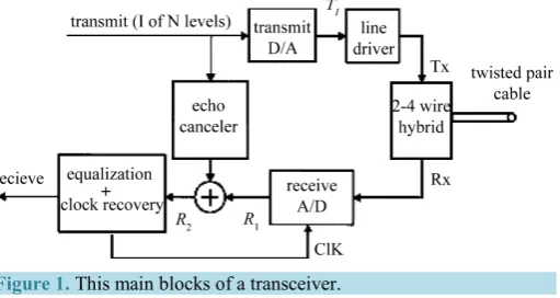
Figure 1. This main blocks of a transceiver.
important. But a great trend exists in designing CMOS line drivers to achieve a full CMOS AFE (analog front end) on a chip. Line drivers (LD) are op-amps, but with higher current-driving capability of very low resistive loads. In LDs, output stage is the most important component compared to the other parts of the LD. In most LDs, class-AB output stages preferred to the other output stage classes. The load which is nominally between 50 and 100 varies upon the cable length, temperature and other external effects, and this causes the reflections in the line. To minimize reflections, the source and load impedances of the transmission line have to be equal to the characteristic impedance of the line. In traditional architectures, there is a 6-dB signal loss incurred in the exter-nal resistors that implement cable termination which adds to the inefficiency of the driver [1]. An approach that provides integrated termination with no signal loss in the termination is also a desirable feature for LDs. In this paper, a novel method for an adaptive LD based on Fuzzy logic controller (FLC) with no signal loss in termina-tion is introduced. An adaptive tuning scheme for output impedance matching using peak detectermina-tion is used to provide uniform performance across line impedance variations. The use of fuzzy systems is widespread, mainly in the control field. Furthermore, in many applications the knowledge describing the expected behavior of the system is contained on data clusters. Due to this, the designer has to elaborate the IF-THEN rules according to such data; if the data clusters are too large, it could imply a tremendous effort. Neural networks can learn from data clusters, so it results natural thinking in a methodology which gathers the characteristics of both systems, combining explicit knowledge representation of fuzzy logic with the learning capability of neural networks. In this way, the called neuro-fuzzy systems are obtained. Among the various inference methods reported in the li-terature, the singleton or zero-order Takagi-Sugeno-Kang’s (TSK) method is very adequate for hardware im-plementations. Functionally, the ANFIS architecture is equivalent to a TSK zero order and/or first order fuzzy system [2]. In [3], ANFIS architecture is discussed and optimized using a new algorithm. This algorithm is suited to use in CMOS circuits. In this paper, a two input, one output current mode FLC based on [4] is de-signed. In this structure the output impedance and gain of the LD can be controlled by using a Fuzzy controller.
This paper is organized as follows: in Section 2 the blocks of the LD are explained and the circuit specifica-tions, such as the differential gain and frequency response are calculated. Also a circuit to compensate tempera-ture, process variations and supply noise is proposed in this Section. In Section 3, the FLC used in this structure is explained. Simulation results are reported in Section 4. Finally, Section 5 concludes the paper.
2. LD Design
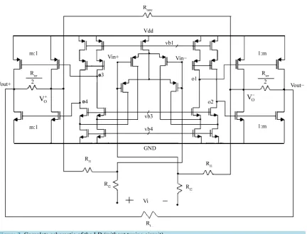
Figure 2 shows the simplified schematic of the closed loop part of the LD (without tuning circuit). By assuming that the amplifier’s gain is high, the overall gain depends on resistance feedback network and it is obviously equal to:
1
2
diff f
diff f
Vo R
Vi = −R (1)
Figure 2. Simplified schematic of the closed loop part of the LD, that is not tunable.
Figure 3. Complete schematic of the LD (without tuning circuit).
0 1 2
f
v v v
A =A ×A
(2)
and Av1, Av2 are the dc-gain of the first stage and output stage, respectively. The Polysilicon resistance is used to implement circuit resistors because it is more linear than others (p-well or n-well resistances). Because of us-ing fully differential architecture, common-mode disturbances, such as substrate or power supply noise are can-celled to a great extent. In addition, even order harmonics are also eliminated. In this work, two separate mon-mode feedback circuits are used in the two stages due to fast transient, instead of using an overall com-mon-mode feedback which is usually slow. This helps to achieve a much reduced distortion [5].
2.1. First Stage of the LD
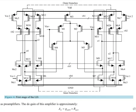
Figure 4. First stage of the LD.
as preamplifiers. The dc-gain of this amplifier is approximately:
1 1 1
v mM out
A =g ×R (3)
[
]
(
)
[
]
out1≈ mM10× oM10× oM12 mM8× oM8× oM6 oM1 mMc6× oMc6× oMc5
R g r r g r r r g r r (4)
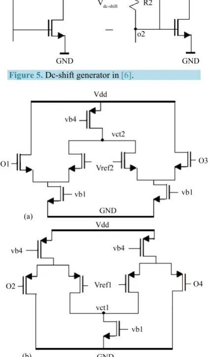
Figure 5. Dc-shift generator in [6].
Figure 6. Common-mode feedback circuit of the first stage (a) Common-mode feedback circuit for branch with higher common-mode voltage level. (b) Common-mode feedback circuit for branch with lower common-mode voltage level.
code nodes in the conventional circuits (e.g. [6]). So the capacitance of cascode nodes is reduced and they will be faster nodes.
2.2. Second Stage of the LD
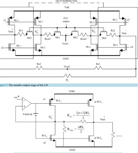
Figure 7 shows the complete schematic of the output stage of the LD without common-mode feedback circuits. As mentioned before, the second stage of the LD is a widely used class A/B power amplifier output stage, which delivers load current with some voltage gain.
[image:5.595.208.420.181.543.2]de-vices are in the triode region, and form the tunable resistors. The gate voltage of these dede-vices will be tuned with a FLC to correct the output impedance and gain of the LD. Impedance matching is done using a topology wherein, when the output voltage(Vout) is equal to the input, the output resistance is matched to the line [1] [8]. This scheme has the advantage that it can adjust to external line as well as internal process variations. The dc-gain of the output stage can be calculated as:
(
)
2 = 6+ 8 × tune
v mMo mMo
A g g R
(5)
From Figure 7 and Figure 8 the output impedance of the LD is achievable. To calculate the output imped-ance of the LD, test voltage (Vx) is applied to the output node (Vout) and the current produced is calculated. With writing a KCL in the output node (Equation (6)), and calculating Ix (current of Vx), the output impedance
[image:6.595.96.538.220.710.2]Figure 7. The tunable output stage of the LD.
is equal to Equation (7). (Notice that to calculate the output impedance, the Vo node is virtual ground because of the external resistive feedback network effect).
(
)
out 1 ⋅ + = ⇒ = = + ter ter ter RVx m Vx Ix R Vx
R R Ix m
(6)
(
)
(
(
)
3 4)
1 2
out 1 1
+ + +
= =
+ +
r r
z z M M
ter R R R R
R R
m m (7)
(
1 2 r3 r4)
(
1)
ter z z M M L
R = R +R +R +R = n+ ⋅R (8) Parameter m, is the size ratio of devices Mo1,4 to Mo5,6 and devices Mo2,3 to Mo7,8. Indeed this parame-ter (m) is the current mirroring ratio of the output stage devices. There is a trade off in the designing the para-meter m. Larger m causes the larger parasitic capacitor in the output nodes of the first stage (o1, o2, 03, o4), and reduces the speed of the feedback loop and linearity in the higher frequencies. In the opposite side, larger m re-duces the power consumption of the first stage by reducing the bias currents of the feedback loop devices. Con-sidering this trade off, the optimum size can be found which gives good open-loop and closed-loop linearity and reasonable power consumption, by trial and error approach and considering the simulation results. According to this method, m is designed to be 30. The sizes of output stage devices are shown in Table 1. To calculate the voltage gain from Vo+ to Vout+ in Figure 8 we can write:
out tune
⋅ ⋅ L =
Vo m R V
R
(9)
(
)
tune= cm1+ cm2+ Mr1+ Mr2 = ⋅ L
R R R R R n R (10)
(
1 2)
out
tune 1 2
⋅ ⋅
= = =
+ + r + r
L L
v
o cm cm M M
V m R m R
A
V R R R R R (11)
and
(
)
1, 4
1, 4
1, 4 1, 4 1, 4
r r
Mr Mr M
ox Mr Mr Mr Mr Mr Mr
L R
C Wµ Vgs Vt
=
− (12)
and VgsMr Mr1, 4 =
(
VoFLC−Vcm1,2)
where VoFLC is the output voltage of the FLC. And Vcm1,2 is the common-mode voltage of the output nodes
which is equal to 1.65 volt. From Equations ((7)-(9), (11))
L v
L
m R m
A
n R n
⋅
= =
⋅ (13)
(
)
(
)
out 1 1 + = + L n R Rm (14)
And if the parameters n and m become equal (n = m), then: Av = 1 and Rout =RL . This condition happens by
[image:7.595.89.540.661.722.2]tuning Mr1-Mr4 devices with a FLC. In this case the termination (impedance matching) is done and reflections are eliminated. But if the impedance of the cable varies, the reflections appear in the line again and the perfor-mance of the driver will be degraded. The nominal value of RL is 75 Ω. To minimize reflections, the output im-pedance of the driver must be controlled and this can be performed by tuning of Rter and Rtune with a FLC. It
Table 1. Size of transistors used in the output stage.
Transistor Wµm/Lµm Transistor Wµm/Lµm
MO1 1200/0.35 MO5 40/0.35
MO2 3600/0.35 MO6 40/0.35
MO3 3600/0.35 MO7 120/0.35
is clear that in this structure load variation directly changes the peak voltage of the output node (Vout+ ). Hence for detecting load variations, the peak voltages of the input and output (Vout+ ) nodes of the LD should be compared. Indeed the peak voltage of Vo+ is compared with peak voltage of Vout+ . It is clear that the common-mode vol-tage of the input volvol-tage is not a constant value, so Vi+ and Vout+ do not have the same common-mode voltages and comparison of the positive peak voltages of these nodes is not reasonable. First input of the FLC is the dif-ference of positive peak voltages of Vo+ and Vout+ nodes (e).
out+ − +− = P P− oP P
e V V
(15) Another input of FLC, is the variation of the e (∆e). The voltage peak detector circuit is shown in Figure 11. Devices Mr1- Mr2 and Rcm1-Rcm2 have another role. They have been used in the output stage common-mode feedback loop. They provide the average voltage of the output nodes. Tuning these devices has a negligible ef-fect on the performance of the output stage common-mode feedback circuit.
2.3. Frequency Response
The proposed LD has many poles and zeros, but two first poles or zeros are important in the frequency response ofthe op-amp. Figure 9 is used for calculating frequency response of the LD. From Figure 9, the transfer func-tion of closed loop part of the LD (Av1) is:
( )
( )
01 in 1 2 1 1 = = + + vf o v A V
A s s
V S S
P P
(16)
and Avf0 is dc-gain of the LD and is equal to:
0 1 2
f
v v v
A =A ×A
(17) By using miller effect [7] P1, the pole which occurs in the output node of first stage is :
1 out1 1 1 = − × o P
R C (18)
1 1 2 2 2 7
o v gdMo v gdMo
C ≈C A C+ ⋅ +A C⋅
(19)
1 dMc6 dM8 dM10
C =C +C +C (20)
[
]
(
)
[
]
out1≈ mM10× oM10× oM12 mM8× oM8× oM6 oM1 mMc6× oM6× oM5
R g r r g r r r g r r (21)
and by using miller effect [7], P2, the pole which occurs in the output node (V0+) is:
2
1 7 7 1
2 2
7 7 7 1
1
gdMo gdMo
gdMo mMo gdMo
P
c c c c
R c
c g c c
[image:8.595.99.537.304.710.2]≈ − + ⋅ × + ⋅ +
(22)
tune
2 = 2 5 7 oMO oMO
R
R r r (23)
2 dM5 dM7
C =C +C
(24) Also from Figure 9, the total transfer function of the LD is:
( )
out( )
0 in 1 2 1 1 = = + + vf v A VA s s
V S S
P P
(24)
where P1 is equal to Equation (18) and by using miller effect, P2 is:
2
1 2 2 1
out out
2 2 2 1
1 ≈ − + ⋅ × + ⋅ + gdMo gdMo
gdMo mMo gdMo
P
c c c c
R c
c g c c
(25)
out 6 8
2 = + + L dMo dMo C
C C C (26)
out = 2 1 2
L
oM O oMO R
R r r (27)
In [6], load capacitor (CL) is directly connected to the output node of the LD, and reduces the second pole of
the LD which is occurred in the output node. Therefore the phase margin of the LD is also reduced by the load capacitor and also compensating of the LD, causes a reduction in the UGB and speed of the LD. But in the pro-posed structure opposite to [6], the load capacitor is out of the feedback loop and is not connected directly to the output node (Vo) of the feedback loop and does not reduce the phase margin of the LD. Therefore a fast
feed-back loop and so higher linearity in the higher frequencies can be achieved, in the same power consumption. It is considerable that the calculated frequency response in this section is correct only for a fixed load (impedance of the cable). It should be noted that a change in the load of the driver will result in a change in the frequency re-sponse of the driver.
2.4. Temperature and Process Variations and Power Supply Noise
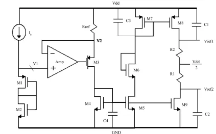
Circuit for generating Vref1 and Vref2 (reference voltages of the first stage’s common-mode feedback circuits) is shown in Figure 10. This circuit can compensate the process and temperature variation effects for output stage devices as well as the bias circuit in [6], but in this work, unlike in [6], there is not any resistor in the dif-ferential signal path (Figure 10). In the case of temperature variations the most sensitive parts of the LD are the large output stage devices. As the temperature increases the threshold voltage of these devices decreases. This variation causes to increase the bias current of the output stage devices and forces extra power consumption to the circuit. Furthermore temperature variations, force an extra distortion to the circuit. To reduce the effect of temperature variation in the bias current of the output devices, a technique is used in the circuit shown in Figure 10. As mentioned before the temperature increase, increases the bias current of the output stage devices, so the main idea is to prevent the bias current increase in these devices. By decreasing the gate-source voltages of these devices with temperature increase, the overdrive voltage of these devices will remain fixed to a great extent. As temperature increases, the bias current of M1 and M2 devices increase in the circuit of Figure 10 as well as the current of output devices. Hence the voltage of V1 decreases in order to keep the current of M1 and M2 transis-tors constant. By decreasing the voltage of V1, the voltage of V2 decreases, too and so the current of reference resistor (Rref ) increases. This bias current increase happens in the M3-M9 devices and causes increase of the
Figure 10. Reference voltages (Vref1, Vref2) generator circuit for input stage common-mode feedback circuit.
fixed to a great extent and temperature increase cannot change the bias current of output devices.
The same concept occurs when the temperature decreases. Temperature reduction decreases the bias current of output devices. And the same decrease occurs in the bias current of M1 and M2 devices. So the voltage dc-shift between the gates of output stage devices decreases using circuit of Figure 10. Hence the bias currents in these devices remain constant. As mentioned before this circuit (circuit of Figure 10) minimizes the effect of temperature variation on the performance of LD by providing a negative feedback process to adjust the bias current of the output stage devices. Although the temperature variations can change the threshold voltage of the other transistors in the circuit (e.g. first stage’s devices and M3-M9 in the circuit of Figure 10), most of them are current mirror devices and so the temperature variations cannot influence the bias currents of them signifi-cantly.
This circuit can compensate the power supply noise effect on the LD. Although the designed LD is a fully differential circuit and can eliminates common-mode type noises such as power supply noise, any mismatch between the devices of two parts of the differential output stage of LD causes to remain a portion of the power supply noise in the output voltage of the LD. This degrades the THD and the performance of the LD. So reduc-ing the effect of power supply noise on the each sides of the LD improves the performance of the LD. Power supply noise directly changes the Vgs of the output devices because the source of these devices is connected to Vdd and GND. To compensate this effect the gate voltage of these devices must be changed with supply noise in order to keep the Vgs of the output stage devices constant. To change the gate voltages of these devices, some capacitors (c1-c4) are added to the circuit of Figure 10. These capacitors apply the power supply noise to the Vref1 and Vref2 nodes. Also the common mode feedback circuits of the first stage transfers the power supply noise from Vref1 and Vref2 to the gates of the output stage devices. Therefore the power supply noise cannot change the Vgs of the output stage devices to a great extent. So the significant portion of the noise caused by the power supply noise in the output voltages of the LD is reduced by using this technique and the PSRR of the LD improves.
circuit a reference current which is sensitive to the resistance variation is produced and mirrored to the M8 and M9 devices and passes from R1 and R2 resistors. The reference current is:
(
dd 2)
ref
ref
V V
I
R
−
= (28)
The process variation cause an approximately equal change in the value of resistors (R R R1, ,2 ref) in the circuit
of Figure 10, so the dc shift (Vref1-Vref2) remains constant to a great extent. The op-amp used in the circuit of Figure 10 is a simple single stage amplifier with very low bias currents to minimize the power consumption.
3. Controller Design
Figure 11 shows the simplified block diagram of the designed adaptive LD. As mentioned before in the pro-posed LD impedance matching is done using a topology wherein, when the output voltage is equal to the input, the output resistance is matched to the line [1] [8]. The interface block shown in Figure 11, consists of peak de-tector and differentiator circuits. The peak dede-tector circuits are used to extract the peak voltages of the output nodes (Vo+, Vout+ ). The voltage peak detector circuit is shown in Figure 12. In this circuit the capacitors charge with larger currents, proportional to the voltage of Vo+ and Vout+ , but discharges with lower currents which are the bias currents of the Mp3 and Mp4 devices (Notice that the capacitors discharge when the voltage of the out-put nodes goes down). Therefore these circuits can detect the peak voltages of the outout-put nodes (Vo+, Vout+ ) with a voltage dc-shift. This dc-shift has a negligible effect on the performance of the controller, because the differ-ence of peak voltages is important in the impedance matching process. First input of the FLC is the differdiffer-ence of positive peak voltages of Vo+ and Vout+ (e). Another input of FLC, is the variation of the e (∆e). The differen-tiator circuit has a simple structure that is not discussed in this paper.
The complete block diagram of the used neuro-fuzzy controller is shown inFigure 13. This FLC is based on ANFIS architecture [3] that can easily provide a mapping between stipulated input/output data pairs. The pro-posed controller is investigated in detail in [4]. By applying some changes to [4], it has been used to control the output impedance and the gain of the LD. The modified controller has 2 inputs, 9 rules, and 9 singletons. Each input has bell-shape membership functions with 4 bit digital input, to control its slope. The characteristics of the membership functions (slope and position) can be tuned by using learning algorithm [4] to reduce the total error
[image:11.595.203.426.442.721.2]Figure 11. System block diagram of the adaptive LD.
Figure 13. Block diagram of the neuro-fuzzy controller.
Table 2. Employed rule base.
e
Δe N Z P
N P P Z
Z P Z N
P Z N N
of the mapping. All blocks of the FLC (except the fuzzifier block) are in current mode, so the controller is sim-ple. Each block has high accuracy, low power consumption, and small occupied area [4]. By using modified ANFIS architecture, in the defuzzifier block the divider circuit has removed [4], therefore the occupied area and power consumption of FLC has reduced. Transistor level circuit of each layer is described in [4].
Inference Engine and Rules
Each input e and ∆e has three membership functions labeled Negative (N), Zero (Z), and Positive (P) that pro-vide 9 rules. From Table 2:
Rule1: If e is N and ∆e is N then out is P. Rule2: If e is N and ∆e is Z then out is P. Rule3: If e is Nand ∆e is P then out is P. ...
Rule9: If e is Pand ∆e is P then out is N.
4. Simulation Results
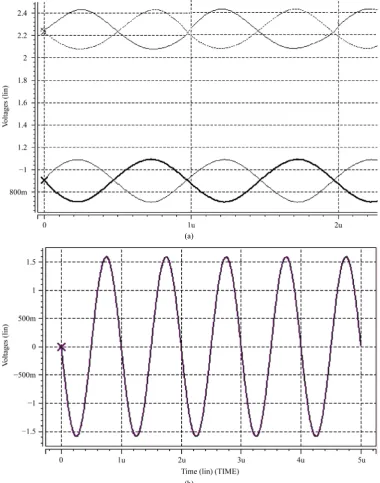
In this section, the simulation results of the proposed LD are shown and the proposed LD is compared with the some conventional LDs. The proposed LD has been designed in a typical 0.35 μm CMOS process and is simu-lated by HSPICE software using level 49 parameters (BSIM3v3). Transient response and Ac response of the LD are shown for a constant load (RL = 75 Ω, CL = 10 pF) in Figure 14 and Figure 15. Figure 14(b) shows a 3.2
p p
V − output waveform of the LD. The LD drives a 75 ohms resistive load and 10 pF single-ended capacitors
the power supply noise in the THD of LD is reduced to a great extent by using this circuit. Table 3 summarizes the THD of the LD in the different RL and different frequencies in 3.2 Vp-p output voltage swings. Table 4 summarizes the THD of the LD in the different output voltage swings. Table 5 summarizes the main features of this design and compares it with some recent works. It shows that bandwidth, power consumption and especially THD performance, are considerably improved compared to the other designs. To show the performance of the FLC, error (e) and change of error (Δe) signals are applied to the FLC. Also a differential 90 Ω load is connected to the output nodes of the LD. As shown in Figure 18 termination (e ≈ 0) has been done by FLC in about 28 usec. After 110 usec the load resistor (RL) is changed to 75 Ω. In this case the impedance termination has been done in about 15 usec. The simulation result of the impedance termination is shown in Figure 19.
(a)
[image:13.595.123.504.205.689.2](b)
Figure 15. Closed-loop frequency response of the output of the LD driving a 75 Ω and 10 pF load (Magnitude).
Figure 16.Open-loop magnitude and phase of the LD output while driving a 75 Ω and 10 pF load.
5. Conclusion
[image:14.595.116.512.321.624.2]Figure 17. A 3.2 VP-P output spectrum of the LD while driving a 75 Ω and CL = 10 pF load at 1 MHz.
(a)
(b)
[image:15.595.107.523.215.678.2]Table 3. THD in different RL and different frequencies. 1 MHz 800 KHz 500 KHZ 300 KHz 100 KHz Fin 63 dB 70 dB 72 dB 77 dB 80 dB RL= 60
67 dB 73 dB
76 dB 80 dB
84 dB RL = 75
70 dB 75 dB
78 dB 82 dB
86 dB RL = 90
Table 4. THD in different output voltage swings (Rl = 75, Fin = 1 Mhz).
2.5 2.7
3 3.2
Output swing (v)
86 dB 77 dB
72 dB 67 dB
THD
Table 5. Circuit characteristic and comparison.
Parameters This work [6] [1] [8]
Power supply 3.3V 3.3V 3.3V 3.3V
Technology (µm) 0.35 0.35 0.35 0.5
Power dissipation (mW) 107 140 155 -
Load range 60 - 90 Ω - 60 - 90 Ω 70 – 180 Ω
−3dB Freq (MHz) 240 261 160 15
THD (dB) −62 3.2 Vpp 5 MHz −74.5 3.3 Vpp 10 MHz −47.5 2 Vpp 10 MHz −45 1.2 Vpp 5 MHz
Maximum output voltage swing (v) 3.8 3.8 2 1.6
Adaptive yes no yes yes
[image:16.595.88.541.201.618.2]
Figure 19. Simulation result of the structure for cable impedance variations (90 to 75 ohm). (a) Output of FLC (b) Error voltage (e).
References
[1] Mahadevan, R. and Johns, D.A. (2000) A Differential 160-MHz Self-Terminating Adaptive CMOS Line Driver. IEEE Journal of Solid-State Circuits, 5, 1889-1894. http://dx.doi.org/10.1109/4.890302
[2] Jang, J. (1993) ANFIS: Adaptive-Network-Based Fuzzy Inference System. IEEE Transactions on Systems, Man, and Cybernetics, 23, 665-685. http://dx.doi.org/10.1109/21.256541
[3] Peymanfar, A., Khoei, A. and Hadidi, Kh. (2007) A New ANFIS Based Learning Algorithm for CMOS Neuro-Fuzzy Controllers. The 14thIEEE International Conference on Electronics, Circuits and Systems, Marrakech, 11-14 Decem-ber 2007, 890-893. http://dx.doi.org/10.1109/icecs.2007.4511134
[4] Peymanfar, A., Khoei, A. and Hadidi, Kh. (2009) Design of a General Propose Neuro-Fuzzy Controller by Using Modified Adaptive-Network-Based Fuzzy Inference System. International Journal of Electronics and Communica-tions, 60, 557-566.
[5] Hadidi, Kh., Oshima, H., Sasaki, M. and Matsumoto, T. (2002) A Highly Linear Fully Differential Low Power CMOS Line Driver. Proceeding of Europe Solid-State Circuits Conference, Portugal.
[6] Oskooei, M.S., Hadidi, K. and Khoei, A. (2005) A Highly Linear and Large Bandwidth Fully Differential CMOS Line Driver Suitable for High-Speed Data Transmission Applications. IEICE Transactions on Fundamentals of Electronics and Computer Sciences, E88-A, 416-423. http://dx.doi.org/10.1093/ietfec/E88-A.2.416
[7] Razavi, B. (2001) Design of Analog CMOS Integrated Circuits. McGraw-Hill, Boston.