Physical Characterization of Arbiter PUFs
Shahin Tajik1, Enrico Dietz2, Sven Frohmann2, Jean-Pierre Seifert1, Dmitry Nedospasov1, Clemens Helfmeier3, Christian Boit3, Helmar Dittrich2
1
Security in Telecommunications, Technische Universit¨at Berlin, Germany {shahin,jpseifert,dmitry}@sec.t-labs.tu-berlin.de
2Teraherz Spectroscopy, Technische Universit¨at Berlin, Germany {dietz,sf}@physik.tu-berlin.de
3Semiconductor Devices, Technische Universit¨at Berlin, Germany {clemens.helfmeier,christian.boit}@tu-berlin.de
Abstract. As intended by its name, Physically Unclonable Functions (PUFs) are considered as an ultimate solution to deal with insecure stor-age, hardware counterfeiting, and many other security problems. How-ever, many different successful attacks have already revealed vulnera-bilities of certain digital intrinsic PUFs. Although settling-state-based PUFs, such as SRAM PUFs, can be physically cloned by semi-invasive and fully-invasive attacks, successful attacks on timing-based PUFs were so far limited to modeling attacks. Such modeling requires a large sub-set of challenge-response-pairs (CRP) to successfully model the targeted PUF. In order to provide a final security answer, this paper proves that all arbiter-based (i.e. controlled and XOR-enhanced) PUFs can be com-pletely and linearly characterized by means of photonic emission analy-sis. Our experimental setup is capable of measuringeveryPUF-internal delay with a resolution of 6 picoseconds. Due to this resolution we in-deed require only the theoretical minimum number of linear independent equations (i.e. physical measurements) to directly solve the underlying inhomogeneous linear system. Moreover, we neither require to know the actual PUF challenges nor the corresponding PUF responses for our physical delay extraction. On top of that devastating result, we are also able to further simplify our setup for easier physical measurement han-dling. We present our practical results for a real arbiter PUF implemen-tation on a Complex Programmable Logic Device (CPLD) from Altera manufactured in a 180 nanometer process.
Keywords: Arbiter PUF, photonic emission analysis, backside, physical characteriza-tion
1
Introduction
characteristics, they can generally be categorized in two distinct classes of PUFs: settling-state-based PUFs and timing-based PUFs [15]. The former is based on bistable circuits such as SRAMs, while the latter is based on intrinsic differences in timing of a set of symmetric circuit paths.
Althoughunclonabilityandunpredictabilityare the main PUF requirements [3, 22], previous work in the literature has shown how different PUFs can be attacked and cloned. Settling-state-based PUFs such as SRAM PUFs can be characterized and cloned physically by semi-invasive and fully invasive attacks [10, 20]. Timing-based PUFs such as Arbiter PUFs are vulnerable to machine-learning attacks, which make it possible to emulate the PUF response [12, 24]. However, machine-learning attacks require a large number of challenge-response pairs (CRP) to pre-dict the response with high probability. Any non-linearity in the PUF response can negatively impact the effectiveness of machine-learning techniques [13, 32]. As a result substantially more CRPs together with extra side channel informa-tion are required to model the PUF response successfully [16]. However, in a real attack scenario, the intrinsic PUF response may be unavailable to the at-tacker [8, 14]. Moreover, trying a large set of CRPs may also be infeasible due to other countermeasures implemented on modern secure devices [23].
This work demonstrates that arbiter PUFs and more generally, timing-based PUFs can be characterized by high-resolution temporal photonic emission anal-ysis from the chip’s backside. This approach does not need any readout of PUF response nor does it require a substantial number of challenges to characterize the PUF. Our methodology is based on measuring the time difference between enabling the PUF and photon emission at the output of the last stage. For our Proof-of-concept (PoC), we have implemented an arbiter PUF on a Complex Programmable Logic Device (CPLD). The delay between the input of the PUF and the output of photodetector can be measured with an overall resolution of approximately 6 picoseconds by a Time-to-Digital Converter (TDC). As a result, the PUF response is determined by comparing the measured delays on both PUF chains. Furthermore, in our methodology, the required challenges for the physical characterization of the PUF increase linearly with PUF length. Finally, based on a mathematical approach we find the minimum number of necessary challenge combinations, which are required to characterize the PUF. Using this method-ology it also possible to characterize controlled PUFs [8], where the challenge is inaccessible to the attacker. As compared to other characterization techniques, such as machine learning, this methodology greatly reduces the amount of mea-surements that are necessary to characterize the intrinsic PUF behavior. The main contributions of this paper are as follows:
measurements than individual PUF stages, our methodology requires just two measurements per PUF stage.
Low-cost measurement setup for measuring the delay with the res-olution of 6 ps.We introduce an efficient and cost-effective experimental setup with a substantial temporal resolution. The setup is capable of performing tem-poral measurements with an approximate time resolution of 6 ps. The time resolution of the setup allows for the exact characterization of the intrinsic de-lays of each individual stage of the PUF. Moreover, the setup provides sufficient time resolution for modern process nodes.
Practical evaluation against a Proof-of-Concept arbiter PUF imple-mentation.The PoC implementation was realized on a common programmable logic platform. To extract the device’s intrinsic behavior, we performed dynamic semi-invasive backside analysis of the photonic emissions of the device. Because the analysis techniques are semi-invasive the integrity of the device’s intrinsic response is not changedpre.
Mathematical approach for measurement optimization.In order to physically characterize the PUF, we propose a measurement technique to min-imize the number of challenges that are necessary for a PUF characterization. Furthermore, we provide a mathematical approach for minimizing the effort of measurement for arbiter PUFs in general. Combined, these techniques greatly reduce the number of measurements and measurement locations that are neces-sary for PUF characterization.
The rest of this paper is organized as follows: Section 2 presents background information on the delay-based PUFs and photonic emission in CMOS technol-ogy. Moreover, the programmable logic architecture is explained and the related work is reviewed. In Section 3, the utilized experimental setup is presented. Sec-tion 4 introduces the mathematical approach for the optimized measurement. Section 5 demonstrates the practical results, where we were able to measure the small delay differences. In Section 6, we present additional considerations about our methodology. Finally in Section 7, we conclude the paper.
2
Background
2.1 Arbiter-based PUF
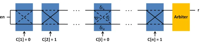
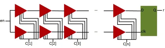
Fig. 1: Arbiter PUF
the arbiter generates a single bit known as the response. Although the nominal delays of direct paths and crossed paths are equal (δia = δid and δib = δic), due to the intrinsic delays of the circuit, different challenges produce different results. The differences between two identical device instances will be sufficient to differentiate the unique responses of the devices.
2.2 Photonic Emission in CMOS
Individual logic gates are implemented on the Complementary Metal Oxide Semiconductor (CMOS) Integrated Circuits (ICs) by a set of connected p-type and n-type Metal Oxide Semiconductor (MOS) transistors. In a static state, where no transistor devices are switching, there is at least one transistor in the off region between the supplied power (VDD) and ground (GND). Therefore, the current consumption of the gate is minimal. However, during a switching event a substantial current passes through the circuit. As a result, the transistors enter an operating region known assaturation for a short period of time. During satu-ration, the kinetic energy of accelerated hot carriers can be released via photon emission [4]. n-type transistors emit significantly more photons as compared to p-type transistors, due to the higher mobility of electrons than holes. Hence, only photons emitted by n-type transistor can be observed in general. The emission rate of the transistors is proportional to the switching frequency of the circuit. However, raising the supply voltage also increases the amount of photons emitted by the device exponentially.
Due to multiple interconnect layers on the frontside of modern IC designs, the optical path is obstructed [23]. Therefore, it is almost impossible to observe pho-tonic emissions from the frontside. However, phopho-tonic emissions can be observed from the IC backside as well. Although, silicon substrate is highly absorptive for wavelengths shorter than the bandgap energy, the silicon substrate is transpar-ent to near infrared (NIR) emissions. Hence, any NIR photons emitted by the device will pass through the silicon substrate and can be observed from the IC backside.
2.3 Programmable Logic Architecture
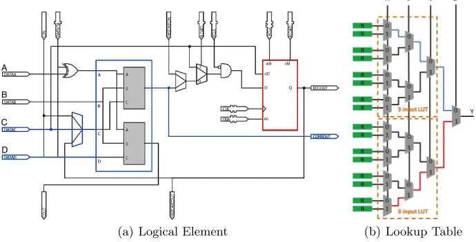
(a) Logical Element (b) Lookup Table
Fig. 2: (a)Architecture of a Logical Element in an Altera MAX V CPLD: A configurable 4-input combinatorial circuit (blue). Additionally each LE consists of multiple control inputs as well as global signals such as clock and enable [2]. (b)The LUT is realized by multiple multiplexers, which are controlled by the data inputs. The output of the LUT is loaded from the existing SRAM cells inside the LUT. In our PUF design, each signal path is connected to one of the LUT’s inputs (input A). The challenge signal is connected to all other three inputs (B, C and D) in order to limit the routing only to two paths inside the LUT.
2.4 Related Work
In recent years, many different attacks on PUFs have been proposed. Settling-state based PUFs, such as SRAM PUFs, can be physically cloned by semi-invasive attacks [10]. The authors of this work demonstrated how SRAM PUF responses can be characterized by a Focused Ion Beam (FIB) circuit edit. More-over, SRAM PUFs are also vulnerable to fully-invasive attacks, due to lack of tamper detection mechanism [20]. It was also shown that timing-based PUFs, such as Ring-oscillator PUFs, are also vulnerable to semi-invasive electromag-netic (EM) side channel attacks [18].
However, to this date, arbiter PUFs are only the target of mathematical modeling attacks. Modeling attacks require a subset of CRPs to build a model on that and predict the PUF response for all possible challenges [12]. One of the first utilized modeling techniques was linear programming to model the timing-based PUF [21]. Machine-learning tools such as Logistic Regression (LR) can also be utilized to model the arbiter PUF successfully [24]. The modeling attacks becomes more difficult by introducing non-linearities to the PUF delays and re-sponses. Two example of non-linear PUFs are Feed-forward arbiter PUFs [13] and XOR-PUFs [32]. However, it has been shown that Feed-forward PUFs are vulnerable to evolutionary algorithm [25]. Moreover, a modeling attack based on higher number of CRPs and power side channel information can be applied successfully to XOR-arbiter PUFs [16]. Other modeling techniques include solv-ing integer equations utilize the CMOS noise as a side channel information or environmental changes as a fault injection technique to model the timing-based PUFs [6, 5].
Photonic emission analysis is introduced as a new side channel attack to analyze security applications on the chip such as cryptographic ciphers [7]. In order to bypass the multiple interconnect layers on the frontside of the chip, photonic emission analysis and photonic fault injection attacks can be conducted from the backside [31, 30]. It has been shown that chips, such as microcontrollers, can be functionally analyzed by their optical emissions during runtime [19]. Simple Photonic Emission Analysis (SPEA) is another approach that can recover the full AES secret key by monitoring access to S-Box [28]. Furthermore, the full AES secret key can be recovered by a similar approach called Differential Photonic Emission Analysis [11].
3
Experimental Setup
3.1 Measurement Setup
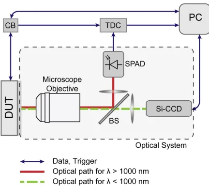
Fig. 3: Controlling the DUT with the CB and capturing emitted photons from the DUT by SI-CCD camera and InGaAs-SPAD
allows long exposure times to accumulate enough photons from the weak hot car-rier emission. Due to the long integration time of several seconds and the limited readout speed of the CCD sensor, it is used for spatial analyses only. The tem-poral analysis of the photonic emission requires a very fast infrared detector. Therefore a free-running InGaAs avalanche detector in Geiger Mode (SPAD) is used to detect single photons. Its sensitivity covers a wavelength range between 1 to 1.6µm with peak quantum efficiency of 20%. Thermoelectrical cooling reduces the dark count rate below 2 kHz.
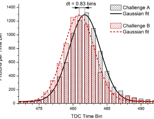
Fig. 4: Timing difference of two different challenges at the output of last stage. The time bin width is 81 ps
resolution by calculating the centroid of the Gaussian-like distribution of the delay time histogram, see Figure 4. This super-resolution technique enhances the time resolution significantly beyond the 81 ps granularity of the TDC and allows measurements of very small shifts in the delay time. Experiments showed that the accuracy of our current setup is limited by drifts in the electronics to 6 ps rms. Apart from the custom made holding of the DUT to a 3-dimensional moving stage and electronics to control and communicate with the CPLD, the setup consists of commercially available components. As the focus of the setup is on time resolved measurements, it can be realized for about 30000 Euros.
3.2 Device Under Test
Fig. 5: Implementation of arbiter PUF by two independent buffers chains.
To further improve the surface quality and optical properties of the devices, an anti reflective coating (ARC) was applied to the devices. Finally, the devices were soldered onto a custom printed circuit board (PCB) to allow capturing of images from the exposed backside of the device while maintaining full electrical connectivity.
3.3 PUF implementation on CPLD
One possibility for implementing arbiter PUFs is to utilize digital multiplexers. In this case, each PUF stage requires two multiplexers. As each multiplexer is realized by a LUT, two inputs out of four available inputs of LUT are utilized, see Figure 2(b). Based on don’t-care inputs, the output of multiplexer can be loaded from different SRAM cells inside the LUT and take different routes to the output. This fact leads to different propagation delays, and consequently, delay imbalances for the two PUF routes. Therefore, due to routing constraints in a LUT of CPLD, we have implemented the stages by two independent LUTs as in [17], see Figure 5. To validate our concept, the design consists of an 8-bit ar8-biter PUF on the CPLD. Each stage is placed manually in an individual LAB on the CPLD to make the PUF chains symmetric. Due to very little delay differences between two chains, the arbiter can sample a meta-stable signal. Moreover, due to asymmetric length of data and clock lines, the delay between the outputs of the last stage and the inputs of the arbiter cannot be designed symmetrically. Hence, instead of using an arbiter, we readout the response by measuring the overall delays of both chains with the help of photonic emission analysis.
4
Measurement Approach
4.1 Optimized Measurement for ordinary MUX-based PUF Characterization
In a MUX-based arbiter PUF, each stage consists of four different propagation delays: two direct path delays and two switching path delays, see Figure 1. In order to completely characterize ann-stage arbiter PUF, all propagation delays of each stage have to be known, hence, 4n delays must be characterized in total. One conceivable way would be to naively measure all 4 propagation delays at all nstages individually by moving the optical setupoverboth inputs and both out-puts of each stage, and simply try both challenge states. However, this technique would require the movement of the chip and adjusting the focus for each move-ment. However, this process could be automated as well, but our measurement setup lacked this capability. As our setup has a very high spatial resolution, a precise aperture movement would be very time consuming, but eventually yield the 4narbiter delays. While practically certainly feasible and also theoretically optimal, we can do much better in terms of physical measurement efforts. A more intelligent solution will simply try to measure the overall propagation de-lays of each PUF chain at the outputs of the very last stage for sufficiently many selected challenge combinations. As the overall delay at the outputs of the last stage is the sum of allndelays in each stage, cf. additive linear model due to [13, 13], every measurement has to consider for every chosen challenge the complete propagation time of two distinct but possible paths — the upper output (D input to sampling flip-flop) and the lower output (C input to sampling flip-flop). If we denote byri the resulting overall time of an individual challenge measurement,
we conclude that we get an inhomogeneous system of linear equations
C·δ=r
for our 4nunknownsδia, δib, δic,andδidand the challenge matrixCwith entries from{0,1}which encode the different valid paths through the arbiter chain. We call a pathci∈ {0,1}4n valid if its respective challenge setting withinCallows
a full signal propagation of length n, i.e., until its very end. By induction the following is easy to see.
Proposition 1. For an arbiter PUF of lengthn≥1 letCbe the(2n+1)×(4n) matrix consisting of all valid paths through the respective arbiter chain. Then rk(C) = 2n+ 2.
Seeing now that we have only 2n+ 2 linear independent equations inC, we need to generate the remaining 2(n−1) linear independent equations to completely solve our system in another way. Thus, we are forced to consider also partial valid paths instead of full propagation paths. Letci ∈ {0,1}4n be a valid path;
for integers 1≤u, v≤na vector of the form
(0, . . . ,0, c4u, c4u+1, c4u+2, c4u+3, . . . , c4v, c4v+1, c4v+2, c4v+3,0, . . . ,0)∈ {0,1}4n
Note 1. For a partial valid path we will measure its signal time only from the inputs of arbiter stageuuntil its output at stagev and deliberately denote this partial time simply also byri.
Including such partial measurementsri (i.e. including measurements within the
arbiter chain) and their corresponding pathsci we also get by induction.
Proposition 2. For an arbiter PUF of lengthn≥1 and its2n+ 2 valid paths (corresponding to the linear independent row vectors) there exist2(n−1) appro-priate partial valid paths such that their combined challenge matrix C has full rank 4n.
This Proposition implies that we only need 2(n−1) partial measurements which we classify with respect touandv into three classes:
1. u= 1 and 1 ≤v < n: Measurement begins at the inputs of the first stage and ends in the middle of the chain.
2. 1< u, v < n: Measurement starts at some inputs in the middle of the chain and also ends in the middle of the chain.
3. 1< u≤nandv=n: Measurement starts at the inputs in the middle of the arbiter chain and and ends after the last stage.
In order to keep the previously discussed physical measurement efforts minimal, it is therefore obvious to generate the missing linear independent equations out of group 1 or 3 — dependent on varying setup advantages. This completes our description of an optimized measurement for a classical MUX-based PUF with nstages.
4.2 Simplified Measurement for delay-based PUFs
As we already pointed out in Section 2.1, we have δia =δid, andδib =δic for their respective buffers. Moreover, as the two paths, i.e., the upper and the lower path are not crossing at all, in other words they are disjoint, we can consider them completely separately, see Figure 5. Towards this, let us consider the upper path and simply denote its n unknown delays by δ1, . . . , δn. I.e., setting the
respective ith challenge bit to 1 adds the delayδ
i to the overall complete signal
propagation time which will be denoted byrj for thejthmeasurement from the
first input until the last output — just through all nstages. If we now define the distinguished variable∆n+1 as the overall complete signal propagation time for setting allnchallenge bits to 0 we get the (already solved) linear system
1 0· · ·0 0 0 1· · ·0 0
..
. . .. ... ... 0 0· · ·1 0 0 0· · ·0 1
· ∆1 ∆2 .. . ∆n
∆n+1
= r1 r2 .. . rn
rn+1
for which we simply require the measurements ri, i = 1, . . . , n+ 1. The lower
path can be handled in an analog way, sayC0·∆0=r0. Moreover, using the unit vectorsei∈ {0,1}n+1,i= 1, . . . , n+ 1, we find that we get from
ei·∆−en+1·∆ =ri−rn+1, and
ei·∆0−en+1·∆0=r0i−r0n+1
the two individual buffer delays δi and δi0 of stage i incurred by setting the
ith challenge bit to 1. We thus conclude that we need only 2n+ 2 “full path” measurements to completely characterize a delay-based PUF withnstages.
5
Results
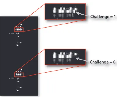
We have chosen the challenge 00000000 as the reference challenge for our mea-surements. In order to measure the effect of each challenge bit, we have tried the challenge combinations with hamming distance one to see the effect of each chal-lenge bit individually. The enable signal was switched with a frequency of 4 MHz and the chip was supplied with 2.2 V. The optical emission of the PUF circuit reveals the position of each stage, see Figure 6. Moreover, the inputs and out-put of each stage for measurement can also be found on this emission image. In case of controlled PUFs, where no electrical access to challenges is available [8], comparing the optical emission of the PUF stages can also reveal the state of individual challenge bits. By changing each challenge bit, the emission pattern of each LE is changed, and therefore, the challenge can be read without any elec-trical access to it, see Figure 7. Therefore, the equations provided in Section 4 can still be used to characterize the PUF by finding challenges with hamming distance one from each other. We repeated the measurement 50 million cycles to capture enough number of photons for analysis. The reference challenge also has been measured multiple times during our experiments to compare the con-sistency of measurements. The measurement results of 8 challenge combinations compared to the reference challenge can be found in Figure 8. Positive timing difference means that the delay is decreased in comparison to reference challenge and vice versa. It can be seen that flipping the challenge bit from 0 to 1, makes in most cases both upper and lower chains faster. Moreover, the timing differ-ences between both chains can also be found in the table. Based on the overall delay difference of two chains, the response can be predicted. In this case, if the timing difference between two chains is positive, the response is 1, otherwise the response is 0.
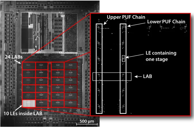
Fig. 6: The backside reflectance image acquired using a laser scan microscope (left). Inside the framed area, all programmable logic cells are located. The grid corresponds to the placement of 4 by 6 LABs with additional routing infras-tructure in-between. Within each LAB, 10 LEs are located (only a single LAB is shown containing the LEs). Optical emission of the 8-bit arbiter PUF on the CPLD (right). Each stage is realized by two LEs in a LAB in parallel.
Fig. 7: Reading challenge bit from the emission image of each LE
6
Discussion
Fig. 8: Measurement results of challenge combinations with hamming distance one (the 8 combinations from the left). Measurement results of set of arbitrary challenge combination (the last 8 combinations from the right). The reference challenge is 00000000.
photons by the detector, is the disadvantage of this methodology. Besides, our attack requires direct physical access to the DUT, while it may not be required by modeling attacks.
Measuring the effect of each challenge takes approximately 12.5 seconds by supplying the chip with 2.2 V and enabling the PUF input with 4MHz frequency. Supplying the chip with 1.8 V, for example, reduces the number of emitted photons by a factor of 3, and the measurement time increases consequently by a factor of 3. However, we can increase the frequency to 100MHz to increase the number of emitted photons and to reduce the measurement time. Furthermore, immersion objectives or objective lenses with larger numerical aperture can be utilized to reduce the measurement time for each challenge to under 1s. Our physical characterization of an arbiter PUF can also find the dominant stages in the chain. Measuring a set of dominant stages can make the response prediction much easier. Therefore, this technique can help to improve the PUF behavior by designing and constructing more balanced routes and stages.
7
Conclusion
response. Although we carried out our experiments on a CPLD PUF implementa-tion, the same methodology can be applied to other hardware implementations. As a result, it is revealed that the timing-based PUFs, specifically arbiter PUFs, are vulnerable to photonic emission analysis.
Acknowledgements. The authors would like to acknowledge the support of the German Federal Ministry of Education and Research in the project PhotonFX and the Helmholtz Research School on Security Technologies.
References
1. Altera: MAX V Device Handbook. Altera Corporation, San Jose (2011)
2. Altera: Quartus II Web Edition Software (2013), http://www.altera.com/ products/software/quartus-ii/web-edition/qts-we-index.html
3. Armknecht, F., Maes, R., Sadeghi, A., Standaert, O.X., Wachsmann, C.: A For-malization of the Security Features of Physical Functions. In: Security and Privacy (SP), 2011 IEEE Symposium on. pp. 397–412. IEEE (2011)
4. Boit, C.: Fundamentals of Photon Emission (PEM) in Silicon – Electrolumines-cence for Analysis of Electronic Circuit and Device Functionality. In: Microelec-tronics Failure Analysis: Desk Reference. p. 356 ff. ASM International (2004) 5. Delvaux, J., Verbauwhede, I.: Fault Injection Modeling Attacks on 65nm
Ar-biter and RO Sum Pufs via Environmental changes. Tech. rep., Cryptology ePrint Archive: Report 2013/619, 2013, https://eprint. iacr. org/2013/619 (2013) 6. Delvaux, J., Verbauwhede, I.: Side Channel Modeling Attacks on 65nm Arbiter
PUFs Exploiting CMOS Device Noise. In: Hardware-Oriented Security and Trust (HOST), 2013 IEEE International Symposium on. pp. 137–142. IEEE (2013) 7. Ferrigno, J., Hlav´aˇc, M.: When AES Blinks: Introducing Optical Side
Chan-nel. Information Security, IET 2(3), 94 –98 (2008),http://dx.doi.org/10.1049/ iet-ifs:20080038
8. Gassend, B., Clarke, D., Van Dijk, M., Devadas, S.: Controlled Physical Ran-dom Functions. In: Computer Security Applications Conference, 2002. Proceed-ings. 18th Annual. pp. 149–160. IEEE (2002)
9. Gassend, B., Clarke, D., Van Dijk, M., Devadas, S.: Silicon Physical Random Func-tions. In: Proceedings of the 9th ACM conference on Computer and communica-tions security. pp. 148–160. ACM (2002)
10. Helfmeier, C., Boit, C., Nedospasov, D., Seifert, J.P.: Cloning Physically Unclon-able Functions. In: Hardware-Oriented Security and Trust (HOST), 2013 IEEE International Symposium on. pp. 1–6. IEEE (2013)
11. Kr¨amer, J., Nedospasov, D., Schl¨osser, A., Seifert, J.P.: Differential Photonic Emis-sion Analysis. In: Constructive Side-Channel Analysis and Secure Design, pp. 1–16. Springer (2013)
12. Lee, J.W., Lim, D., Gassend, B., Suh, G.E., Van Dijk, M., Devadas, S.: A Technique to Build a Secret Key in Integrated Circuits for Identification and Authentication Applications. In: VLSI Circuits, 2004. Digest of Technical Papers. 2004 Symposium on. pp. 176–179. IEEE (2004)
14. Maes, R., Van Herrewege, A., Verbauwhede, I.: PUFKY: A Fully Functional Puf-based Cryptographic Key Generator. In: Cryptographic Hardware and Embedded Systems–CHES 2012, pp. 302–319. Springer (2012)
15. Maes, R., Verbauwhede, I.: Physically Unclonable Functions: A Study on the State of the Art and Future Research Directions. In: Towards Hardware-Intrinsic Secu-rity, pp. 3–37. Springer (2010)
16. Mahmoud, A., R¨uhrmair, U., Majzoobi, M., Koushanfar, F.: Combined Modeling and Side Channel Attacks on Strong PUFs. Tech. rep., Cryptology ePrint Archive: Report 2013/632, 2013, https://eprint. iacr. org/2013/632 (2013)
17. Majzoobi, M., Koushanfar, F., Devadas, S.: FPGA PUF using Programmable De-lay Lines. In: Information Forensics and Security (WIFS), 2010 IEEE International Workshop on. pp. 1–6. IEEE (2010)
18. Merli, D., Schuster, D., Stumpf, F., Sigl, G.: Semi-invasive EM Attack on FPGA RO PUFs and Countermeasures. In: Proceedings of the Workshop on Embedded Systems Security. p. 2. ACM (2011)
19. Nedospasov, D., Schl¨osser, A., Seifert, J.P., Orlic, S.: Functional Integrated Circuit Analysis. Hardware-Oriented Security and Trust (HOST), 2012 IEEE International Symposium on pp. 102–107 (2012)
20. Nedospasov, D., Seifert, J.P., Helfmeier, C., Boit, C.: Invasive PUF Analysis. In: Fault Diagnosis and Tolerance in Cryptography (FDTC), 2013 Workshop on. pp. 30–38. IEEE (2013)
21. Oztiirk, E., Hammouri, G., Sunar, B.: Towards Robust Low Cost Authentication for Pervasive Devices. In: Pervasive Computing and Communications, 2008. Per-Com 2008. Sixth Annual IEEE International Conference on. pp. 170–178. IEEE (2008)
22. Parusi´nski, M., Shariati, S., Kamel, D., Xavier-Standaert, F.: Strong PUFs and their (Physical) Unpredictability: A Case Study with Power PUFs. In: Proceedings of the Workshop on Embedded Systems Security. p. 5. ACM (2013)
23. Rankl, W., Effing, W.: Smart Card Handbook. Wiley, fourth edn. (2010)
24. R¨uhrmair, U., Sehnke, F., S¨olter, J., Dror, G., Devadas, S., Schmidhuber, J.: Mod-eling Attacks on Physical Unclonable Functions. In: Proceedings of the 17th ACM conference on Computer and communications security. pp. 237–249. ACM (2010) 25. R¨uhrmair, U., S¨olter, J., Sehnke, F.: On the Foundations of Physical Unclonable
Functions. IACR Cryptology ePrint Archive 2009, 277 (2009)
26. Sadeghi, A.R., Visconti, I., Wachsmann, C.: Enhancing RFID Security and Privacy by Physically Unclonable Functions. Springer (2010)
27. Schl¨osser, A., Dietz, E., Frohmann, S., Orlic, S.: Highly Resolved Spatial and Tem-poral Photoemission Analysis of Integrated Circuits. Measurement Science and Technology 24(3), 035102 (2013)
28. Schl¨osser, A., Nedospasov, D., Kr¨amer, J., Orlic, S., Seifert, J.P.: Simple Photonic Emission Analysis of AES. In: Cryptographic Hardware and Embedded Systems– CHES 2012, pp. 41–57. Springer (2012)
29. ˇSkori´c, B., Tuyls, P., Ophey, W.: Robust Key Extraction from Physical Uncloneable Functions. In: Applied Cryptography and Network Security. pp. 407–422. Springer (2005)
30. Skorobogatov, S.: Optical Fault Masking Attacks. In: Fault Diagnosis and Toler-ance in Cryptography (FDTC), 2010 Workshop on. pp. 23–29. IEEE (2010) 31. Skorobogatov, S.P., Anderson, R.J.: Optical Fault Induction Attacks. In:
32. Suh, G.E., Devadas, S.: Physical Unclonable Functions for Device Authentication and Secret Key Generation. In: Proceedings of the 44th annual Design Automation Conference. pp. 9–14. ACM (2007)