Comparative Analysis of Ultra Low Power
Based 1-bit Full Adder Using Different
Nanometer Technologies
Anitesh Sharma
1,Ravi Tiwari
2PG Student [VLSI], Dept. of ECE, ShriShankracharya Group of Institution, Bhilai, Chattisgarh, India1
Assistant professor, Dept. of ECE, ShriShankracharya Group of Institution, Bhilai, Chattisgarh, India2
ABSTRACT:Full adder can be designed using CMOS logic, transmission gates, dynamic logic . This paper describes
an Ultra Low Power based one bit full adder.TheUltra Low Power based adder designs considered were SERF adder, GDI adder, 10T adder and 11T adder analyze.All the designs were simulated using Tanner EDA tool v15.0. Simulations were done at 45nm, 32nm technologies. Performance analyses were done with respect to power, delay and power delay product obtained at 45nm, 32nm technologies.
KEYWORDS: Ultra low power, Full Adder, Tanner EDA tool v15.0.
I.INTRODUCTION
CMOS became the most used technology to be implemented in VLSI chips .Digital integrated circuits commonly use CMOS circuits as building blocks. The continuing reduce the area of CMOS circuits and corresponding increase in chip density and operating frequency have made power consumption a major concern in VLSI design. Improve the performance of design VLSI architectures required more efficient arithmetic processing units, which are optimized for the high speed and low power consumption.
The adder is one of the basic elements in many VLSI systems. It plays an important role in many arithmetic units such as multipliers and dividers. Thus, lowering the power consumption of the adders is an important design objective for low power digital designs. For these reason many techniques have been used to reduce power consumption and has become one of the main objective of digital design.Full adder is a basic component for performing arithmetic operation in digital design, digital design underpins the creation of the myriad of imaginative digital devices that surround us. Such devices as digital computers, hand held calculators, microprocessors and so forth.It is very important to choose the adder topology that would yield the desired performance. So improve the performance of the full adder module is the main design objective
Digital circuits operates in subthershold mode for achive ultra low.When gate-to-source voltage (Vgs) is lower then its threshold voltage (Vth) then subthershold current of MOSFET is flow between the source and drain, MOSFET behaves like a bipolar transistor. There are less minority carriers in the channel, but their presence comprises a current and the state known as weak inversion. When Vgs>Vth , in the channel the electron density is greater then the p-type acceptor density in this condition current caused by the drift current the state known as strong inversion. In CMOS design, at weak inversion the current is subthershold parasitic leakage, but if supply voltage is less then threshold voltage the circuit can be operated by using subthershold current due to this reason the circuit achive a low power consumption.
II.LITERATURE SURVEY
MOSFET. In this paper, the proposed circuit has been analyzed for parameters like- power consumption and power delay product.
Authors [2] design the 10-T full adders by using low power XOR gates and multiplexer. This paper describes the new design of full adders perform better as compare to existing 1-bit full adders in terms of power consumption and delay. Purposed 1-bit full adder is having better output swing voltage as compare to GDI based 10-T full adder.
Authors [3] presented the design of low power 1-bit full adder by using XOR pass transistor logic and transmission gate for carry. The power supply is not connected directly to the inputs, for this reason the transition activity and charge recycling capability is to be reduced an given great amount of reduction in power consumption.
Authors [4] designaBranch Based Logic-Pass Transistor Full Adder (BBL-PT FA). This full adder design by using pass transistor based sum block and branch logic style based carry block. In this paper novel design of 1-bit full adder reduced the number of transistor by using same input in two parallel branches in BBL-PT FA. Carry block is modified in this novel design method of full adder.
Authors [5] described a new design of full adder based on pass transistor logic(PTL). The full adder cell design by using degenerate 5-transistor XOR-XNOR module. This method provides the low complexity of circuit, low power consumption and minimum delay.In PTL based full adder, solved the problem of multiple threshold voltage loss by using 5 transistor XOR-XNOR logic module.
Authors [6] purposed a new design of full adder circuit. This is based on XOR-XNOR design full adder circuits in a single unit. Main purpose of this work is to compare the power, delay and power delay product of 1-bit full adder design in different CMOS logic styles. Purposed full adder circuit is compare with the CMOS, Hybrid, Bridge, XOR-XNOR adder circuits in terms of power, delay, PDP. .
Authors [7] presented several low power full adder based on the sense energy recovery full adder (SERF) design and the GDI (Gate diffusion input) technique. These circuits are providedultra low power consumption operating at sub- threshold region.
Authors [8] proposed five hybrid full adder cell are for low power parallel multipliers. The full adders allow NAND gates to generate most of the multiplier partial product bits in the place of AND gates, which is reduce the power consumption and the total number of needed transistors
Authors [9] described the design of a high-speed low-power 1-bit full adder cell. This full adder circuit are focused on the low power consumption and higher speed at low supply voltage. Using pseudo-NMOS together with two inverters reduce the area of the circuit.
Authors [10] design a higher speed full adder cell using 10 transistors. The proposed full adder has the advantage of low power consumption and high operating speed. It reduce the area by using the small number of transistor. The low power consumption is achieved by eliminating the path between source to ground and reducing the internal node of the circuit .
III.PROPOSED FULL ADDERS
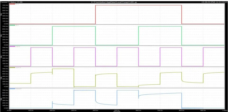
Fig. 1(a) Schematic of SERF
Cout is connected to supply voltage (Vdd) and the SUM signal will equal to difference between supply voltage and thershold voltage. Another problem with this design is when input vector AB="01" or "10" then floating node connected to the ground.WhenCin is high, Cout is charged to supply voltage, but when Cin is low,Cout discharged to thershold voltage of PMOS (Vtp) which is greater thenthershold voltage of NMOS (Vtn) by using PMOS pass transistor. This problem is agitated if the circuit works at subthreshold voltage. If A = “1” , some current flows to Cout node and increases voltage greater then the thershold voltage of PMOS transistor in some cases depending on the sizing of the pass transistors. In this case the Sum signal is dependent on the value of Cin, for instance, if Cin is high, the Sum is equal to difference between supply voltage and thershold voltage cause a problem in subthreshold mode.
Fig. 1(b) Transient Analysis of SERF
Fig. 2(a) Schematic of GDI Full Adder
When the input signal is ABCin=”001”, suppose that the circuit is operating at supply voltage VDD=0.7V and the threshold voltage for PMOS and NMOS circuit are -0.33 and 0.34 respectively. In this case, Fig.2(a), illustrate the problem which is even more degradation at lower supply voltages for the circuit.
Fig. 2(b) Transient Analysis of GDI Full Adder
Full adder design by using two input XOR gates and 2-to-1 multiplexer. Proposed 10T full adder design made by using two 4T XOR gates and one 2-to-1 multiplexer. The Boolean equation of sum and Cout are
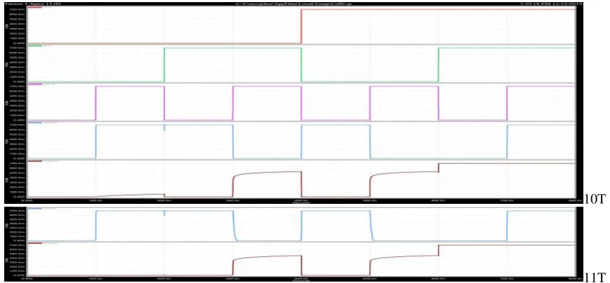
If output voltage is 0.7V or nearest to 0.7V then it shows logic 1 else it shows logic 0. Fig. 3(c) shows the transient analysis of 10T full adder with input combination „000‟ to „111‟. When ABCin=011 or ABCin=101 then value of Cout is 0.5V which is nearest to 0.7V, in that case we assume Cout as a logic 1.
Fig. 3(a) Proposed 10T full adder
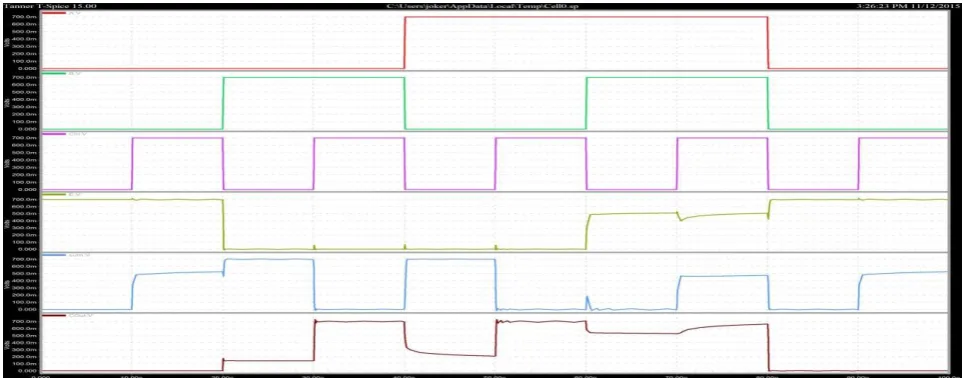
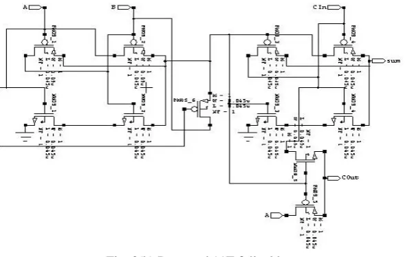
Fig. 3(b) shows the design of proposed 11T full adder, is modified the 10T full adder using an extra transistor MPMOS_6 to improve the performance of full adder.This minimize the power consumption and reduce delay, threshold loss problem and also improve the speed of circuit.
Fig. 3(b) Proposed 11T full adder
10T
11T
Fig. 3(c) Transient analysis of proposed 10T and 11T full adder
IV. RESULT AND DISCUSSION
We have performed simulations of purposed 10T and 11T full adder at 45nm, 32nm technologies with supply voltage 1V, 0.7V respectively, by using Tanner EDA tool 15.0.
Table I
Power consumption, Delay, PDP of Full Adders at 45nm technology
Full Adder cell Power consumption(nW) Delay(ps) PDP(nW*ps)
SERF 241 104 25064
GDI 122 52 6344
Purposed 10T 39.35 45.5 1790
Purposed 11T 36.18 40.72 1473
Different type of full adders obtained power consumption, delay and power delay product as in Table I and Table II. Table I shows the power consumption, delay and power delay product of full adders obtained at 45nm technology with power supply 1V.
Table II
Power consumption, Delay, PDP of Full Adders at 32nm technology
Full Adder cell Power consumption(nW) Delay(ps) PDP(nW*ps)
SERF 230 65 14950
GDI 41 51 2091
Purposed 10T 18.34 41.23 756
Purposed 11T 17.7 36.4 644
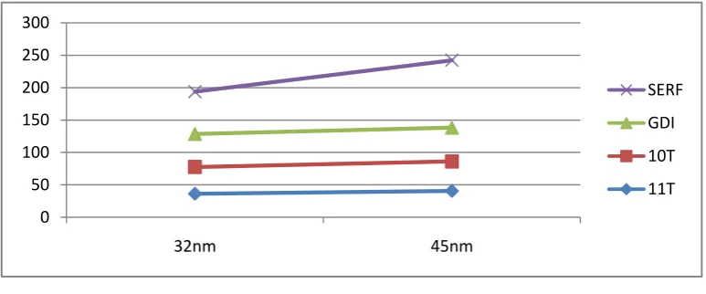
Fig. 4(a) Power Consumption in nW
Fig. 4(a) shows the power consumption of different types of full adders at 45nm and 32nm technologyWhen we reduced area and applying low voltage power supply then power is reduced.. We have seen that power consumption of 11T full adder is lowest as compare to others full adder.
Fig. 4(b) Delay in ps
Fig. 4(b) shows the delay of full adders, when we reduce the channel length of the transistor then delay is also reduced.11T full adder have a minimum delay as compare to others full adder.
V. CONCLUSION
SERF, GDI, 10T and 11T full adder describe in this paper. The result show that the GDI full adder perform better as compare to SERF full adder but at low voltage GDI full adder cannot work properly. At low voltage purposed 10T full adder performed well and consumes low power, reduce delay. Purposed 11T full adder modified structure of 10T by adding extra transistor, which is improve the performance of full adder reduce delay and minimize power consumption. So 11T full adder is best for designing digital systems.
REFERENCES
[1] JagdeepKaurSahani “Design of Full Adder circuit using Double Gate MOSFET” IEEE.Fifth International Conference on Advanced Computing & Communication Technologies 2015, pp. 57-60, 2015.
[2] Gangadhar Reddy Ramireddy“A Novel Power-Aware and High Performance Full Adder Cell for Ultra low Power Design” . International Conference on Circuit, Power and Computing Technologies 2014, pp. 1121-1126, 2014.
[3] Rajesh Parihar“An Implementation of 1-Bit Low Power Full Adder Based on Multiplexer and Pass Transistor Logic”. IEEE International Conference on Information Communication and Embedded System 2014.
[4] JVR Ravindra “Design of Ultra Low Power Full Adder using Modified Branch Based Logic Style”. IEEE European Modelling Symposium 2013, pp. 692-696, 2013.
[5] Jin-Fa Lin “Low Power 10-Transistor Full Adder Design Based on Degenerate Pass Transistor Logic”. IEEE International Symposium on Circuits and Systems 2012, pp. 496-499.
[6] S. Wairya “Ultra Low Voltage High Speed 1-Bit CMOS Adder”. IEEE International Conference on Power, Control and Embedded Systems 2010.
[7] Dag. T. Wisland “Ultra Low Power Full Adder Topologies”. IEEE International Symposium on Circuits and Systems 2009, pp. 3158-3161, 2009.
[8] Z.Abid “Low power multipliers based on new hybrid full adders”. Microelectronics Journal 39 2008, pp. 1509– 1515, 2008.
[9] Amir Ali Khatibzadeh “A 14-Transistor Low Power High Speed Full Adder Cell”. IEEE Canadian Conference on Electrical and Computer Engineering 2003, pp. 163-166, 2008.
[10] Ayman A. Fayed “A Low Power 10-Transistor Full Adder Cell for Embedded Architectures”. IEEE International Symposium on Circuits and Systems 2001, pp.226-229, 2001.
BIOGRAPHY
Mr.Anitesh Sharma is M.E. scholar in Shri Shankracharya Group of Institution, Bhilai, India. His current area of specialization is VLSI Design. He has completed his Bachelors degree from Chhattisgarh Swami Vivekanand Technical University, Bhilai, India in 2013 from Electronics and Telecommunication branch of Engineering.