International Journal of Research
Available at https://edupediapublications.org/journalsp -ISSN: 2348-6848 e-ISSN: 2348-795X Vo lu me 03 Is s u e 13
Sep temb er 2016
Available online:
http://edupediapublications.org/journals/index.php/IJR/
P a g e | 353A New Nested Neutral Point-Clamped (NNPC)
Converter for Medium-Voltage (MV) Power Conversion
Mr. V. Balu &
N. Suresh
Abstract
—In this paper, a new volt age source convert er for medium voltage applications is presented which can op erat e over a wide range of voltages (2.4–7.2 kV) without the need for connect ing t he power semiconductor in series. The operation of t he p rop osed converter is studied and analyzed. In order to cont rol t he p rop osed converter, a space-vector modulation (SVM) strat egy wit h redun - dant switching states has been proposed. SVM usually has redun - dant switching state anyways. What is the main point we are trying t o get to? These redundant switching states help to control the out - p ut voltage and balance voltages of the flying capacitors in the proposed converter. The performance of t he convert er under dif - ferent op erat ing condit ions is invest igat ed in M AT LAB/Simulink environment. The feasibility of the proposed convert er is evaluat ed exp eriment ally on a 5-kVA p rot ot y p e.Index Terms—DC–AC power conversion, multilevel convert er, sp ace vect or modulat ion (SVM ).
I. INT RODUCT ION
MEDIUM-VOLTAGE high-power conversion applications such as motor drives, microgrids, and distributed generation systems use various converter topologies to achieve the desired voltage and performance [1]. Recent developments in semiconductor technology and commercial availability of high-power switches, such as the insulated gate bipolar transis- tor and the integrated gate commutated thyristor, have resulted in a potential acceptance of the two-level voltage source converter (VSC) for high-power applications as well. However, for some applications, e.g., medium voltage drives, HVDC converters, and flexible alternating current transmission system controllers, the voltage ratings of power semiconductor devices are still insufficient to meet the required voltage levels by one single- module of a two-level VSC. Multilevel VSC configurations are the preferred option to meet the desired high voltage and power levels. The main features of these configurations, as compared with the two-level VSC, are their capabilities to reduce: 1) har- monic distortion of the ac-side waveforms; 2)
dv/dt switching stresses; 3) switching losses; and 4) minimize or even eliminate the interface transformer [1]–[5].
The multilevel VSC topologies can be categorized into two groups: classic multilevel topologies and advanced multilevel topologies. The classic multilevel topologies include the neutral- point clamped (NPC), flying capacitor (FC), and the cascaded H-bridge (CHB). [1]. The classic multilevel converters have been commercialized successfully by major manufacturers; however, they have some drawbacks which limit their appli- cations. For instance, the NPC structure with higher number of levels is less attractive because of its limitations which include: 1) higher losses and uneven distribution of losses in the outer and inner devices, 2) dc-link capacitor voltage balance becomes unattainable in higher level topologies with a passive front end when using conventional modulation strategies, and 3) the num- ber of clamping diodes increases substantially with the voltage level. The FC structure needs to have higher switching frequen- cies to keep the capacitors properly balanced, whether a self- balancing or a control-assisted balancing modulation method is used (e.g., greater than 1200 Hz). Also, the number of FCs increases with the voltage level. The CHB structure can reach higher voltage and higher power level with the modular struc- ture; however, this topology needs: a large number of isolated dc sources, an expensive and bulky phase-shifting transformer, and a substantially higher number of active devices to achieve a regenerative option.
A number of variants and new multilevel converters have been proposed in the literature [6]–[16]. These are variations or hybrids of the three classic multilevel topologies and are called advanced multilevel topologies. Among recent proposals, the following topologies have found practical application, which are commercialized by manufacturers: the five-level H-bridge NPC (5 L-HNPC), the three-level active NPC (3 L-ANPC), the five-level active NPC (5 L-ANPC), and the four-level hybrid- clamped converter (4 L-HC). The main features of these con- verters are:
Available online:
http://edupediapublications.org/journals/index.php/IJR/
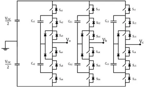
P a g e | 354Fig. 1. Proposed NNPC converter.
transformer which increases the cost and complexity of the converter.
2) A 3L-ANPC is an improved three-level NPC where the neutral clamping diodes are replaced with clamping switches to provide a controllable path for the neutral current, and hence, control the loss distribution among the switches of the converter [10], [11]. This topology distributes the losses between the inner and outer switch- ing devices in each converter leg and thus improves the cooling system design and increases the maximum power ratio of the converter. However, although higher number of the devices as compared to the three-level NPC, the same number of output voltage levels is achieved. This decreases the reliability and increases the cost and com- plexity of the overall converter.
3) A 5L-ANPC is a combination of a 3L-ANPC and 3L-FC, which increases the number of voltage levels [12]–[15]. This converter can reach higher output levels without the need to add series-connected diodes. Moreover, the prob- lem of capacitor voltage balancing when using passive front ends is avoided. This converter, however, is complex as it needs to control the FC voltages and their initial- ization, aside from the NPC dc-link capacitors voltage unbalance control. Another drawback of the 5L-ANPC is that the switch voltage ratings are different in different converter branches (in fact two devices may have to be connected in series for the top and bottom switches). In other words, the voltage stresses of the switches for a 5L- ANPC are different, the outer switches are subjected to half of the dc-link voltage but the inner devices have just 1/4 of the dc-link voltage.
T ABLE I
NUMBER OF ELEMENTS IN DIFFERENT TOPOLOGIES AND THE
PROPOSED TOPOLOGY
4) A 4L-HC converter is an improved ANPC converter that makes four levels at the output voltage [16]. This converter can reach four levels without the need for series-connected power switches and all the switches have the same voltage stress. In comparison to the classic multilevel topologies, although the 4L-HC converter has less number of passive components, it does need two more power switches in each phase which could have a negative impact on the cost and control complexity of the converter.
In this paper, a new multilevel topology, shown in Fig. 1, is presented for medium-voltage high-power application. The proposed converter has the following features:
1) It can operate over a wide voltage range of 2.4–7.2 kV without the need for connecting the power semiconductor in series.
2) It has four levels at the output voltage and unlike afore- mentioned converters, all switches have the same voltage stress (equal to one-third of the dc voltage).
Available online:
http://edupediapublications.org/journals/index.php/IJR/
P a g e | 355T ABLE II
SWITCHING STATES OF THE FOUR-LEVEL NNPC AND CONTRIBUTION OF THE AC-SIDE CURRENTS TO THE FC VOLTAGES
Fig. 2. Space-vector diagram of a four-level converter.
to the four-level FC it has fewer capacitors. In compar- ison to a 4L-HC converter, it has less number of power switches. Also, unlike CHB converters, it does not need to have a transformer for isolated dc sources.
The proposed multilevel converter is studied and analyzed, and a space-vector modulation (SVM) strategy has been devel- oped to control and balance the capacitor voltages. The per- formance of the converter under different operating conditions is investigated in MATLAB/Simulink environment. A 5-kVA laboratory prototype has been built and results are presented.
II. CONVERT ER TOPOLOGY
A. Operation of the Proposed Converter
The proposed multilevel topology, as shown in Fig. 1, is a combination of an FC topology and a NPC topology named nested neutral point-clamped (NNPC) converter which provides a four-level output voltage. To ensure equally spaced steps in the output voltages, the capacitor Cx1 and Cx2 ,x = a,b,c are
Fig. 3. Block diagram for the implementation of the developed SVM-based strategy.
T ABLE III
PARAMETERS OF THE SYSTEM (SIMULATION STUDIES)
Available online:
http://edupediapublications.org/journals/index.php/IJR/
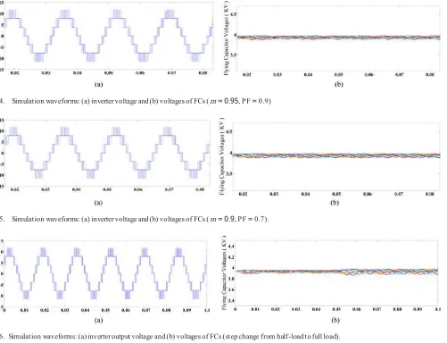
P a g e | 356Fig. 4. Simulation waveforms: (a) inverter voltage and (b) voltages of FCs (m = 0.95, PF = 0.9)
Fig. 5. Simulation waveforms: (a) inverter voltage and (b) voltages of FCs (m = 0.9, PF = 0.7).
Fig. 6. Simulation waveforms: (a) inverter output voltage and (b) voltages of FCs (step change from half-load to full load).
Fig. 7. Simulation waveforms; voltage of FCs with and without an SVM controller
Four output levels are achieved from six distinct switching combinations. The list of switching combinations is shown in Table II. It should be noted that all switch devices are rated to one-third of the dc-link voltage. Another advantage of the proposed converter is the redundancy in switch combination to produce output levels. For example, there are two redundant switching states (as can be seen in Table II) to generate voltage levels of 1/6Vdc and −1/6Vdc . Each redundant state provides a specific charging and discharging current path for each floating capacitor. This is a specific feature of redundant switching states that can be used to achieve voltage balancing of the capacitors.
T ABLE IV
PARAMETERS OF THE SYSTEM (EXPERIMENTAL STUDIES)
The main technical challenge is to identify the best redundant switching state to achieve this.
B. SVM for the Proposed NNPC Converter
Available online:
http://edupediapublications.org/journals/index.php/IJR/
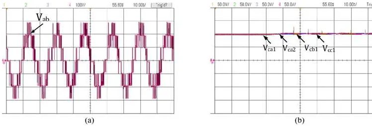
P a g e | 357Fig. 8. Experimental setup for the proposed NNPC converter.
Fig. 9. Experimental results, steady state: (a) inverter output line voltage and (b) voltages of FCs, m = 0.95, PF = 0.9.
Fig. 10. Experimental results, steady state: (a) inverter output line voltage and (b) voltages of FCs, m = 0.9, PF = 0.7.
International Journal of Research
Available at https://edupediapublications.org/journalsp -ISSN: 2348-6848 e-ISSN: 2348-795X Vo lu me 03 Is s u e 13
Sep temb er 2016
Available online:
http://edupediapublications.org/journals/index.php/IJR/
P a g e | 358 . .= . .
1
.
by the three adjacent switching vectors [5], [17] and the can be described as
V˙1 t1 + V˙2 t2 + V˙3 t3 = V˙re f Ts t1 + t2 + t3 = Ts V˙re f =
.
˙re f . j θ
ref
.V . e , θ =< V˙ (1)
where Ts is the switching period, V˙1 , V˙2 , and V˙3 are the three switching vectors adjacent to Vref and t1 , t2 , and t3 are the calculated on-duration time intervals of the switching vectors, respectively [18].
The procedure of the SVM strategy can be summarized in Fig. 3 [18].
In order to achieve voltage balancing for the capacitor, the best switching states should be selected among the available redundant switching state to minimize the voltage deviation of the capacitors. Therefore, a cost function, J , can be defined based on the energy stored in the capacitors as follows:
J = Ja + Jb + Jc
Fig. 12. Experimental results, the effectiveness of the SVM controller to control voltages of the FCs.
where, ¯iC cx i is the averag e value of the Ccx i capacito r curren t. This current can be calculated based on the switching states and their relationship to ac-side currents ia , ib , and ic , as can be seen 2
2 Ccxi
.
VCcxi − Vd c .2
3 in Table II. For different switching states, the average currents and there- x i=1
x = a, b, c. (2)
To minimize the cost function J , the following condition should be satisfied:
2
fore the cost function can be calculated. The switching states which minimize the cost function J , is selected to apply to the converter.
III. SIMULATION RESULTS
dJx = . C .V V
dc . dVCcxi dt
i=1
cxi Ccxi −
3 dt ≤
0
In order to show the performance of the proposed NNPC four-level converter, simulation studies have been done in
where
x = a, b, c (3)
dVCcxi
MATLAB/Simulink environment for a 5-MVA/7.2-kV inverter. The parameters of the system are shown in Table III. The simulation also demonstrates the effectiveness of the developed iCcxi = Ccxi
dt
x = a, b, c (4)
and iCcxi is the current of the capacitor Ccxi,x = a,b,c, i = 1,2. Equation (3) can be rewritten as
2
SVM to generate output voltages, and to regulate and balance the voltage of FCs.
The performance of the proposed NNPC converter and SVM controller has been studied during both the steady-state and transient-state.
. . V
Vdc .i 0, x = a, b, c. (5) A. Steady-State Analysis
i=1 Ccxi − 3
Ccxi ≤
Figs. 4 and 5 show the performance of the proposed converter The best switching states should be found to minimize (5).
If an averaging operator is applied to (5) over a one sampling period
using SVM technique with different load power factors. Fig. 4 shows the inverter output voltage, output currents, and FC volt- ages, where modulation index m = 0.95 and load PF is 0.9.
1 ¸ (k
+1)Ts
2 .
VCcx i −
Vdc .
iCcxi ≤0, x = a, b, c.
Fig. 5 also shows the inverter output voltage, output currents, and FC voltages, where modulation index m = 0.9 and load
International Journal of Research
Available at https://edupediapublications.org/journalsp -ISSN: 2348-6848 e-ISSN: 2348-795X Vo lu me 03 Is s u e 13
Sep temb er 2016
Available online:
http://edupediapublications.org/journals/index.php/IJR/
P a g e | 359 22
(6) PF As can be seen = 0.7. from the Figs. 4 and 5, unlike four-level
If the capacitor voltages is assumed to be constant over one Ts , then
diode-clamped converter that has limitation over voltage bal- ancing with high-load power factor, the proposed converter can
. .
VCcxi −
Vdc .
¸
3
(k +1)Ts
iCcxi ≤0, x = a, b, c (7)
regulate and balance capacitor voltages under various different conditions.
i=1
and consequently
. . V
kTs
Vd c .¯i 0, x = a, b, c (8)
It should be noted that the voltage stress for all the power switches are the same and equal to one-third of the dc input voltage which in this case is 3933 V. This means that for a 7.2-kV inverter, a power switch with the rate of 6500 V can be
i=1 Ccxi − 3
Ccxi ≤
used which is available in the market. This is the main outstand-
ing of the proposed converter which can work with a wide range of voltages (2.4–7.2 kV) without the need for connecting the power semiconductor in series.
A. Transient-State Analysis
In this case, step change from half-load to full load (m = 0.95, PF = 0.95) is considered as indicated in Fig. 6. As observed from Fig. 6, voltages of FCs are maintained at the nominal values.
B. Evaluation of the Control Performance
In order to show the performance of the controller, this simu- lation study has been done. In this case, assume that the NNPC converter is operating under normal condition and suddenly at t = 0.15 s, the SVM controller has been deactivated and at t = 0.3 s, the SVM controller reactivated again. As can be seen from Fig. 7, when the controller is deactivated, the volt- age of capacitors diverges and when the controller reactivates the capacitor voltages start converging. This study shows the performance of the SVM controller.
I. EXPER IM ENT AL RESULTS
The feasibility of the proposed converter is evaluated experi- mentally. Fig. 8 shows the experimental setup for the proposed NNPC converter. The parameters of Table IV were used for experiments as a scaled-down prototype.
Figs. 9 and 10 show the performance of the proposed con- verter under different operating conditions. Fig. 8 shows the inverter output voltage, output currents, and FC voltages, where modulation index m = 0.95 and load PF = 0.9. Fig. 10 also shows the inverter output voltage, output currents, and FC volt- ages, where modulation index m = 0.9 and load PF = 0.75.
Fig. 11 shows the performance of the proposed converter under transient condition when load changes from half-load to full load. Fig. 12 shows the effectiveness of the SVM controller to control voltages of the FCs. As can be seen from Figs. 9 to 12, in all the cases capacitor voltages are well balanced.
II. CONCLUSION
International Journal of Research
Available at https://edupediapublications.org/journalsp -ISSN: 2348-6848 e-ISSN: 2348-795X Vo lu me 03 Is s u e 13
Sep temb er 2016
Available online:
http://edupediapublications.org/journals/index.php/IJR/
P a g e | 360 REFERENCES[1] S. Kouro, M. Malinowski, K. Gopakumar, J. Pou, L. G. Franquelo, B. Wu, J. Rodriguez, M. A. Perez, and J. I. Leon, “Recent advances and industrial applications of multilevel converters,” IEEE Trans. Ind. Electron., vol. 57, no. 8, pp. 2553–2580, Aug. 2010.
[2] B. Wu, High-Power Converters and AC Drives.. Piscataway, NJ, USA: IEEE Press, 2006.
[3] J. Rodriguez, J. Lai, and F. Z. Peng, “Multilevel inverters: A survey of topologies, controls, and applications,” IEEE Trans. Ind. Electron., vol. 49, no. 4, pp. 724–738, Aug. 2002.
[4] J. Rodriguez, S. Bernet, B. Wu, J. Pontt, and S. Kouro, “Multilevel voltage- source-converter topologies for industrial medium-voltage drives,” IEEE Trans. Ind. Electron., vol. 54, no. 6, pp. 2930–2945, Dec. 2007.
[5] M. Saeedifard, P. M. Barbosa, and P. K. Steimer, “Operation and control of a hybrid seven-level converter,” IEEE Trans. Power Electron., vol. 27, no. 2, pp. 652–660, Feb. 2012.
[6] Z. Cheng and B. Wu, “A novel switching sequence design for five-level NPC/H-bridge inverters with improved output voltage spectrum and mini- mized device switching frequency,” IEEE Trans. Power Electron., vol. 22, no. 6, pp. 2138–2145, Nov. 2007.
[7] I. Etxeberria-Otadui, A. L. De Heredia, J. San-Sebastian, H. Gaztaaga, U. Viscarret, and M. Caballero, “Analysis of a H-NPC topology for an AC traction front-end converter,” in Proc. 13th Power Electron. Motion Control Conf., Sep. 1–3, 2008, pp. 1555–1561.
[8] V. Guennegues, B. Gollentz, L. Leclere, F. Meibody-T abar, and S. Rael, “Selective harmonic elimination PWM applied to H-bridge topology in high speed applications,” in Proc. Int. Conf. Power Eng., Energy Elect. Drives, Mar. 18–20, 2009, pp. 152–156.
[9] C. M. Wu, W. H. Lau, and H. Chung, “A five-level neutral-point-clamped H-bridge PWM inverter with superior harmonics suppression: A theoreti- cal analysis,” in Proc. IEEE Int. Symp. Circuits Syst., Orlando, FL, USA, May 30–Jun. 2, 1999, vol. 5, pp. 198–201. [10] T . Bruckner, S. Bernet, and H. Guldner, “The active NPC converter and
its loss-balancing control,” IEEE Trans. Ind. Electron., vol. 52, no. 3, pp. 855–868, Jun. 2005.
[11] O. Apeldoorn, B. Odegard, P. Steimer, and S. Bernet, “A 16 MVA ANPC- PEBB with 6 ka IGCT s,” in Proc. IEEE 40th IAS Annu. Meeting. Ind. Appl. Conf., Oct. 2–6, 2005, vol. 2, pp. 818–824. [12] J. Meili, S. Ponnaluri, L. Serpa, P. K. Steimer, and J. W. Kolar,
“Optimized pulse patterns for the 5-level ANPC converter for high speed high power applications,” in Proc. IEEE 32nd Annu. Conf. Ind. Electron., Nov. 6–10, 2006, pp. 2587–2592.
[13] L. A. Serpa, P. M. Barbosa, P. K. Steimer, and J. W. Kolar, “Five-level virtual-flux direct power control for the active neutral-point clamped mul- tilevel inverter,” in Proc. IEEE Power Electron. Spec. Conf., Jun. 15–19, 2008, pp. 1668–1674.
[14] F. Kieferndorf, M. Basler, L. A. Serpa, J. H. Fabian, A. Coccia, and
G. A. Scheuer, “A new medium voltage drive system based on anpc- 5 l technology,” in Proc. IEEE Int. Conf. Ind. Technol.. Vin˜a del Mar, Chile, Mar. 2010, pp. 605–611.
[15] P. Barbosa, P. Steimer, J. Steinke, L. Meysenc, M. Winkelnkemper, and
N. Celanovic, “Active neutral-point-clamped multilevel converters,” in Proc. IEEE 36th Power Electron. Spec. Conf., Jun. 16, 2005, pp. 2296– 2301.
[16] K. Wang, Z. Zheng, L. Xu, and Y. Li, “A four-level hybrid-clamped converter with natural capacitor voltage balancing using PS-PWM,”
IEEE Trans. Power Electron., vol. 29, no. 3, pp. 1152–1162, Mar. 2014.
[17] N. Celanovic and D. Boroyevich, “A fast space-vector modulation algo- rithm for multilevel three-phase converters,” IEEE Trans. Power Electron., vol. 37, no. 2, pp. 637–641, Mar. 2001.
[18] M. Saeedifard, R. Iravani, and J. Pou, “Analysis and control of DC- capacitor-voltage-drift phenomenon of a passive front-end five-level
con- verter,” IEEE Trans. Ind. Electron., vol. 54, no. 6, pp. 3255–3266, Dec. 2007.
M r. V. BALU was born in India in t he y ear of 1985.He received B.Tech degree in Electrical and Electronics Engineering in the year of 2006 & M.Tech PG in Electrical power systems in the year of 2013 from JNTUH, Hyderabad. He is expert in ControlSystems, Electrical circuits, Power system Subjects. He is current ly working as An Associate Professor in EEE Depart ment in Laqshy a Inst it ut e of T echnology and Sciences, Khammam,T elangana St at e ,India.
mail id: [email protected]

![Fig. 3 [18].The procedure of the SVM strategy can be summarized in In order to achieve voltage balancing for the capacitor, the](https://thumb-us.123doks.com/thumbv2/123dok_us/7786635.1288427/6.594.317.543.133.298/procedure-strategy-summarized-order-achieve-voltage-balancing-capacitor.webp)
