International Journal of Research (IJR)
e-ISSN: 2348-6848, p- ISSN: 2348-795X Volume 2, Issue 08, August 2015Available at http://internationaljournalofresearch.org
A 400
µ
W 3
rdOrder LPF with -5 to 27dB Variable Gain for 3G
Direct Conversion Receiver in 180nm CMOS Technology
Dr. D. Asha Devi
Professor, Department of Electronics and Communication Engineering, Sreenidhi Institute of Science and Technology, Hyderabad
[email protected]
B. Surya Anil Kumar
Department of Electronics and Communication Engineering, Sreenidhi Institute of Science and Technology, Hyderabad
surya.anil92 @gmail.com
AbstractDesign of an ultra low power channel select filter with variable gain for the direct conversion wireless 3G receiver is proposed. Portable wireless communication receiver requires a highly linear and low noise base band filter to achieve good sensitivity. Low power consumption is desirable for Portable systems. The proposed 3rd order continues time low pass filter consists of a pre passive filtering stage followed by an OPAMP stage. The pre passive filtering section with minimum number of resistors and capacitors provides high out band linearity and good spurious free dynamic range (SFDR) of the receiver. The single OPAMP stage provides four pole transfer function and reduces in band noise by the use of Cascode structure. Finally, inclusion of a variable gain stage, improves the system suitability for the practical applications. The simulated results of the proposed filter show 12 dBm of Input referred 3rd order intercept point (IIP3),33 dBm of out of band IIP3, with 2.5MHz 3dB frequency. The circuit shows -5 to 27dB variable gain by consuming 400µW power from 1.8V supply in 180nm CMOS.
Key words: Direct Conversion Receiver (DCR); Low Pass Filter (LPF); Unity Gain Bandwidth (UGB); Out of Band IIP3; In Band IIP3; Common Mode Feedback (CMFB)
INTRODUCTION
The RF signal that is received in direct conversion receiver is first filtered and amplified with a pre- select band pass filter and Low Noise Amplifier respectively. Fortunately, no external channel select filter is required and the base band filter section is responsible for filtering and selecting the desired channel in 3G RF spectrum. The selectivity and linearity requirements of base band filter are more critical than in any other architectures due to the absence of preceding highly linear high Q RF and IF filters. Many papers have been published making new
proposals for the design of these filters and each concentrate on getting high linearity and selectivity. Many topologies have been proposed to design filter such as Gm-C, active-RC, and
Integrated active filters. Design of Op-Amp and trans-conductor is crucial in design of these active filters which are the basic building blocks of analog circuits.
International Journal of Research (IJR)
e-ISSN: 2348-6848, p- ISSN: 2348-795X Volume 2, Issue 08, August 2015Available at http://internationaljournalofresearch.org
occupies an area nearly 0.19mm2. It consumes power of 4.2mW [1].
Yong Chen, Pui-in Mak, Li Zhang, He Qian and Yan Wang proposed filter which is designed using LC elements of fifth order is having 20MHz cut-off frequency. It consists of transistorized LC ladder elements realized by combining source followers with Q enhanced floating differential active inductors [2].
Tien-Yu Lo, Chi-Hsiang [3] proposed a novel four pole filter has been implemented of which two poles are provided by Op-Amp to handle the blockers with a supply of 1V. The four pole filter topology includes an Op-Amp which is given a pole tracking ability to achieve low in band levels, high out of band linearity and low power consumption. Although the power consumption and area occupied are less compared to [1] and [2], there is a significant loss between the input and output signal nearly 10-12dB.
Many filters have been designed but most of them are limited with various trade-offs between power consumption, area occupied on the chip etc. [4]-[15]
The proposed circuit gives Op-Amp an additional capability so that the loss is compensated. A variable gain stage is added to the Op-Amp as the final stage so that not only compensating the loss, the signal can be filtered and boosted. The design of filter is a 4th order transfer function in which two poles are given by the passive stage and remaining is obtained from the Op-Amp that works with a power supply of 1.8V. High in-band and out band linearity is obtained along with low power consumption.
FILTER IMPLEMENTATION
Generally, active RC filter designs require large gain and bandwidth. In order to obtain higher order transfer function, a cascade of bi-quads is to be implemented which require high power. In order to reduce the power consumption, Op-Amp is given pole tracking ability so that two of four poles are obtained through Op-Amp and remaining two from the passive stage of the filter. Op-Amp is designed such that its gain is varied such that the loss occurring up to its preceding stage is compensated so that signal is filtered as well as boosted. The overall design of the proposed filter circuit is given in Fig.1.
Fig.1 Block diagram of 3rd order LPF
Passive stage contains differential RC sections which contribute two poles in overall four pole filter transfer function. This passive stage acts like a pre- filtering stage hence that the signal is conditioned before entering into the Op-Amp circuit such that the noise of Op-Amp will not get added to the external noise so the amplification of noise will be significantly decreased. The circuit of the passive section is shown in Fig.2.
Fig.2 Pre - Passive filtering stage of LPF circuit
Pre-passive filtering stage
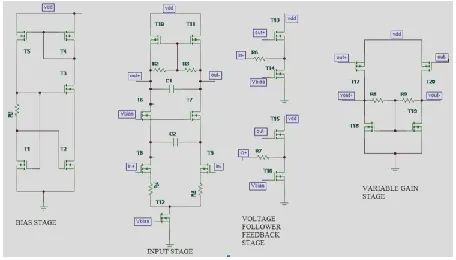
OP - AMP STAGE
Input stage
International Journal of Research (IJR)
e-ISSN: 2348-6848, p- ISSN: 2348-795X Volume 2, Issue 08, August 2015Available at http://internationaljournalofresearch.org
OPAMP IMPLEMENTATION
For the proposed filter circuit in this paper, the op amp should be able to satisfy two aspects. It should be able to provide two poles out of four poles of the complete transfer function of the circuit and the other is the ability to vary its overall gain such that no loss has to be obtained in the signal between input and output. The Op-Amp circuit has a bias generation stage, input stage, and a variable gain stage as a final stage.
For the bias generation stage, constant-Gm bias stage is used in order to generate the bias voltages for the input stage. The poles of the Op-Amp are obtained in the input stage which has capacitors C1 and C2. Degenerated
trans-conductance of the transistors M1 and M2 and
Capacitance C2 provides the necessary UGB. The
other pole frequency is obtained by the trans-conductance of pair of cascoded transistors and capacitor C1. So the DC gain of the Op-Amp is
degenerated trans-conductance of the Op-Amp multiplied by the impedance seen from the Op-Amp output. Overall open loop transfer function of Op-Amp is
0 1 2 0 3,4 1 2 12m GR As sC sCR gm (1)
Where R0 is the output impedance of input stage
of Op-Amp, Gm is the degenerated
trans-conductance of the transistors M1 and M2. Here,
pole frequency formed by C2 is the dominant
pole in the transfer function of Op-Amp. Since, Op-Amp provides a 2nd order transfer function, phase response of Op-Amp should be taken care so that significant margin has to be maintained so that phase response of Op-Amp does not reach
1800. As the phase margin depends on the non-dominant pole of the system, certain value of C1
is selected such that good amount of margin in phase is maintained.
A constant gm bias is used so that, the process
variations do not change the bias voltages hence, accurate response is maintained. Instead of using the error amplifier in common mode feedback circuit, it is simplified by using simple resistive CMFB circuit in order to optimize the power consumption.
The final stage of the Op-Amp circuit is the variable gain stage which is responsible for compensating the signal loss. This stage is composed of differential PMOS common source amplifier stage which gives op-amp a variable gain capability so that it boosts the signal to the required level. The minimum value of R is taken as 1K and maximum value is taken as 50K in this design. Improved in-band and out-band IIP3 can be obtained using this variable gain stage of Op-Amp. The overall filter circuit is shown in Fig.3.
Fig. 3 Op-Amp Schematic
SIMULATION RESULTS
International Journal of Research (IJR)
e-ISSN: 2348-6848, p- ISSN: 2348-795X Volume 2, Issue 08, August 2015Available at http://internationaljournalofresearch.org
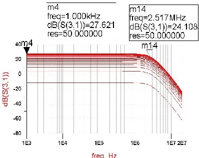
and 31.62MHz are observed as -11.895dBm and -70.238dBm respectively showing the 3 pole roll off in in-band. S21plots are simulated for minimum gain and maximum gain. The minimum value observed as -5.616dB DC gain whose 3dB gain is -9.114dB at 2.5MHz. The maximum gain observed as 27.621dB as DC gain and 3dB gain is 24.108dB at 2.5MHz as shown in Fig.4 and Fig.5 respectively. s21 response for different R values of variable gain stage is shown in Fig.6 which offers a minimum gain of -5.616dB and maximum gain of 27.621dB. Maximum current consumption is observed as 225.57µA is shown in Fig.7. Thus maximum power consumption is 406.026µW with a power supply of 1.8V which is reasonable even the signal is boosted.
Fig. 4 S21 plot for maximum gain
Fig . 5 S21 plot for minimum gain
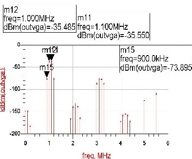
The circuit is subjected to two tone inter modulation test with both in band and out band signals for both minimum and maximum gain. Two -30dBm signals are applied at 1MHz and 1.1MHz for which an in-band IIP3 of 15.663dBm is observed at maximum gain and 23.087dBm of in band IIP3 at minimum gain which shows the better linearity even offering the gain. Plots corresponding to the above analysis are given in Fig.8 and Fig.9. Two -30dBm signals are applied at 10MHz and 21MHz for which out band IIP3 of 46.509dBm is obtained for minimum gain and 34.359dBm for maximum gain giving the best linearity performance for the given test signals.
International Journal of Research (IJR)
e-ISSN: 2348-6848, p- ISSN: 2348-795X Volume 2, Issue 08, August 2015Available at http://internationaljournalofresearch.org
Fig. 7 Transient current plot
Plots corresponding to the above analysis are given in Fig.10 and Fig.11. The overall power consumption of the circuit including the whole Op-Amp is 406.026µW.
Fig. 8 In – band IIP3 for maximum gain
Fig. 9 In – band IIP3 for minimum gain
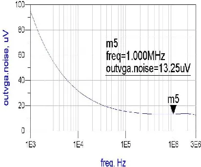
Noise analysis has been done and the plot of the noise spectrum is mentioned in Fig.12. It is observed that there is an input referred in-channel noise of 13.25µV i.e. -97.555dBV.
From the two tone inter-modulation test results, it is observed that
In-band IIP3 = 23.087dBm
Out-of-band IIP3 = 46.509dBm
In-band SFDR is found to be 71.755dBV and out-of-band SFDR is found to be 83.37dBV.
Table.1 Performance Summary of 3rd order LPF
Parameter Simulated Result
CMOS technology
process 180nm
Cut-off frequency 2.5MHz
In – Band IIP3 for
minimum gain -23.087dBm
In – Band IIP3 for
maximum gain 15.663dBm
Out – of – Band IIP3 for
minimum gain 46.509dBm
Out – of – Band IIP3
for maximum gain 34.359dBm
Out – of – Band SFDR 87.37dBV
In – band SFDR 71.755dBV
FoM (Out – of – Band) 1.147× 10⁻³ fJ
FoM (In – Band) 4.17×10⁻² fJ
International Journal of Research (IJR)
e-ISSN: 2348-6848, p- ISSN: 2348-795X Volume 2, Issue 08, August 2015Available at http://internationaljournalofresearch.org
Fig.10 Out – of – band IIP3 for maximum gain
Fig. 11. Out – of – band IIP3 for minimum gain
The figure of merits (FoM) for in-band and out-of-band are found to be
FoM (out-of-band) = 1.147× 10⁻³ fJ
FoM (In-band) = 4.17×10⁻² fJ
The performance summary of the design is mentioned in Table.1.
Fig.12 Input referred in-channel noise spectrum
CONCLUSION
The present study of the proposed research work is design and implementation of 3rd order Butterworth Low Pass Filter is successfully completed with variable gain capability of -5dB to 27dB. The cut-off frequency of the channel selection filter is set to 2.5MHz which makes it suitable for 3G radio frequency specifications. This filter achieves better linearity even at a high gain operation of Op-Amp which is implemented.
REFERENCES
[1.] Mohammad Abdulaziz, Markus Tormanen, Henrik Sjoland, “A 4th order Gm-C filter with 10MHz bandwidth and 39dBm IIP3 in 65nm CMOS(2014)”, IEEE 2014.
[2.] Jose Leopoldo Lopez Ochoa, Esteban Martinez Guerrero, Esdras Juarez Hernandez, “A 3rd OTA-C low pass filter for WCDMA standard applications in zero-IF receiver”, IEEE 2013.
International Journal of Research (IJR)
e-ISSN: 2348-6848, p- ISSN: 2348-795X Volume 2, Issue 08, August 2015Available at http://internationaljournalofresearch.org
receiver in 55nm CMOS”,IEEE transactions on VLSI systems, vol.22, no. 5, MAY 2014. [4.] Jayanth N. Kuppambatti, Baradwaj
Vigraham, Peter R Kinget, “A 0.6V 70MHz 4th order CT Butterworth filter with 55.8dB SNR, 60dB THD at +2.8dBm output signal power”, ISSCC, 2014.
[5.] Yong chen, pui-In Mak, Li Zhang, He Qian and Yan Wang, “A fifth order 20MHz transistorized LC ladder LPF with 58.2dB SFDR, 68-µW/pole/MHz efficiency, 0.13 sq.mm die size in 90nm CMOS”, IEEE transactions on circuits and systems-II, vol.60, no.1, January 2013.
[6.] Kuan Bao, Xiangning Fan, Zhigong Wang, “A 0.18µm CMOS low power reconFigurable low pass filter for multi standard receivers”, 2013 IEEE conference on advanced technologies for communications. [7.] A. Pezzotta, M. De Matties, S.D. Amico
and A Baschirotto, “A CMOS 28nm 880MHz 4th order low pass active RC filter for 60GHz transceivers (2013)”, IEEE 2013.
[8.] Rakesh Kumar Palani, Martin sturm, Ramesh Harzani, “A 1.56mW 50MHz 3rd order filter with current mode active RC bi-quad and 33dBm IIP3 in 65nm CMOS”, IEEE Asian solid state circuits conference 2013.
[9.] Liu junbo, Fan Xiangning, Bao kuan, “A 4th order active Gm-C low pass filter with RC time constant auto tuning for reconFigurable wireless receivers”, IEEE 2013.
[10.] Mostafa Savadi Oskooei, Nasser Masoumi, Mahmud Kamarei and Henrik Sjoland, “A CMOS 4.35mW +22dBm IIP3 continuously tunable channel select filter for WLAN/ WiMAX receivers”, IEEE journal of solid state circuits, vol. 46, no. 6, June 2011. [11.] Antonio liscidini, Alberto Pirola, Rinaldo
Castello, “A 1.25mW 75dB SFDR CT filter
with in band noise reduction”, IEEE solid state circuits conference, 2009.
[12.] Tien-Yu Lo, Chung Chih Hung, “Multimode Gm-C filter for mobile applications in 1-V supply volatge”, IEEE transactions on circuits and systems-II:Express Breifs, vol. 55,no. 4, April 2008.
[13.] Atsushi Yoshizawa, Yannis Tsividis, “A blocker vigilant channel select filter with adaptive IIP3 and power dissipation”, ISSCC 2006.
[14.] Hussain A. Alzehar, Hassan O. Elwan, Mohammed Ismail, “A CMOS highly linear channel select filter for 3G Multistandard Integrated Wireless Receivers”, IEEE journal of solid state circuits, vol. 37, no. 1, January, 2002.
[15.] K. Radhakrishna Rao, S. Srinivasan, “A bandpass filter using Operational amplifier pole”, IEEE journal of solid state circuits, June 1973.
[16.] Ville Saari, Jussi Ryynanen, Saska Lindfors, “Continuous time low pass filters for integrated wideband receivers”, Springer.// [17.] T. Deliyannis, Yichuang Sun, J.K. Fidler,
“Continuous time active filter design”, CRC press.//
[18.] Behzad Razavi, “Design of analog MOS integrated circuits”, Mc GrawHill International Edition 2001.
International Journal of Research (IJR)
e-ISSN: 2348-6848, p- ISSN: 2348-795X Volume 2, Issue 08, August 2015Available at http://internationaljournalofresearch.org
Authors:
D. Asha Devi (M’ 09) received the A. M. I. E. T. E. in 2000 and
M.Tech. degree in Digital Systems and Computer Electronics from JNTU Anantapur in 2005. She was awarded Doctoral degree in 2011 for the contribution of her research work in Embedded System based Instrumentation from S.K.U. Anantapur. She has 13+ years of teaching experience in UG and PG courses in Electronics and Communications Engineering. Her interested fields are design of VLSI and Embedded systems, wireless sensors and FPGA based Embedded Systems.
B. Surya Anil Kumar has received his B. Tech degree in Electronics and Communications Engineering in 2013 from PVP Siddhartha Institute of Technology. He is pursuing his masters in VLSI and Embedded Systems from Sreenidhi Institute of Science and Technology. He completed his PG research work in analog circuit design using Cadence Virtuoso and ADS tools. His research interests are RFIC design, Analog