A MULTIMODE INTERFERENCE COUPLER WITH EXPONENTIALLY TAPERED WAVEGUIDE
J.-J. Wu
Department of Physics
Shandong University of Technology
No. 12 ZhangZhou Road,Zibo,Shandong Province,P. R. China
Abstract—An exponentially tapered structure is introduced into multimode interference (MMI) devices. Compared with a parabolically tapered structure,which has been successfully used in MMI devices, this structure can further reduce the length of these devices. The performances of the 1 × 2 MMI coupler with exponentially tapered structure,such as the optical transmission,the wavelength response and the fabrication tolerance,are investigated by the 2D finite difference beam propagation method. Results show that the exponentially tapered MMI coupler exhibits a similar property to that with a parabolically tapered structure.
1. INTRODUCTION
investigated [8–10]. In [11],we propose another exponentially tapered structure for the same purpose. The use of exponential tapers for the design of more ultracompact 4×4 MMI photonic switch has been reported [12]. But such kind of tapered waveguide is just a special example of our proposed exponentially tapered structure. Compared with the parabolically tapered,which has been successfully used in the MMI devices,this structure can further reduce the length of the MMI devices. In this article,a detailed analysis of the performance of this kind of MMI devices is presented. It is shown that the performance of the MMI couplers with the exponentially tapered structure is similar to the devices with the parabolically tapered structure.
Many numerical approaches have been developed to analyze general dielectric waveguides in different aspects [13–26]. Compared with other numerical techniques,the beam propagation method (BPM) which automatically includes the effects of both guided and radiating fields as well as mode coupling and conversion,is the most popular and powerful numerical technique for modeling guided-wave photonic devices and most commercial software for such modeling is based on it [26]. To date numerous algorithms for BPM have been proposed and successfully applied to a very wide class of dielectric optical waveguide structures. In this paper,the 2D finite difference beam propagation method (FD-BPM) is used in the simulation.
2. THEORY
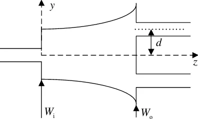
The 1×2 MMI coupler is composed of a single-mode input waveguide, a multimode waveguide,and two single-mode output waveguides. The structure of the compact tapered 3-dB MMI coupler is illustrated in Figure 1. In Figure 1, d is the offset for output waveguides from the
i
W Wo
y
z d
center of the multimode waveguide. The multimode waveguide width is exponentially tapered according to
W(z) = Wi+A
exp
gz LMMI
−1
(1)
A = (Wo−Wi)/(exp (g)−1) (2)
wherezis the direction of propagation of the light,LMMIis the length
of the tapered MMI section, Wi is the width of the MMI section at
z = 0 and Wo is that at z =LMMI,and g is a parameter associated
with the shape of the profile. The input waveguide is located at the center of the start wall of the tapered MMI section,and the two output waveguides are located at Wo/4 and 3Wo/4,respectively,on the end
wall of the tapered MMI section. For Eq. (1),if g is ln(Wo/Wi),then
the tapered structure here mentioned become the exponential structure which has been used [12].
Assuming the multimode waveguide supports m lateral modes with mode numbersv= 0,1,2, . . . , (m−1) at a free space wavelength λ,the effective index of the multimode waveguide section and the lateral confinement section is nr and nc. According to the dispersion
equation,the lateral wave number,kvy,and the propagation constant
βv are related as follows
k2vy+βv2 =k02n2r (3)
where, k0 = 2π/λ, kvy = (v+ 1)π/We(z),and We(z) is the effective
width of the MMI section
We(z) =W (z) +Wg (4)
The Gooss-H¨anchen shift Wg is determined by
Wg =
λ
π nc
nr
2σ
n2r−n2c
−1/2
(5)
whereσ= 0 for transverse electric (TE) mode andσ = 1 for transverse magnetic (TM) mode.
The propagation constantsβv can be deduced from Eq. (3)
βv ≈k0nr−
(v+ 1)2πλ 4nrWe2(z)
(6)
given by
∆φ = (β0−βv)LMMI=
LMMI
0
(β0−βv)dz
= v(v+ 2) πλ 4nr
LMMI
0
dz W2
e (z)
(7)
Substitute Eqs. (1),(2),(4) and (5) into Eq. (6) yields
β0−βv =
v(v+ 2)πλγ 4nrWo2
(8)
where
γ = W
2 o
(Wg+Wi−A)2
− Wo2
g(Wg+Wi−A)2
ln Wg+Wo Wg+Wi
− Wo2(Wo−Wi)
g(Wg+Wi−A) (Wg+Wo) (Wg+Wi)
(9)
The beat length,Le
π,of the two lowest-order modes is
Leπ = π β0−β1
= 4nrW
2 o
3γλ (10)
For the parabolically tapered structure,the beat length of the two lowest-order modes can similarly obtained
Lpπ = π β0−β1
= 4nrW
2 o
3αλ (11)
where
α= W
2 o
2 (Wg+Wi) (Wg+Wo)
+W
2
o tan−1[(Wo−Wi)/(Wg+Wi)]1/2
2 (Wo−Wi)1/2(Wg+Wi)3/2
(12)
For the structure shown in Figure 1,the input single-mode waveguide is located at the center of the start wall of tapered MMI section,and only even-symmetric modes are excited in the tapered MMI section. Then two symmetric interference images can be formed,with a length of
LiMMI= (3/8)Lπ (13)
Comparing (10) and (11),we can see the difference of the beat length of the two lowest-order modes between the parabolically and the exponentially tapered structure. The beat length has relationship with the parametersγ and α. Obviously,the larger the value of γ (or α) is,the shorter the length of the MMI section is. Figure 2 illustrates profiles of γ and α as a functions of the normalized width variation dΩ, dΩ = (Wo−Wi)/Wo,for TE mode. In our calculation,a value
of nr = 1.47 and nc = 1.40 is chosen,the width of the tapered MMI
section at z = LMMI, Wo,is 24µm,and g is 5. It can be seen from
Figure 2, γ is larger than α. Then for the MMI couplers with same width at the start wall and the end wall of the tapered MMI section, the length of MMI section with exponential taper is shorter than the length of that with parabolic taper. It is very favorable for realizing of ultracompact MMI devices. So this exponentially tapered structure will be a good candidate compared with the parabolically tapered structure,which has been successfully used in many MMI devices.
Figure 2. γ and α versus the normalized width variation.
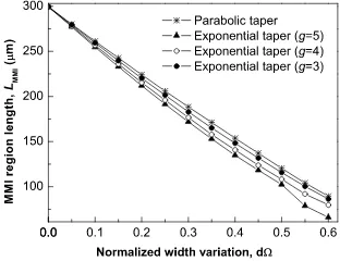
Figure 3. Variation of the MMI length for a tapered MMI coupler with the normalized width.
3. NUMERICAL SIMULATION AND RESULTS
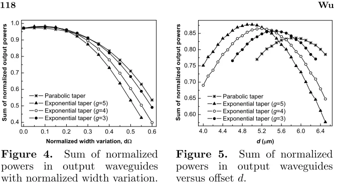
Figure 4. Sum of normalized powers in output waveguides with normalized width variation.
Figure 5. Sum of normalized powers in output waveguides versus offset d.
The Variation of the MMI length for a 3-dB tapered MMI coupler with the normalized width is shown in Figure 3. For each dΩ,the imaging length,LMMI,is obtained via a series of simulations in which
LMMI is allowed to vary in order to maximize the total power,defined
as the sum of the powers in each of the output ports. The sum of the powers at this particular imaging length of the device at each value of dΩ is also presented in Figure 4. As can be see from the Figure 3,the parabolically tapered structure gives the longest devices, as expected,for all the normalized width variation values except at dΩ = 0,and the exponentially tapered structure with g = 5 yield the shortest devices length. For all the tapered MMI devices,the imaging lengthLMMI varies approximately linearly withdΩ as show in
Figure 3. The properties of optical transmission of the MMI devices with different tapered structure as a function of the normalized width variation are similar (see Figure 4). The transmission losses increase with dΩ. But the loss rate is different for these devices. Though the exponentially tapered structure with g = 5 has the lowest imaging length,it has the largest transmission loss when thedΩ exceeds 0.2.
In above simulation,the location of the output waveguides keeps at Wo/4 and 3Wo/4,i.e.,offset d = 6µm. The location of the
the smallest transmission loss. We can also see from Figure 5,for each optimum output waveguide location,the sum of output powers of the exponentially tapered MMI devices is larger than the sum of that of the parabolically tapered MMI device.
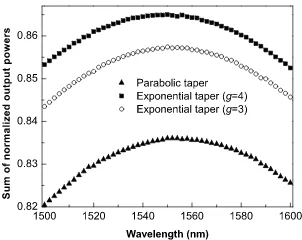
Furthermore,the wavelength response characteristics of the tapered MMI devices at dΩ = 0.4 are also obtained and shown in Figure 6. In our calculation,the optimum output waveguide location and the practical imaging length are used. The results show that the MMI devices with the exponentially tapered structure and the parabolically tapered structure have the same wavelength response characteristics.
Next,the width tolerances for the tapered MMI devices are also investigated and the sum of output powers with the width variation ∆W is shown in Figure 7. In our calculation,both the initial withWi
and the end widthWoof MMI section vary simultaneously. The results
show that all of the examined devices exhibit same width tolerances sensitivity to the width variation. It can also be noticed that all the examined devices are fond to be less sensitivity to the positive width variation. So,during the devices fabrication,enlarging the width of the tapered MMI devices can’t have large influence on the performance of the tapered MMI devices.
Figure 6. Wavelength response for tapered MMI devices.
Figure 7. Fabrication tolerance for tapered MMI devices.
4. CONCLUSION
the MMI devices,this structure can further reduce the length of the MMI devices. The results of the simulation given by the wide-angle finite difference beam propagation method (FD-BPM) show that the performance of the MMI couplers with the exponentially tapered structure is similar to the devices with the parabolically tapered structure. As a result,the exponentially tapered structure will be a good candidate compared with the parabolically tapered structure.
REFERENCES
1. Soldano,L. B. and E. C. M. Pennings,“Optical multimode interference devices based on self-imaging: Principles and applications,” J. Lightw. Technol.,Vol. 13,No. 4,615–627,1995. 2. Levy,D. S.,R. Scarmozzino,Y. M. Li,and R. M. Osgood,Jr.,“A new design for ultracompact multimode interference-based 2×2 couplers,” IEEE Photon. Technol. Lett.,Vol. 10,No. 1,96–98, 1998.
3. Levy,D. S.,R. Scarmozzino,and R. M. Osgood,Jr.,“Length reduction of taperedN×N MMI devices,”IEEE Photon. Technol. Lett.,Vol. 10,No. 6,830–832,1998.
4. Levy,D. S.,K. H. Park,R. Scarmozzino,R. M. Osgood,Jr., C. Dries,P. Studerkov,and S. Forrest,“Fabrication of ultracompact 3-dB 2×2 MMI power splitters,” IEEE Photon. Technol. Lett.,Vol. 11,No. 8,1009–1011,1999.
5. Wei,H. Z.,J. Z. Yu,Z. L. Liu,X. F. Zhang,W. Shi,and C. S. Fang,“Fabrication of 2×2 tapered multimode interference coupler,”Electron. Lett.,Vol. 36,No. 19,1618–1619,2000. 6. Wei,H. Z.,J. Z. Yu,Z. L. Liu,X. F. Zhang,W. Shi,and
C. S. Fang,“Fabrication of 4×4 tapered MMI coupler with large cross section,” IEEE Photon. Technol. Lett.,Vol. 13,No. 5,466– 468,2001.
7. Wei,H. Z.,J. Z. Yu,X. F. Zhang,and Z. L. Liu,“Compact 3-dB tapered multimode interference coupler in silicon-on-insulator,”
Opt. Lett.,Vol. 26,No. 12,878–880,2001.
8. Wei,H. Z.,J. Z. Yu,Z. L. Liu,X. F. Zhang,W. Shi,and C. S. Fang,“Signal bandwidth of general N × N multimode interference couplers,” J. Lightw. Technol.,Vol. 19,No. 5,739– 745,2001.
10. Themistos,C.,M. Rajarajan,B. M. A. Rahman,S. S. A. Obayya, and K. T. V. Grattan,“Rigorous comparison of parabolically tapered and conventional multimode-interference-based 3-dB power splitters in InGaAsP/InP waveguides,”Appl. Opt.,Vol. 43, No. 27,5228–5235,2004.
11. Wu,J. J.,B. R. Shi,and M. Kong,“Exponentially tapered multi-mode interference couplers,”Chin. Opt. Lett.,Vol. 4,No. 3,167– 169,2006.
12. Chang,W. C.,C. H. Lien,P. J. Tsai,and H. J. Wang,“An ultracompact 4×4 photonic switch based on tapered multimode interference,” The 11th IEEE International Symposium on Electron Devices for Microwave and Optoelectronic Applications (EDMO 2003),267–272,Orlando,Florida,USA,November 2003. 13. Watanabe,K. and K. Kuto,“Numerical analysis of optical waveguides based on periodic fourier transform,” Progress In Electromagnetics Research,PIER 64,1–21,2006.
14. Faryad,M. and Q. A. Naqvi,“Fractional rectangular waveguide,”
Progress In Electromagnetics Research,PIER 75,383–396,2007. 15. Chang,H.-W. and M.-H. Sheng,“Field analysis of dielectric
waveguide devices based on coupled transverse-mode integral equation — Mathematical and numerical formulations,”Progress In Electromagnetics Research,PIER 78,329–347,2008.
16. Zhou,X. and G. W. Pan,“Application of physical spline finite element method (PSFEM) to fullwave analysis of waveguides,”
Progress In Electromagnetics Research,PIER 60,19–41,2006. 17. Talebi,N. and M. Shahabadi,“Application of generalized
multipole technique to the analysis of discontinuities in substrate integrated waveguides,” Progress In Electromagnetics Research, PIER 69,227–235,2007.
18. Talebi,N. and M. Shahabadi,“Analysis of a lossy microring using the generalized multipole technique,” Progress In Electromagnet-ics Research,PIER 66,287–299,2006.
19. Dwari,S.,A. Chakrabarty,and S. Sanyal,“Analysis of linear tapered waveguide by two approaches,” Progress In Electromagnetics Research,PIER 64,219–238,2006.
21. Hernandez-Lopez,M. A. and M. Quintillan-Gonzalez,“A finite element method code to analyse waveguide dispersion,” Journal of Electromagnetic Waves and Applications,Vol. 21,No. 3,397– 408,2007.
22. Ooi,B. L. and G. Zhao,“Element-free method for the analysis of partially-filled dielectric waveguides,”Journal of Electromagnetic Waves and Applications,Vol. 21,No. 2,189–198,2007.
23. Park,J. K.,J. N. Lee,D. H. Shin,and H. J. Eom,“Full wave analysis of a coaxial waveguide slot bridge using the Fourier transform technique,” Journal of Electromagnetic Waves and Applications,Vol. 20,No. 2,143–158,2006.
24. El Sabbagh,M. A. and M. H. Bakr,“Analytical dielectric constant sensitivity of ridge waveguides filters,”Journal of Electromagnetic Waves and Applications,Vol. 20,No. 3,363–374,2006.
25. Khalaj-Amirhosseini,M.,“Analysis of longitudinally inhomoge-neous waveguides using Taylors series expansion,”Journal of Elec-tromagnetic Waves and Applications,Vol. 20,No. 8,1093–1100, 2006.