Temperature Performance of GaInNAs-Based Photonic Crystal
Waveguide Modulators
Giovanna Cal`o1, *, Dimitris Alexandropoulos2, and Vincenzo Petruzzelli1
Abstract—The temperature performances of GaInNAs-based semiconductor devices, for next generation communication networks and photonic integrated circuits, are investigated. In particular, GaInNAs-GaInAs Multi Quantum Well active ridge waveguides, patterned with a periodic one-dimensional grating and an active defective region placed in the central layer, have been designed for efficient active optical switches and modulators. The switching mechanism was obtained around the Bragg wavelength λ∼= 1.2896µm at room temperature T = 298 K by properly designing the periodic grating and changing the injected current density from JOF F = 0 mA/µm2 to JON = 0.496 mA/µm2. The proposed device exhibits high performances in terms of crosstalk, contrast ratio, and modulation depth. The temperature performance of the proposed device is analyzed in the rangeT = 298 K–400 K, showing a good stability of the figures of merit: crosstalk CT, contrast ratio CR, and bandwidth ∆λ. In particular, the CT varies at about 1.2 dB in the whole temperature range, whereas CR and ∆λ
experience, respectively, a maximum variation of 25% and 30% of their maximum values.
1. INTRODUCTION
The need of innovative devices, which can guarantee low-cost and low power-budget operation together with high transmission performances, is becoming more and more urgent in telecommunication networks. A major challenge is the achievement of a stable temperature operation not only for laser sources, but also for modulators, switches and routing devices. In particular, photonic integrated networks would benefit the cooler-less operation either for the overall power budget or for the stability of resonance based devices. This issue becomes particularly relevant in applications such as the photonic networks on chip (NoC) [1, 2]. These integrated networks are particularly promising to overcome the performance limitations of on-chip electrical networks, but their behavior is strongly affected by the temperature since the routing devices are generally based on resonance mechanisms which require precise tuning. The temperature constraint can be relieved by design approaches exploiting wide-band operating devices, by compensating the refractive index variation through the inclusion of suitable thermo-optic materials (e.g., negative thermo-optic polymers), or by external temperature stabilization with a non-negligible contribution on the overall power budget [3–6]. Similarly, medium distance and high density optical networks would indeed benefit of low-cost and low-power transmitters modules which can guarantee high bit-rate and stable performances.
In this context, active components based on novel material systems such as GaInNAs, also known as dilute nitrides, appear to be very attractive to achieve stable temperature operation [7, 8]. These materials realize very good electron confinement in the active region and, thanks to a large conduction band offset, lead to lasers with excellent high-temperature performance and uncooled operation in a wide temperature range (e.g., up to 110◦C) [9–13]. Dilute nitrides proved advantageous in different applications in optical communication systems such as Semiconductor Optical Amplifiers (SOA) [14],
Received 24 September 2015, Accepted 16 December 2015, Scheduled 16 April 2016 * Corresponding author: Giovanna Cal`o ([email protected]).
1 Dipartimento di Ingegneria Elettrica e dell’Informazione — Politecnico di Bari, Via Re David n. 200, Bari 70125, Italy. 2Department
optical active switches [15], vertical-cavity surface-emitting lasers (VCSELs) [16], ridge lasers [17], and disk lasers [18].
This paper focuses on the temperature performance of GaInNAs-based semiconductor devices, for next generation communication networks and photonic integrated circuits. In particular, the temperature performance of an active one-dimensional Photonic Crystal (PhC) is investigated. The structure under study consists of a GaInNAs-GaInAs Multi Quantum Wells (MQW) ridge waveguide patterned with a periodic one-dimensional (1-D) grating, which behaves as a modulator by suitably changing the injected current in the active region. The device conjugates the dilute nitride properties to the capability of periodic structures of tailoring the light propagation. In fact, thanks to the induced photonic band gap (PBG), periodic structures can be exploited for the realization of optical devices such as waveguides, cavities, filters [19–22]. Moreover, the PBG devices are even more interesting when exploiting different material properties, e.g., in the case of liquid crystal infiltration or non-linear materials [23, 24], which allow the realization of efficient tunable filters and frequency converters. Moreover, they exhibit a more efficient interaction between the light and the active materials, thanks to their capability of reducing the group velocity at certain wavelengths [25, 26].
Here, we investigate the temperature behavior of periodic waveguiding structures, that we previously proposed at ambient temperature [15, 27–29], for modulation applications in the second window of the fiber optics telecommunications. For this purpose, the numerical model of the active material as a function of temperature is introduced in the Bidirectional Beam Propagation Method based on Method of Lines (MoL-BBPM) simulations.
2. BRIEF THEORY
To account for the interaction of the injected current with the electronic structure of Ga0.77In0.23N0.03As0.97/Ga0.8In0.2As QWs, the rate equations have been introduced. In particular, the following stationary expression is applied [26, 29]:
De∇2σ(x, y, z) =−J(z)
e da
+ gm(x, y, z, σ)
e h v Γ|E(x, y, z)|
2
+Aσ+Bσ2+Cσ3. (1)
where σ(x, y, z) is the charge density distribution; da is the active layer thickness; |E(x, y, z)|is the
electric field modulus; h = 6.626·10−34J·s is the Planck constant; e= 1.602·10−19C is the electron charge; the producthνis the photon energy expressed in eV;J is the injected current density; Γ = 0.044 is the optical confinement factor. Moreover, A= 2·108s−1, B = 7·10−17m3s−1; C = 4·10−41m6s−1 are the non-radiative, radiative, and Auger recombination coefficients, respectively;De = 0.001 m2s−1is
the diffusion coefficient. The material gaingm(x, y, z, σ, λ, T), which depends on the spatial coordinates
x, y, z, the carrier density σ, the wavelength λ, and the temperature T, has been evaluated in the context of Fermi’s Golden Rule (FGR) accounting for intraband effects through a Lorentzian broadening function. The conduction band electronic states, involved in the calculation of the material gain, are given by the Band Anticrossing Model that accounts for theN-induced nonparabolicity of the conduction band, whereas the valence band states are described by a 6×6 LK Hamiltonian. Strain effects are described using the Pikus-Bir Hamiltonian. The gain and bandstructure calculations including strain effects follow the formalism of [30–33]. The temperature influence on the bandgap of the semiconductor structure is accounted for the following expression [34]:
Eg(x, T) = 0.42 + 0.625x− (
5.8
T + 300− 4.19
T + 273
)
10−4T2x−4.19·10
−4
T + 271 + 0.475x
2. (2)
derived for the bandgap calculation of the matrix semiconductor GaxIn1−xAs.
In the rate Equation (1) the propagating electric field E has been calculated by implementing an appropriate version of the MoL-BBPM [35–37]. It allows for accounting the electromagnetic (EM) field along the structure by means of a step by step propagation technique, thus allowing for the injection current in the active layers. Moreover, in presence of dielectric discontinuity this algorithm solves both the forward (+z) and the backward (−z) propagations along the longitudinal z direction of the waveguiding structure. The MoL-BBPM procedure, applied iteratively by evaluating the whole electromagnetic field in the structure, stops when the change of the electromagnetic field, at the generic
The influence of the active layer of Ga0.77In0.23N0.03As0.97/Ga0.8In0.2As QWs on the MoL-BBPM propagation solver is accounted by considering in the iterations the updated values of the complex refractive indexna(x, y, z) in the active layer given by [38]:
na(x, y, z) =np+βeσ(x, y, z) +j
gm(x, y, z, σ, λ, T)
2k0
(3)
wherenp is the refractive index of the active medium in the absence of charge injection,k0 the vacuum wavenumber, and βe = −1.8·10−26cm3 the anti-guide coefficient. So, the rate Equation (1) and the MoL-BBPM solver must be contemporary applied to give the self-consistent solution of the EM field along the structure.
To simplify the complexity of the numerical model, the three-dimensional structure was reduced to a two-dimensional one by the Refractive Effective Index Method (REIM) [39, 40]. The REIM is an approximation technique widely adopted to evaluate the propagation constants and the electromagnetic field distributions in dielectric waveguides. The REIM has been extensively demonstrated to agree well with analytical solutions and with other bi-dimensional and three-dimensional numerical methods (i.e., Finite Element Method, mode-matching, etc.) [39–42]. The REIM allows us to solve the wave equation in a simplified form. Accordingly, the three-dimensional structure was reduced to a two-dimensional one, in which the core refractive index is replaced by the temporary effective refractive index (calculated considering the waveguide stratified along they-direction). The obtained two-dimensional waveguide is, therefore, discretized along thexdirection and the propagation is obtained by solving the wave equation, together with the rate equation, along the longitudinal directionzaccording to the BBPM-MoL method.
3. TEMPERATURE PERFORMANCE OF A DILUTE NITRIDE OPTICAL AMPLIFIER (DNOA)
The temperature change strongly influences the material gain characteristics. In fact, temperature primarily affects the energy bandgap and, then, the energy band-structure. The changes in the energy band-structure due to the temperature fluctuations induce changes on the material optical properties through the Fermi’s Golden rule.
Preliminary, we evaluate the influence of the temperature on the performances of a Dilute Nitride Optical Amplifier (DNOA). Fig. 1 sketches the examined DNOA made of an active ridge waveguide, the core of which is made of four Ga0.77In0.23N0.03As0.97 quantum wells (QWs) with refractive index
nGaInNAs= 3.65 and thicknessdGaInNAs= 7 nm, with Ga0.8In0.2As barrier layers having refractive index
nGaInAs = 3.47 and thicknessdGaInAs= 16.5 nm. This particular QW arrangement exhibits polarization insensitive performance [43]. The ridge waveguide is characterized by the other following geometrical and physical parameters at the operating wavelength λB = 1.2888µm: active core with thickness
dc= 110.5 nm, cladding layer with refractive indexnAlGaAs= 3.285 and thicknessdcl= 0.220µm, ridge heighth2=1.0µm, and ridge widthw= 2µm. The thickness of the AlGaAs substrate has been suitably chosen to apply appropriate voltage values at the metallic contacts and to obtain the desired values of the injected current I in the active region.
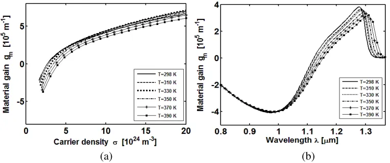
In Fig. 2(a) we report the calculated patterns of the material gaingmof the four GaInNAs-GaInAs
QWs as a function of the carrier density σ for a fixed value of the wavelength λ= 1.2888µm and for different temperature values in the range T = 298 K–390 K. We can see that, for all the values of the examined temperature range, gm assumes an increasing trend with increasing σ. For σ greater than
about 5·1024m−3the slopes of the curves decreases and the material gaingm tends to assume a constant
value (gain saturation effect). In addition, Fig. 2(b) illustrates thegm−λcurves for different temperature
values in the range T = 298 K–390 K, for a fixed value of the carrier density σ = 8·1024m−3. We can see that the curves show peaks of the material gain for wavelength valuesλp in the rangeλp= 1.28µm– 1.32µm by increasing the temperature fromT = 298 K toT = 400 K, whereas, correspondingly, thegmp
peak value decreases. The findings of Fig. 2(b) in terms of the peak of the material gain gmp and the corresponding wavelength value λp for the different temperature values in the range T = 298 K–390 K are summarized in Table 1. As expected, by increasing the temperature fromT = 298 K toT = 390 K,
Figure 1. Scheme of the ridge waveguide DNOA. The core is made of four Ga0.77In0.23N0.03As0.97 quantum wells and five Ga0.8In0.2As barrier layers.
(a) (b)
Figure 2. Calculated material gain as a function of (a) the carrier density σ for the wavelength
λ= 1.2888µm and of (b) the wavelengthλfor the carrier density σ= 8·1024m−3.
Table 1. Values of the peak of the material gaingmpand the corresponding wavelengthλpas a function
of the temperatureT for constant carrier density σ= 8·1024 m−3.
T [K] λp [µm] gmp [m−1] 298 1.2759 3.81·105 310 1.2845 3.66·105 330 1.2889 3.59·105 350 1.2932 3.46·105 370 1.3015 3.33·105 390 1.3110 3.21·105
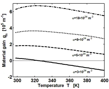
Figure 3 shows the material gain changes with temperature for the wavelength λ = 1.2888µm for four values of the carrier density σ = 3 ·1024m−3 (solid line), σ = 5·1024m−3 (dashed line),
maximum value of the material gain gmMax and, in particular, we have calculated: forσ= 5·1024m−3
gmMax = 1.82·105m−1 at temperature T = 308 K, for σ = 8·1024m−3 gmMax = 3.63·105m−1 at
T = 318 K and for σ= 18·1024m−3 gmMax= 6.72·105m−1 atT = 322 K.
The knowledge of the material gain dependence with the temperature allows for the evaluation of the influence of the temperature on the performance of the ridge waveguide 4-QW DNOA of Fig. 1 in the case of amplifier length Ltot = 130µm. The simulations have been carried out by means of the
MoL-BBPM in which the four QW active layer is accounted for by the complex value of the refractive indexna of Equation (3). Fig. 4(a) reports the gainGDNOA of the DNOA as a function of the injected current density for different values of the temperature in the range T = 298 K–390 K. Obviously, for each temperature value the gain assumes an increasing behaviour with the injected current density by passing from negative to positive values with respect to the transparency injected current densityJtr for which GDNOA = 0 dB. We can see that, by increasing the temperature from T = 298 K to T = 390 K, the curves show lower GDNOA values. In addition, by inspection of Fig. 4(b), the transparency current density Jtr increases with the temperature. In particular, by changing the temperature from 298 K to 400 K, a gain of the DNOA greater than 0 dB can be obtained for injected current values greater than
Jtr = 0.08 mA/µm2 and Jtr = 0.21 mA/µm2, respectively, thus drastically increasing the transparency
current density value.
Figure 3. Material gain gm as a function of the temperature ranging from to 298 K to 400 K for
λ= 1.2888µm for four different values of the carrier density: σ= 3·1024m−3(solid line),σ= 5·1024m−3 (dashed line), σ= 8·1024m−3 (dotted line) andσ = 18·1024m−3 (dash-dotted line).
(a) (b)
4. DILUTE NITRIDE 1-D RIDGE WAVEGUIDE PHOTONIC CRYSTAL AS ACTIVE MODULATOR
By exploiting the properties of the proposed GaInNAs-GaInAs 4-MQW ridge amplifier, we can design a novel active modulator that exhibits high performance in terms of crosstalk, contrast ratio, modulation depth and bandwidth. Fig. 5 shows the sketch of the designed photonic crystal structure patterned with an one-dimensional (1-D) grating having N = 1243 alternating ridge waveguide layers. In particular, as shown in Fig. 5, the grating unit cell is made of two ridge waveguides having different values of the ridge heightsh1 and h2, and of the ridge lengths l1 andl2. More precisely, for the first ridge waveguide we have h1 = 0.10µm and l1 = 0.12µm, whereas for the second one h2 = 1.0µm and l2 = 0.076µm, respectively. These geometrical parameters have been chosen to assure the PBG around the Bragg wavelength at λB = 1.2888µm.
A defect is introduced in the 1-D photonic crystal by changing in the central 622-th layer the corresponding ridge waveguide length from l2 to Lz and by injecting current I through the electrode placed only on the defective active region.
The switching mechanism from the OFF-state to the ON-state can be obtained by properly choosing the defect length such that the wavelength λmin of the minimum transmittance calculated without injecting current (passive case) coincides with thatλMaxof the maximum transmittance when the current is injected (active case). It is feasible because, by changing the defect length Lz, the transmittance maximum shifts within the wavelength range delimited by the two band-edges of the periodic grating evaluated without defect [15]. In addition, similar behaviour occurs in the active case by changing the value of the injected current.
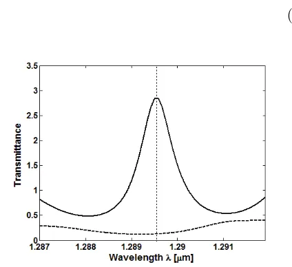
Figure 6 shows the spectra of the transmittance of the 1-D ridge waveguide grating with defect length Lz = 9.07µm in the passive case (JOF F = 0 mA/µm2, dashed curve) and in the active case
(JON = 0.496 mA/µm2, solid curve).
The transmittance T is calculated according to the following definition, both in the active and passive cases:
T = IT
IIN
(4)
Figure 5. Sketch of the proposed active switch made of a grating of N = 1243 alternating passive ridge waveguide layers having different ridge heights h1 and h2 and corresponding ridge lengths l1 and l2. The central active ridge waveguide layer having Lz length represents the
active defect introduced in the photonic crystal. The metallic electrodes are shown in black, too.
Figure 6. Spectra of the transmittance of the 1-D ridge waveguide grating with defect length Lz = 9.07µm in the passive case forJOF F = 0 mA/µm2
(dashed curve) and in the active case for JON =
0.496 mA/µm2 (solid curve). The chosen value of the defect length Lz = 9.07µm allows to
where IT is the intensity of the optical field transmitted at the output port and IIN the intensity
associated to the input signal. The intensities were calculated as:
Ii= ∫
|Ei(x)|2dx
whereEiis the electric field, and subscriptirefers to the input, transmitted, and reflected waves. Owing
to the amplification effect of the optical signal, due to the injection of current in the active region, the value of the transmittance T can be higher than unity.
A perfect coincidence of the value of the two wavelengthsλmin =λMax= 1.2896µm can be achieved at room temperatureT = 298 K for a defect lengthLz = 9.07µm and for a value of the injection current
densityJON = 0.496 mA/µm2 (ION = 9 mA). More precisely, the switching from the OFF- to the
ON-state occurs at the wavelength value λSW = 1.2896µm for which the transmittance, evaluated at the end face of the 1-D grating of Fig. 5, changes fromTOF F = 0.12 toTON = 2.84 by changing the injected current density fromJOF F = 0 mA/µm2 toJON = 0.496 mA/µm2.
The performance of the designed active modulator, can be quantified with the following figures-of-merit: the crosstalk CT = 10 Log(TOF F/TON), the modulation depth MD = 1−TOF F/TON, and the contrast ratio CR = TON/TOF F. With reference to the results of Fig. 6 we have calculated crosstalk CT =−13.6 dB, contrast ratio CR = 22.7, and modulation depth MD = 0.96 atT = 298 K. A further useful parameter is the bandwidth ∆λfor which the crosstalk is less than−12 dB around toλSW. The
calculated bandwidth value is ∆λ= 0.57 nm.
Better performance can be achieved by slightly increasing the value of the injection current density in the ON-state to JON = 0.606 mA/µm2 (ION = 11 mA). In this case the switching wavelength λSW = 1.2894µm slightly shifts towards a lower value, even though the new transmittance value TON = 3.19 increases at about 12%. Now the merit figures at temperature T = 298 K assume the
following improved values: crosstalk CT =−14.2 dB, contrast ratio CR = 26.2, modulation depth MD = 0.96, and bandwidth ∆λ= 0.67 nm.
5. MODULATOR PERFORMANCE UNDER TEMPERATURE INFLUENCE
Temperature increase strongly affects the switching characteristics. In fact, temperature primarily influences the energy bandgap and then the energy band-structure that directly impacts on the optical properties of the active layer through Fermi’s Golden rule.
(a) (b)
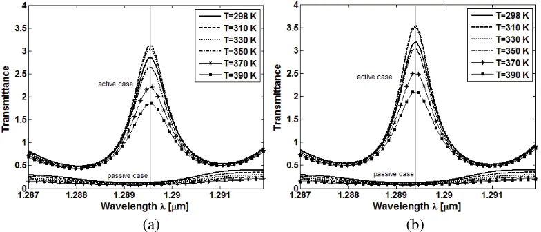
Figure 7. Spectra of the transmittance of the 1-D ridge waveguide grating in both the passive and the active cases for (a) JON = 0.496 mA/µm2 and (b) JON=0.606 mA/µm2. The minimum of the
transmittancesTOF F in the passive case coincides with the maximum of the transmittance TON in the
active case at the switching wavelength λSW = 1.2896µm (vertical solid line in Fig. 7(a)) for JON =
Figure 7 reports the spectra of the transmittance of the 1-D ridge waveguide grating with defect length Lz = 9.07µm in both the passive (JOF F = 0 mA/µm2) and the active cases (JON) for the
injection current density JON = 0.496 mA/µm2 (a) and JON = 0.606 mA/µm2 (b) for different values
of the temperature ranging from T = 298 K to T = 390 K. The coincidence of the minimum of the transmittance TOF F in the passive case with the maximum of the transmittance TON in the active
case occurs for all the temperature values at the switching wavelengthλSW = 1.2896µm (vertical solid
line in Fig. 7(a)) for JON = 0.496 mA/µm2 and at λSW = 1.2894µm (vertical solid line in Fig. 7(b))
for JON = 0.606 mA/µm2. In the active case the influence of the temperature is strongly evident. In
fact, for both the examined JON values the maximum transmittance values TON primarily increases
by increasing the temperature from T = 298 K to T = 330 K and then it decreases more and more for increasing T values. In summary, by changing the temperature from T = 298 K to T = 390 K the maximum transmittance reduces from TON = 2.84 to TON = 1.86 for JON = 0.496 mA/µm2, whereas it reduces fromTON = 3.19 toTON = 2.10 forJON = 0.606 mA/µm2.
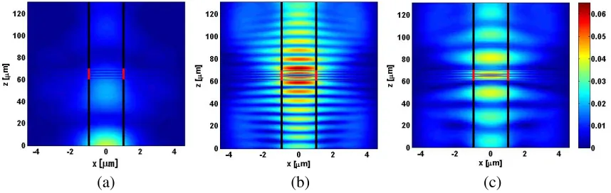
Figure 8 shows the modulus of the electric field component|E|, calculated by the BBPM-MoL along the structure at λSW = 1.2894µm, in the passive case at temperatureT = 298 K a) and in the active one ((b) and (c)) withJON = 0.606 mA/µm2for two different values of the temperature: (b)T = 298 K
and (c) T = 400 K. The defective region is marked in red. Comparing Fig. 8(a) with Figs. 8(b) and (c) we can see that in the active cases, irrespective of the temperature, a strong localization of the electromagnetic field occurs in the defective region, thus leading to a strong amplification of the signal. Moreover, it is evident that in the output sectionz= 132.072µm, the modulus of the electric field in the active cases assumes greater values with respect to that in the passive case. However, higher|E|values occur for the active case at room temperatureT = 298 K, for which we have calculated a transmittance
TON = 3.19, whereas at T = 400 K it assumes a valueTON = 1.95.
The influence of the temperature on the performances of the active dilute nitride modulator under study are evaluated with the figure-of-merit changes with the temperature. Fig. 9 shows the behaviour of crosstalk as a function of temperature for the configuration of the modulator with (a) JON = 0.496 mA/µm2 and (b) JON = 0.606 mA/µm2. For both the configurations the best crosstalk occurs for temperature T = 333 K, for which we have calculated CT = −14.8 dB for
JON = 0.496 mA/µm2 and CT = −15.5 dB for JON = 0.606 mA/µm2. We can observe that, for all the temperature values, the CT values of the modulator configuration with JON = 0.606 mA/µm2 differ at about −0.7 dB with respect to the ones with JON = 0.496 mA/µm2. In fact, it is evident
that best performances in terms of crosstalk can be obtained for the modulator configuration with
JON = 0.606 mA/µm2.
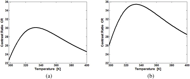
On the other hand, as shown in Fig. 10, that displays the contrast ratio as a function of the temperature for (a) JON = 0.496 mA/µm2 and (b) JON = 0.606 mA/µm2, the maximum CR value
for both the modulator configurations can be obtained for T = 333 K. The calculated maximum
(a) (b) (c)
contrast ratio is CR = 30.1 for JON = 0.496 mA/µm2 and CR = 35.4 for JON = 0.606 mA/µm2.
However, to parity of temperature the configuration with greater current density value gives the best CR performances.
Finally, Fig. 11 reports the bandwidth ∆λ for which the crosstalk is less than −12 dB around to
λSW as a function of temperature for (a) JON = 0.496 mA/µm2 and for (b) JON = 0.606 mA/µm2.
In this case, for JON = 0.496 mA/µm2 the bandwidth increases from ∆λ = 0.57 nm for T = 298 K to
∆λ= 0.82 nm for T = 360 K, and then it decreases to ∆λ= 0.81 nm for T = 400 K. On the contrary, for the modulator configuration having JON = 0.606 mA/µm2 the bandwidth assumes an increasing
trend for all the temperature values ranging from ∆λ = 0.67 nm for T = 298 K to ∆λ = 0.93 nm for
T = 400 K.
The modulation depth, for all examined cases and all temperature values assumes a constant value MD = 0.96.
(a)
(b)
Figure 9. Pattern of the crosstalk CT as a function of the temperature for injection current density in the active case (a)JON = 0.496 mA/µm2 and (b)JON = 0.606 mA/µm2. The crosstalk has a minimum
equal to CT =−14.8 dB atT = 333 K and CT =−15.5 dB atT = 333 K forJON = 0.496 mA/µm2 and JON = 0.606 mA/µm2, respectively.
(a)
(b)
Figure 10. Pattern of the contrast ratio CR as a function of the temperature for injection current density in the active case (a) JON = 0.496 mA/µm2 and (b)JON = 0.606 mA/µm2. The contrast ratio
has a maximum equal to CR = 30.1 atT = 333 K and CR = 35.4 atT = 333 K forJON = 0.496 mA/µm2
(a)
(b)
Figure 11. Pattern of the bandwidth ∆λfor CT≤ −12 dB as a function of the temperature for injection current density in the active case (a)JON = 0.496 mA/µm2 and (b) JON = 0.606 mA/µm2. In the case
ofJON = 0.496 mA/µm2 the bandwidth maximum occurs forT = 360 K for which ∆λ= 0.82 nm, while
for the JON = 0.606 mA/µm2 configuration the bandwidth assumes an increasing trend by increasing the temperature fromT = 298 K toT = 400 K.
6. CONCLUSION
The temperature performance of dilute nitride photonic devices has been analysed, particularly focusing on photonic crystal waveguide modulators. Dilute nitride multi-quantum-well PBG structures have been investigated as active ON/OFF modulators at the wavelengthλ= 1.2896µm.
The proposed devices exhibit a maximum contrast ratio equal to CR = 30.1 for injected current density JON = 0.496 mA/µm2 and CR = 35.4 for JON = 0.606 mA/µm2. The minimum crosstalk is CT = −14.8 dB for JON = 0.496 mA/µm2 and CT = −15.5 dB for JON = 0.606 mA/µm2.
Finally, the maximum bandwidth is ∆λ = 0.81 nm for JON = 0.496 mA/µm2 and ∆λ = 0.93 nm
forJON = 0.606 mA/µm2. The temperature performance of the proposed device shows a good stability
in the range T = 298 K–400 K. In particular, the CT varies of about 1.2 dB in the whole temperature range, whereas CR and ∆λ experience, respectively, a maximum variation of 25% and 30% of their maximum values. The achieved temperature stability range is comparable with the ones demonstrated, either theoretically or experimentally, in the literature for QW lasers based on dilute nitrides [9–13]. Moreover, the advantage of the proposed design, with respect to passive modulators, is to achieve an ON-OFF switching functionality together with an efficient signal amplification and a stable temperature operation.
ACKNOWLEDGMENT
The work was supported by the Photonic Interconnect Technology for Chip Multiprocessing Architectures (“PHOTONICA”) project under the Fondo per gli Investimenti della Ricerca di Base 2008 (“FIRB”) program, funded by the Italian government and by the project “Regional laboratory for synthesis and characterization of new organic and nanostructured materials for electronics, photonics, and advanced technologies” funded by the Apulia Region. The research has been conducted in the framework of the European Cooperation in Science and Technology (“COST”) Action MP0805.
APPENDIX A.
formulas:
P(AxB1−xCyD1−y) =xyP(AC) + (1−x)(1−y)P(BD) + (1−x)yP(BC) +x(1−y)P(AD) P(AxB1−xC) =xP(AC) + +(1−x)P(BC)
Material parameters used in the calculations [44] Materials
GaAs InAs InN GaN
αo (˚A) 5.6533 6.0584 4.98 4.5 αc (eV) 1.16 1.00 1.5 1.27
αv (eV) −7.17 −5.08 −1.85 −2.2 b (eV) −1.7 −1.8 −1.2 −1.7
C11 (× 1010 N/m2) 11.879 8.329 18.7 29.3
C12 (× 1010 N/m2) 5.376 4.526 12.5 15.9
γ1 6.8 20.4 1.92 2.67
γ2 1.9 8.3 0.47 0.75
γ3 2.73 9.1 0.85 1.10
Ep (eV) 28.8 21.5 25 25
where, αo: lattice constant, αc: hydrostatic deformation potential, conduction band, αv: hydrostatic
deformation potential, valence band, b: shear deformation potential, C11,12: elastic stiffness constant,
γ1,2,3: Luttinger-Kohn parameters, Ep: optical matrix parameter.
REFERENCES
1. Biberman, A. and K. Bergman, “Optical interconnection networks for high-performance computing systems,”Rep. Prog. Phys., Vol. 75, 046402, 2012.
2. Li, Z., A. Qouneh, M. Joshi, W. Zhang, X. Fu, and T. Li, “Aurora: A cross-layer solution for thermally resilient photonic network-on-chip,” Trans. Very Large Scale Integr. (VLSI) Syst., Vol. 23, No. 1, 170–183, 2015.
3. Van Campenhout, J., W. M. J. Green, and Y. A. Vlasov, “Design of a digital, ultra-broadband electro-optic switch for reconfigurable networks-on-chip,”Opt. Express, Vol. 12, 23793–23801, 2009. 4. Cal`o, G., A. D’Orazio, and V. Petruzzelli, “Broadband Mach-Zehnder switch for photonic networks
on chip,”J. Lightwave Technol., Vol. 30, No. 7, 944–952, 2012.
5. Cal`o, G. and V. Petruzzelli, “WDM performances of two- and three-waveguide Mach-Zehnder switches assembled into 4×4 matrix router,”Progress In Electromagnetics Research Letters, Vol. 38, 1–16, 2013.
6. Padmaraju, K. and K. Bergman, “Resolving the thermal challenges for silicon microring resonator devices,” Nanophotonics, Vol. 3, 269–281, 2014.
7. Kondow, M., T. Kitatani, S. Nakatsuka, M. C. Larson, K. Nakahara, Y. Yazawa, M. Okar, and K. Uomi, “GaInNAs: A novel material for long wavelength semiconductor lasers,” IEEE J. Sel. Top. Quantum Electron, 719–730, 1997.
8. Konttinen, J., P. Tuomisto, M. Guina, and M. Pessa, “Recent progress in development of GaInNAs-based photonic devices,”Proc. IEEE ICTON 2006, 189–192, 2006.
9. Dumitrescu, M., A. Larsson, Y. Wei, E. Larkins, P. Uusimaa, K. Schulz, and M. Pessal, “High-performance 1.3µm dilute-nitride edge-emitting lasers,”International Semiconductor Conference, 2007. CAS 2007, Sinaia, Romania, Oct. 15–17, 2007.
modulated GaInNAs-GaAs 1.35-µm laser for metropolitan applications,”IEEE Photonics Technol. Lett., Vol. 17, No. 5, 971–973, 2005.
11. Gustavsson, J. S., Y. Q. Wei, M. Sadeghi, S. M. Wang, and A. Larsson, “10 Gbit/s modulation of 1.3µm GaInNAs lasers up to 110◦C,”Electron. Lett., Vol. 42, No. 16, 925–926, 2006.
12. Wei, Y. Q., J. S. Gustavsson, M. Sadeghi, S. M. Wang, A. Larsson, P. Savolainen, P. Melanen, and P. Sipil¨a, “Uncooled 2.5 Gb/s operation of 1.3µm GaInNAs DQW lasers over a wide temperature range,”Opt. Express, Vol. 14, 2753–2759, 2006.
13. Kima, C. K. and Y. H. Lee, “Thermal characteristics of optical gain for GaInNAs quantum wells at 1.3µm,”Appl. Phys. Lett., Vol. 79, No. 19, 3038–3040, 2001.
14. Alexandropoulos, D., M. J. Adams, Z. Hatzopoulos, and D. Syvridis, “Proposed scheme for polarization insensitive GaInNAs-based semiconductor optical amplifiers,” IEEE J. Quantum Electron., Vol. 41, 817–822, 2005.
15. Cal`o, G., D. Alexandropoulos, A. D’Orazio, and V. Petruzzelli, “Wavelength selective switching in dilute nitrides multi quantum well photonic band gap waveguides,”Phys. Status Solidi B-Basic Solid State Phys., Vol. 248, No. 5, 212–215, 2011.
16. Schires, K., R. Al Seyab, A. Hurtado, V.-M. Korpijarvi, M. Guina, I. D. Henning, and M. J. Adams, “Optically-pumped dilute nitride spin-VCSEL,” Opt. Express, Vol. 20, No. 4, 3550–3555, 2012. 17. Bonnefont, B., M. Messant, O. Boutillier, F. Gauthier-Lafaye, A. Lozes-Dupuy, M. V. Sallet,
K. Merghem, L. Ferlazzo, J. C. Harmand, A. Ramdane, J. G. Provost, B. Dagens, J. Landreau, O. Le Gouezigou, and X. Marie, “Optimization and characterization of InGaAsN/GaAs quantum-well ridge laser diodes for high frequency operation,” Opt. Quantum Electron., Vol. 38, No. 4–6, 313–324, 2006.
18. Korpijarvi, V.-M., T. Leinonen, J. Puustinen, Harkonen, and M. D. Guina, “11 W single gain-chip dilute nitride disk laser emitting around 1180 nm,” Opt. Express, Vol. 18, No. 25, 25633–25641, 2010.
19. Joannopoulos, J. D., R. D. Meade, and J. N. Winn,Photonic Crystals: Molding the Flow of Light, 2nd Edition, Princeton Univ. Press, Princeton, NJ, 2008.
20. Cal`o, G., A. Farinola, and V. Petruzzelli, “Equalization in photonic bandgap multiwavelength filters by the Newton binomial distribution,” J. Opt. Soc. Amer. B, Vol. 28, No. 7, 1668–1679, Jul. 2011.
21. Cal`o, G. and V. Petruzzelli, “Compact design of photonic crystal ring resonator 2×2 routers as building blocks for photonic networks on chip,”J. Opt. Soc. Am. B, Vol. 31, No. 3, 517–525, 2014. 22. Cal`o, G. and V. Petruzzelli, “Wavelength routers for optical networks on chip using optimized
photonic crystal ring resonators,”IEEE Photonics J., Vol. 5, No. 3, 7901011, 2013.
23. Cal`o, G., A. D’Orazio, M. De Sario, L. Mescia, V. Petruzzelli, and F. Prudenzano, “Tunability of photonic band gap notch filters,”IEEE Trans. Nanotechnol., Vol. 7, 273–284, 2008.
24. Cowan, A. R. and J. F. Young, “Mode Matching for second-harmonic generation in photonic crystal waveguides,”Phys. Rev. B, Vol. 65, 085106, 2002.
25. Bendickson, J. M., J. P. Dowling, and M. Scalora, “Analytic expressions for the electromagnetic mode density in finite, one-dimensional, photonic band-gap structures,” Phys. Rev. E, Vol. 53, 4107–4121, 1996.
26. Cal`o, G., V. Petruzzelli, L. Mescia, and F. Prudenzano, “Study of gain in photonic band gap active InP waveguides,”J.Opt. Soc. Amer. B, Vol. 26, No. 12, 2414–2422, Dec. 2009.
27. Cal`o, G., M. Grande, D. Alexandropoulos, and V. Petruzzelli, “Photonic band gap active waveguide filters based on diluite nitrides,” Phys. Status Solidi C, Vol. 10, No. 4, 567–572, 2013.
28. Cal`o, G., D. Alexandropoulos, and V. Petruzzelli, “Active WDM filter on dilute nitride quantum well photonic band gap waveguide,”Progress In Electromagnetics Research Letters, Vol. 35, 37–49, 2012.
30. Chang C. and S. L. Chuang, “Modelling of strained quantum-well lasers with spin-orbit coupling,”
IEEE. J. Select. Top. Quantum. Electron., Vol. 1, 218–229, 1995.
31. Chao, C. Y. and S. L. Chuang, “Spin-orbit-coupling effects on the valence-band structure of strained semiconductor quantum wells,” Phys. Rev. B, Vol. 46, 4110–4122, 1992.
32. Chuang, S. L., “Efficient band-structure calculations of strained quantum wells using a two by two Hamiltonian,” Phys. Rev. B., Vol. 43, 9649–9661, 1991.
33. Chuang, S. L., Physics of Optolectronic Devices, Wiley Interscience, New York, 1995.
34. Kima, C. K. and Y. H. Lee, “Thermal characteristics of optical gain for GaInNAs quantum wells at 1.3µm,”Appl. Phys. Lett. Vol. 79, No. 19, 3038–3040, 2001.
35. Pregla, R., “MOL-BPM method of lines based beam propagation method,” Progress In Electromagnetics Research, Vol. 11, 51–102, 1995.
36. Gerdes, J., “Bidirectional eigenmode propagation analysis of optical waveguides based on method of lines,” Electron. Lett., Vol. 30, 550–551, 1994.
37. D’Orazio, A., M. De Sario, V. Petruzzelli, and F. Prudenzano, “Bidirectional beam propagation method based on the method of lines for the analysis of photonic band gap structures,” Opt. Quantum Electron., Vol. 35, 629–640, 2003.
38. Cal`o, G., A. D’Orazio, M. Grande, V. Marrocco, and V. Petruzzelli, “Active InGaAsP/InP photonic bandgap waveguides for wavelength-selective switching,”IEEE J. Quantum Electron., Vol. 47, 172– 181, 2011.
39. Buus, J., “The effective index method and its application to semiconductor laser,”IEEE J. Quant. Elect., Vol. 18, 1083–1089, 1982.
40. Makino, T., “Effective index matrix analysis of distributed feedback semiconductor lasers,” IEEE J. Quant. Elect., Vol. 28, 434–440, 1982.
41. Working Group I, COST 216, “Comparison of different modeling techniques for longitudinally invariant integrated optical waveguides,”IEEE Proceedings, Vol. 136, No. 5, 273–280, Oct. 1989. 42. Batrak, D. V. and S. A. Plisyuk, “Applicability of the effective index method for simulating ridge
optical waveguides,”Quantum Electron., Vol. 36, 349–352, 2006.
43. Alexandropoulos, D., M. J. Adams, Z. Hatzopoulos, and D. Syvridis, “Proposed scheme for polarization insensitive GaInNAs-based semiconductor optical amplifiers,” IEEE J. Quantum Electron., Vol. 41, 817–822, 2005.