Available online: https://edupediapublications.org/journals/index.php/IJR/ P a g e | 3737
A Novel High Performance Sense Amplifier based Low
Power SRAM Memory cell
Vishani P Sheth & Dr. Towheed Sultana
1PG Scholar, Dept. of VLSI-SD, J B Institute of Engineering & Technology (Autonomous), Telangana, India.
2Principal, Dept. of ECE, J B Institute of Engineering & Technology (Autonomous), Telangana, India.
Abstract:
Reduced energy potency has invariably been the foremost aim of the custom and automatic digital circuit techniques. Though increasing nano-devices area unit expected to exchange the prevailing MOSFET devices, aloof from being as mature as semiconductor devices and their full potential and promise are a few years faraway from being sensible. The analysis represented during this exposition consists of 4 main components. it's a
replacement circuitdesign of a difference limen
logic flip- flop known as n-NOR. The NNOR gate may be an edge-triggered multi-input serial cell whose next state perform is a function of its inputs. a replacement approach, known as hybridisation, that replaces flip flops and components of their logic comes with n-NOR cells is represented. The ensuing hybrid circuit, that consists of standard logic cells and n-NORs, is shown to own considerably less power consumption, smaller space, less standby power and fewer power variation.It is a replacement design of a field programmable array, known as field programmable threshold logic array (FPTLA), during which the quality operation table (LUT) is replaced by a NNOR is represented. The FPTLA is shown to own the maximum amount as eightieth lower energy delay
product compared to traditional FPGA
exploitation well- better-known FPGA
modeling tool known as VPR. it's a unique clock skewing technique that creates use of the completion detection feature of the differential mode flip- flops is represented. This clock skewing methodology improves the world and power of the ASIC circuits by increasing slack on temporal order ways.
Keywords: NAND cell , Memory, TG Gate
I.Introduction
:Available online: https://edupediapublications.org/journals/index.php/IJR/ P a g e | 3738
techniques for reducing power at the logic logic gate levels are completely explored, going away minor chance for improvement power potency.
Accordingly, the main target has shifted to the very best levels of style, together with power economical micro-architectures, memory, compilers, and OS, and system level management, together with thermal-aware dynamic frequency and voltage management, thread migration among processor cores. One a part of digital CMOS circuits that has not modified is however logic functions ar computed. However, there exists a correct set of uniting Boolean functions, referred to as threshold functions, which may be basically computed by totally different mechanisms, that presents the chance of more enhancements in power consumption, performance, and area, that has not been sufficiently explored. Let X =(x1, x2, . . . ,Xn), xi ∈ , W=(w1,w2, . . . ,on), wi∈ R, and T ∈ R. A unit Boolean operate f (X) is termed a mathematical function if there exist weights w and a set threshold T, the rationale for examining threshold gates as logic primitives stems from the very fact that they're computationally a lot of powerful than the quality AND/OR logic primitives. abundant common logic functions, like then n-bit parity, n-bit multiplication, division, powering, sorting and might be computed by polynomial size threshold networks of a set one among the numbers of levels, whereas constant would need exponential size AND/ORnetworks. the quality of threshold networks and constructive strategies for varied sorts of arithmetic functions, together with size-depth and weight depth tradeoffs.As results recommend that the brink gates and networks will doubtless result
in important reductions in circuit space, power, and delay.
2. Threshold gate:
The design for a logic element that employs differential logic, named as a pNAND cell, Is represented. like alternative implementations within the same class, a pNAND cell is clocked, and its behavior will beabstracted to be that of a multi-input edge-triggered flipflop (ETFF). Whereas a traditional D-type ETFF (D-FF) computes the establish perform f (x) = x on a clock edge, apNAND cell computes a function f (x1, x2, . . . ,xn) on a clock edge. what is more, just like the D-FF, a pNAND cell will be created scannable and produce other options, like asynchronous predetermined and clear.
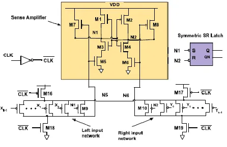
Fig:1 NAND cell
Cell Operation:
Available online: https://edupediapublications.org/journals/index.php/IJR/ P a g e | 3739
1) 2 teams of parallel pFET transistors said because the left input network (LIN) and also the right input network (RIN);
2) a way electronic equipment (SA), that consists of a try of cross-coupled NAND gates; and
3) a set–reset (SR) latch. The cell is operated in 2 phases: reset (CLK = zero) and analysis (CLK 0 → 1). For the instant, ignore the transistors M9 and M10 within the carver and also the RIN.
1) Reset Phase:
With CLK = zero, the 2 discharge devices M18 and M19 pull nodes N5 and N6 low, that close up M5 and M6, disconnecting all methods from N1 and N2 to ground. additionally, M7 and M8 ar active, which ends in N1 and N2 being force high. The nFETsM3 and M4 ar ON. With N1 and N2 being high, the state of the SR latch doesn't amendment.
2) Evaluation Phase:
This corresponds to once CLK zero → one. associate input that leads to nine active devices within the architect and r active devices within the RIN . The signal assignment procedure can make sure that nine _= r . Assume that nine >r . As a result, the electrical phenomenon of the architect is on top of that of the RIN. because the discharge devices M18 and M19 square measure turned OFF, each N5
and N6 can rise to one. attributable to the upper conduction of the architect, node N5 can begin to rise 1st, that activates M5. With M3 = one, N1 can begin to discharge through M3 and M5. The delay within the begin time for charging N6 attributable to the lower electrical phenomenon of the RIN permits for N1 to show ON money supply and switch OFF M4. Thus, though N2 starts to discharge, its any discharge is obstructed as money supply activates, leading to N2 obtaining force back to one. As a result, the output node N1 is zero and N2 is one. because the circuit and its operation square measure rhombohedral, if _.
Implementation:
Available online: https://edupediapublications.org/journals/index.php/IJR/ P a g e | 3740
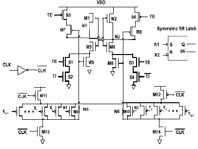
cell. though there exist many ways that to implement scan for a PNAND cell, the one shown in Figure one.2 has negligible impact on the cell's performance and strength throughout traditional operation. All alternative variations were considerably worse during this regard. the extra transistors for scan square measure labelled as S1 through S6. within the traditional mode, the signals TE (test enable) and TI (test input) square measure each zero, that disables the scan connected transistors (S1 through S4), and reduces the circuit perform to the one shown in Figure one.2. within the scan mode, the TE signal itself acts as a clock for a PNAND. in truth regular clock CLK should be command zero for the scanning mechanism to figure. Therefore, if a circuit includes a mixture of D-FFs and PNAND cells, the PNAND cells should be a part of a separate scan chain. a standard TE signal is employed for each the scan chains. but the method this TE signal is operated is totally different from the traditional scanning mechanism. 1st the signal TE is command high and knowledge is scanned into regular flipflops (conventional way). Once this can be finished, the CLK is command zero and following procedure is performed to keep knowledge bits in PNANDs. Signal GTI (global check input) is that the entry purpose for the
scan knowledge input to the PNAND chain.
Once this is often finished, the CLK is control zero and following procedure is performed to hold on knowledge bits in PNANDs. Signal GTI (global check input) is that the entry purpose for the scan knowledge input to the PNAND chain.
1. Set CLK = zero and TE = zero.
2. Set GTI = i'th little bit of the input (i = zero initially).
3. Set TE = 1. every PNAND registers its TI input.
4. Set TE = 0.
5. Increment i and repeat till the top of stream. Note that as long as CLK = zero, the toggling of TE signal alone doesn't alter the info already hold on within the standard D-Flipflop scan chain.
4. Sense amplifier based flip-flops:
Available online: https://edupediapublications.org/journals/index.php/IJR/ P a g e | 3741
compose the electronic equipment on a semiconductor chip (integrated circuit); the term itself dates back to the age of core memory. sense electronic equipment is a component of the scan electronic equipment that's used once information is scan from the memory; its role is to sense the low power signals from alittle line that represents an information bit (1 or 0) keep in an exceedingly memory cell, and amplify the little voltage swing to recognizable logic levels therefore the information may be taken properly by logic outside the memory. trendy sense-amplifier circuits encompass 2 to 6 (usually four) transistors, whereas early sense amplifiers for core memory generally contained as several as thirteen transistors
Result analysis:
Fig:2Threshold pNAND cell
Fig:3 Waveform for Threshold pNAND cell
Available online: https://edupediapublications.org/journals/index.php/IJR/ P a g e | 3742
Table1: Comparision Parameters
Conclusion:
In this paper, we tend to delineate a replacement, machine-driven methodology for the planning of digital ASIC circuits employing a combination of standard logic gates and threshold logic flip-flops. The methodology delineate during this paper was exercised on variety of complicated perform blocks, and important enhancements in dynamic power, leakage, area, and power variation were incontestible. The demonstrations were supported full, layout extracted internet lists.
References:
[1] P. R. Panda, A. Shrivastava, B. V. N. Silpa, and K. Gummidipudi, Power- Efficient System Design. New York, NY, USA: Springer, 2010. [2] K.-Y. Siu, V. Roychowdhury, and T. Kailath, Discrete Neural Computation: A
Theoretical Foundation. Englewood Cliffs, NJ, USA: Prentice-Hall, 1995.
[3] V. Beiu, ―A survey of perceptron circuit complexity results,‖ in Proc. Int. Joint Conf. Neural Netw. (IJCNN), Jul. 2003, pp. 989–994. [4] V. Beiu, J. M. Quintana, and M. J. Avedillo, ―VLSI implementations of threshold logic—A comprehensive survey,‖ IEEE Trans. Neural Netw., vol. 14, no. 5, pp. 1217–1243, Sep. 2003.
[5] B. Nikoli´c, V. G. Oklobdžija, V. Stojanovi´c, W. Jia, J. K.-S. Chiu, and M. M.-T. Leung, ―Improved sense-amplifier- based flip-flop: Design and measurements,‖ IEEE J. Solid-State Circuits, vol. 35, no. 6, pp. 876– 884, Jun. 2000.
[6] R. Strandberg and J. Yuan, ―Single input current-sensing differential logic (SCSDL),‖ in Proc. IEEE Int. Symp.Circuits Syst., vol. 1. May 2000, pp. 764–767.
[7] M. Padure, S. Cotofana, and S. Vassiliadis, ―Design and experimental results of a CMOS flip-flop featuring embedded threshold logic,‖ in Proc. Int. Symp. Circuits Syst., May 2003, pp.
V-253–V- 256.
Available online: https://edupediapublications.org/journals/index.php/IJR/ P a g e | 3743
family for DSM technology,‖ in Proc. IEEE Int. Conf. Microelectron., Dec. 2010, pp. 52–55. [9] S. Leshner, ―Modeling and implementation of threshold logic circuits and architectures,‖ Ph.D. dissertation, Comput.Sci., Arizona State Univ., Tempe, AZ, USA, 2010.
[10] V. J. Modiano, ―Majority logic circuit using a constant current bias,‖ U.S. Patent 3 155 839, Nov. 3, 1964.
[11] R. Z. Fowler and E. W. Seymour, ―Direct coupled, current mode logic,‖U.S. Patent 3 321 639, May 23, 1967.
[12] J. A. Hidalgo-López, J. C. Tejero, J. Fernández, and A. Gago, ―New types of digital comparators,‖ in Proc. IEEE Int. Symp. Circuits Syst., Apr./May 1995, pp. 29–32.
[13] J. M. Quintana, M. J. Avedillo, R. Jiménez, and E. Rodríguez-Villegas, ―Practical low-cost CPL implementations threshold logic functions,‖ in Proc. 11th Great Lakes Symp. VLSI, 2001,
pp. 139–144.