DESIGN AND IMPLEMENTATION OF EFFICIENT
HIGH SPEED VEDIC MULTIPLIER USING
REVERSIBLE GATES
Boddu Suresh
1,
B.Venkateswara Reddy
2 1PG Scholar,
2Associate Professor, HOD, Dept of ECE
Vikas College of Engineering &Technology, Nunna, A.P, (India)
ABSTRACT
The main aim of the project is to improve the speed of the complex multiplier by using Vedic mathematics.
This 'Vedic Mathematics' is the name given to the ancient system of mathematics, or, to be precise, a unique
technique of calculations based on simple rules and principles, with which any mathematical problem can
done with the help of arithmetic, algebra, geometry or trigonometry can be solved. Traditionally complex
multiplier provides less speed only, because it does not use Vedic Mathematics concept. Reversible
computation is an emerging area of research, having applications in nanotechnology, low power designand
quantum computing. It is proved that reversible logic has zero internal power dissipation. Multiplication
plays an important role in the processors. It is one of the basic arithmetic operations and it requires more
hardware resources and processing time than the other arithmetic operations. Vedic mathematic is the
ancient Indian system of mathematic. It has a unique technique of calculations based on 16 Sutras. The
multiplication sutra between these 16 sutras is the Urdhva Tiryakbhyam sutra which means vertical and
crosswise. In this paper it is used for designing a low latency and reduced resources 4*4 and 8*8 Vedic
multiplier. The proposed system is design using Verilog HDL and is implemented through Xilinx ISE 14.2.
Navigator and modelsim10.01 soft ware.
Keywords: Vedic Multiplier, Urdhva Tiryakbhayam Sutra, Reversible Logic, Xilinx ISE 14.2,
modelsim10.01
I. INTRODUCTION
Multiplication is one of the more silicon-intensive functions, especially when implemented in Programmable
Logic. Multipliers are key components of many high performance systems such as FIR filters, Microprocessors,
Digital Signal Processors, etc. A system's performance is generally determined by the performance of the
multiplier, because the multiplier is generally the slowest element in the system. Furthermore, it is generally the
most area consuming. Hence, optimizing the speed and area of the multiplier is a major design issue. Vedic
mathematics is the ancient Indian system of mathematics which mainly deals with Vedic mathematical formulae
which means the store-house of all knowledge. Vedic mathematics was reconstructed from the ancient Indian
scriptures (Vedas) by Sri Bharati Krisna Tirthaji (1884-1960), after his eight years of research on Vedas
.According to his research, Vedic mathematics is mainly based on sixteen principles or word-formulae which
are termed as Sutras.
This paper is an extension of the previous work which tries to optimize the circuit proposed in the paper is
organized as follows: The section II gives the basics of reversible logic along with the literature review.
Section III explains the Urdhva Tiryakbhayam algorithm. The section IV describes the modifications of the
previous design in order to evolve the optimized design. Section V compares the proposed design with the
other non Vedic multipliers as well as the previous Vedic multiplier design and draws a conclusion claiming
the versatility of Reversible Urdhva Tiryakbhayam multiplier.
II. REVERSIBLE LOGIC
2.1 Literature Survey and Significance of reversible logic
Most of the gates used in digital design are not reversible for example NAND, OR and EXOR gates. A
Reversible circuit/gate can generate unique output vector from each input vector, and vice versa, i.e., there is
a one to one correspondence between the input and output vectors. Thus, the number of outputs in a
reversible gate or circuit has the same as the number of inputs, and commonly used traditional NOT gate is
the only reversible gate. Each Reversible gate has a cost associated with it called Quantum cost. The
Quantum cost of a Reversible gate is the number of 2*2 Reversible gates or Quantum logic gates required in
designing. One of the most important features of a Reversible gate is its garbage output i.e., every input of
the gate which is not used as input to other gate or as a primary output is called garbage output. In digital
design energy loss is considered as an important performance parameter. Part of the energy dissipation is
related to non-ideality of switches and materials. Higher levels of integration and new fabrication processes
have dramatically reduced the heat loss over the last decades. The power dissipation in a circuit can be
reduced by the use of Reversible logic. Landauer’s principle states that irreversible computations generates
heat of (KTln2) for every bit of information lost, where K is Boltzmann’s constant and T the absolute
temperature at which the computation performed. Bennett showed that if a computation is carried out in
Reversible logic zero energy dissipation is possible, as the amount of energy dissipated in a system is directly
related to the number of bits erased during computation. The design that does not result in information loss is
irreversible. A set of reversible gates are needed to design reversible circuit. Several such gates are proposed
over the past decades. Arithmetic circuits such as Adders, Subtractors, Multipliers and Dividers are the
essential blocks of a Computing system.
2.2 Some of Reversible Logic Gates
There exist many reversible gates in the literature. Among them 2*2 Feynman gate, 3*3 Fredkin gate, 3*3
Toffoli and 3*3 Peres is the most referred. The detailed cost of a reversible gate depends on any particular
realization of quantum logic. Generally, the cost is calculated as a total sum of 2*2 quantum primitives used.
realization of a complete (universal) 3*3 reversible gate is Peres gate and its cost is 4.
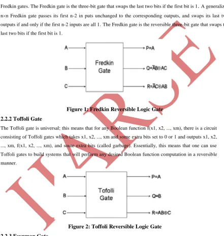
2.2.1 Fredkin Gate
The Fredkin gate (also CSWAP gate) is a computational circuit suitable for reversible computing, invented by
Ed Fredkin. It is universal, which means that any logical or arithmetic operation can be constructed entirely of
Fredkin gates. The Fredkin gate is the three-bit gate that swaps the last two bits if the first bit is 1
.
A generalizedn×n Fredkin gate passes its first n-2 in puts unchanged to the corresponding outputs, and swaps its last two
outputs if and only if the first n-2 inputs are all 1.The Fredkin gate is the reversible three-bit gate that swaps the
last two bits if the first bit is 1.
Figure 1: Fredkin Reversible Logic Gate
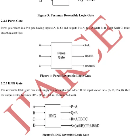
2.2.2 Toffoli Gate
The Toffoli gate is universal; this means that for any Boolean function f(x1, x2, ..., xm), there is a circuit
consisting of Toffoli gates which takes x1, x2, ..., xm and some extra bits set to 0 or 1 and outputs x1, x2,
..., xm, f(x1, x2, ..., xm), and some extra bits (called garbage). Essentially, this means that one can use
Toffoli gates to build systems that will perform any desired Boolean function computation in a reversible
manner.
Figure 2: Toffoli Reversible Logic Gate
2.2.3 Feynman Gate
The Feynman gate which is a 2*2 gate and is also called as Controlled NOT and it is widely used for fan-out
Figure 3: Feynman Reversible Logic Gate
2.2.4 Peres Gate
Peres gate which is a 3*3 gate having inputs (A, B, C) and outputs P = A; Q = A XOR B; R = AB XOR C. It has
Quantum cost four.
Figure 4: Peres Reversible Logic Gate
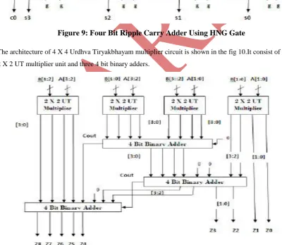
2.2.5 HNG Gate
The reversible HNG gate can work singly as a reversible full adder. If the input vector IV = (A, B, Cin, 0), then
the output vector becomes OV = (P=A, Q=Cin, R=Sum, S=Cout).
Figure 5: HNG Reversible Logic Gate
III. URDHVA TIRYAKBHAYAM
MULTIPLICATION ALGORITHM
Urdhva Tiryakbhayam (UT) is a multiplier based on Vedic mathematical algorithms devised by ancient
Indian Vedic mathematicians. Urdhva Tiryakbhayam sutra can be applied to all cases of multiplications viz.
Binary, Hex and also Decimals. It is based on the concept that generation of all partial products can be done
products and their summation is obtained using Urdhva Tiryakbhayam. Unlike other multipliers with the
increase in the number of bits of multiplicand and/or multiplier the time delay in computation of the product
does not increase proportionately. Because of this fact the time of computation is independent of clock
frequency of the processor. Hence one can limit the clock frequency to a lower value. Also, since processors
using lower clock frequency dissipate lower energy, it is economical in terms of power factor to use low
frequency processors employing fast algorithms like the above mentioned. The Multiplier based on this sutra
has the advantage that as the number of bits increases, gate delay and area increases at a slow pace as
compared to other conventional multipliers.
Algorithm:Multiplication of 101 by 110
1. We will take the right-hand digits and multiply them together. This will give us LSB digit of the answer.
2. Multiply LSB digit of the top number by the second bit of the bottom number and the LSB of the bottom
number by the second bit of the top number. Once we have those values, add them together.
3. Multiply the LSB digit of bottom number with the MSB digit of the top one, LSB digit of top number
with the MSB digit of bottom and then multiply the second bit of both, and then add them all together.
4. This step is similar to the second step, just move one place to the left. We will multiply the second digit
of one number by the MSB of the other number.
Finally, simply multiply the LSB of both numbers together to get the final product.
IV. OPTIMIZATION OF THE URDHVA
TIRYAKBHAYAM MULTIPLIER
The conventional logic design implementation of a 2x2 Urdhva Tiryakbhayam multiplier using the irreversible
logic gates is a shown in the Figure 7 In the four expressions for the output bits are derived from this figure and
are used to obtain the reversible implementation as shown in Figure 8 The circuit uses five Peres gates and one
Feynman gate. This design has a total quantum cost of 21, number of garbage outputs as 11 and number of
constant inputs 4. The gate count is 6. This design does not take into consideration the fan outs. The overall
performance of the UT multiplier is scaled up by optimizing each individual unit in terms of quantum cost,
garbage outputs etc
Figure 7: Conventional 2x2 Urdhva Tiryakbhayam Multiplier
.The 2 X 2 Urdhva Tiryakbhayam multiplier using conventional logic will have 4 outputs. The logical
expressions are given below
q0= a0.b0
ql= (a1.b0) xor (a0.bl)
q2= (a0.al.b0.bl) xor (al.bl)
q3= a0.al.b0.bl
The reversible logic implementation of the above expressions requires four peres gate and one Feynman
(CNOT) gate. The reversible logic implementation of 2 X 2 UT multiplier is shown in the Fig 8 The quantum
cost of the 2X2 Urdhva Tiryakbhayam Multiplier is found to be 21. The number of garbage outputs is 9 and
number of constant inputs is 4.
The partial products generated using the 2 X 2 UT multiplier are need to be added using the four bit adder. The
four bit ripple carry adder unit was designed using the HNG reversible gate. The four bit ripple carry adder unit
using HNG gate is shown in the Fig 9.
The quantum cost of 4 bit adder unit using HNG gate is 24. The number of garbage output is 8 and constant
Input is 4.
Figure 9: Four Bit Ripple Carry Adder Using HNG Gate
The architecture of 4 X 4 Urdhva Tiryakbhayam multiplier circuit is shown in the fig 10.It consist of four
2 X 2 UT multiplier unit and three 4 bit binary adders.
The architecture of 8 X 8 Urdhva Tiryakbhayam multiplier circuit is shown in the fig 11.It consist of four
4 X 4 UT multiplier unit and three 8 bit binary adders.
Figure 11: AN 8X8 UT Multiplier Using Reversible Logic Gate.
We have designed the 4 x 4, 8 x 8 UT multipliers in Verilog HDL They are proposed adders which are better
than Array adder.
V. RESULTS
The following figures 12 to 5.8 show the graphical representation of Top View, RTL schematic and wave form
representation. The design of the reversible 2x2, 4x4 and 8x8 multipliers is logically verified using XILINX
14.2i.And modelsim the design is also implemented using Spartan 3E environment.
5.1 Top View
Figure 12
Figure 13
Figure 12: Top View of 4 X 4 UT Multiplier Using Reversible Logic Gates
5.2 RTL Schematic
Figure 14: RTL Schematic of 4 X 4 UT Multiplier Using Reversible Logic Gates
Figure 15: RTL Schematic of 8 X 8 UT Multiplier Using Reversible Logic Gates
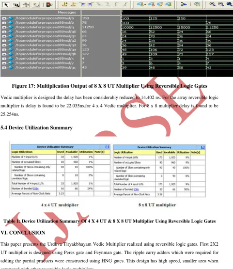
5.3 Multiplication Output
Figure 17: Multiplication Output of 8 X 8 UT Multiplier Using Reversible Logic Gates
Vedic multiplier is designed the delay has been considerably reduced to 14.402 ns. For the array reversible logic
multiplier is delay is found to be 22.035ns.for 4 x 4 Vedic multiplier. For 8 x 8 multiplier delay is found to be
25.254ns.
5.4 Device Utilization Summary
Table 1: Device Utilization Summary Of 4 X 4 UT & 8 X 8 UT Multiplier Using Reversible Logic Gates
VI. CONCLUSION
This paper presents the Urdhva Tiryakbhayam Vedic Multiplier realized using reversible logic gates. First 2X2
UT multiplier is designed using Peres gate and Feynman gate. The ripple carry adders which were required for
adding the partial products were constructed using HNG gates. This design has high speed, smaller area when
compared with other reversible logic multipliers.
REFERENCES
[1] Swami Bharati Krsna Tirtha, Vedic Mathematics. Delhi: Motilal Banarsidass publishers 1965
[2] Rakshith Saligram and Rakshith T.R. "Design of Reversible Multipliers for linear filtering Applications in
[3] R. Landauer,"Irreversibility and Heat Generation in the Computational Process", IBM Journal of Research
and Development, 5, pp.183-191, 1961.
[4] H. Thapliyal and M.B. Srinivas, "Novel Reversible Multiplier Architecture Using Reversible TSG Gate",
Proc. IEEE International Conference on Computer Systems and Applications, pp. 100-103, March 20 06.
[5] Shams, M., M. Haghparast and K. Navi, Novel reversible multiplier circuit in nanotechnology. World Appl.
Sci. J.,3(5): 806-810.
[6] Somayeh Babazadeh and Majid Haghparast, "Design of a Nanometric Fault Tolerant Reversible Multiplier
Circuit" Journal of Basic and Applied Scientific Research, 2012.
[7] H. Thapliyal and M.B. Srinivas, "Reversible Multiplier Architecture Using TSG Gate", Proc. IEEE
International Conference on Computer Systems and Applications, pp. 241- 244, March 20 07.
[8] M. Haghparast et al. , "Design of a Novel Reversible Multiplier Circuit using HNG Gate in
Nanotechnology," in World Applied Science Journal, Vol. 3, No. 6, pp. 974-978, 2008.
[9] M. S. Islam et al. , "Realization of Reversible Multiplier Circuit," in Information Tech. 1, Vol. 8, No. 2, pp.
117-121, 2005.
[10] M S Islam, M M Rahman, Z Begum and M Z Hafiz, 2009. Low Cost Quantum Realization of Reversible
Multiplier Circuit. Information Technology Journal, vol. 8(2), pp. 208-213.
[11] A. Peres, Reversible logic and quantum computers, Phys. Rev. A 32 (1985) 3266-3276.
[12] Rakshith Saligram and Rakshith T.R. "Novel Code Converter Employing Reversible Logic", International
Journal of Computer Applications (IJCA), August 2012. 781
[13] G Ganesh Kumarand V Charishma, Design of high speed vedic multiplier using vedic mathematics