^ . vj^;
f
A Digital Signal Processing Solution for
Multichannel Base Stations
by
Scott Leyonhjelm, B.Eng (Hons.)
A thesis submitted for the degree of
Doctor of Philosophy
at
Victoria University of Technology
November, 1995.
Department of Electrical and Electronic Engineering, PO BOX 14428, MCMC, 8001,
30001005034048
Leyonhjelm, Scott
Radio communication systems of the future will require a large increase in user capacity. To achieve this, cell sizes will reduce and the number of base stations will increase. Current base station architectures use analogue combining techniques which are expensive, voluminous and inflexible. This thesis investigates a Digital Signal Processing (DSP) solution which produces a cheaper, smaller and more flexible multichannel base station transmitter design. The main design challenges of the new DSP low power combining architecture are the multichannel combining algorithm, the frequency translation of the multichannel signal to radio frequency, the Digital to Analogue Conversion (DAC) interface and the wideband ultra-linear power amplifier. This thesis considers the pre-power amplifier stages.
Combining the channels in a digital signal processing environment provides considerable flexibility, but the computational requirements are very high. The minimisation of computational load is achieved by combining the channels at baseband with efficient algorithms.
Four upconversion techniques, currentiy used in single channel applications, are investigated for use in a wideband multichannel environment. Comparisons reveal that analogue direct upconversion currently provides the most attractive solution because a lower performance DAC is required and less computation is needed. However, amplitude and phase mismatch between the In Phase and Quadrature circuits cause undesired sideband responses that exceed radio system specifications. A novel adaptive compensation method leads to an improved performance and a lower computational overhead compared to previous techniques.
This thesis describes the development of a low power combining digital signal processing architecture for future radio base station transmitters. The goal of the project is to produce a base station that is small, cheap and greatly more flexible than the conventional base station design.
The idea for the low power combining architecture was described in the 1980's and its advantages over the conventional design have since been well recognised. However, four technological challenges have impeded the immediate development of the digital signal processing low power combining technique:
• the large amount of computation required to combine multiple channels in a digital signal processor,
• the high degree of linearity needed to convert the multichannel signal from baseband to RF,
• the high speed and precision of the DAC required to convert the digital multichannel signal to an analogue signal, and
• the ultra-linear power amplifier needed to boost the power level of the multichannel signal for radio frequency transmission.
The ultra-linear power amplifier is seen as the most difficult design obstacle to overcome and most researchers and manufacturers of radio base stations have, and still are, focusing much research and deyelopment on this area. Through the use of advanced linearisation techniques, feedforward, feedback and predistortion, a sufficiently linear and wideband power amplifier has been developed. These developments haye only occurred since the thesis began in 1991 although the power amplifier is still limited in total power output.
is developed and has been presented in two papers:
I Leyonhjelm, S.A., Faulkner, M. & Macleod, J., "The Effect of Reconstmction Filter Mismatch in a Digital Signal Processing Multichannel Combiner", IEEE Intemational Conference on Universal Wireless Access, World Congress Centre, Melbourne, Australia, April 18-19, 1994, pp 25-30.
n Leyonhjelm, S. & Faulkner, M., "DSP Combining and Direct Conversion for Multichannel Transmitters", 43'"'^ lEEEA^TS Vehicular Technology Conference, Stockholm, Sweden, June 7-10, 1994, Vol. 1 of 3,pp 494-498.
The compensation technique is sensitive to frequency dependant mismatch between the In Phase and Quadrature reconstmction filters and this has been analysed in a third publication:
III Leyonhjelm, S.A. & Faulkner, M., "The Effect of Reconstmction Filters on Direct Upconversion in a Multichannel Environment", IEEE Transactions on Vehicular Technology, Vol. 44, No. 1, Feb. 1995, pp 95-102.
Papers I and III have an error in Eqns. (5) and (17) respectively, but it does not affect either conclusion. The error has been corrected in this thesis, Eqn. (4.17).
The digital to analogue converter quantisation nonlinearity introduces harmonic and intermodulation products, which are troublesome in a multichannel base station. Improving the DAC linearity has been approached from the point of view that it is a black box and an external algorithm has been developed to improve the performance of the DAC. Although the performance increase is small, 2 to 4 dB, it has been implemented with minimal increase in hardware. The results of this technique have been accepted for publication by the following journal:
IV Leyonhjelm, S.A., Faulkner, M., & Nilsson, P., "An Efficient Implementation of Bandlimited Dithering", Wireless Personal Communication, Accepted for publication on the 27 November, 1996.
Acknowledgments
I would like to thank Dr. Mike Faulkner for providing much inspiration and guidance throughout the project. Mikes endless effort, encouragement and enthusiasm has been instmmental in me overcoming the many challenges faced during the PhD.
To Mark Briffa and Victor Taylor for their intellectually stimulating discussions and technical assistance throughout the project. My gratitude is also extended to Zosia Golbiowski and John Macleod for carefully reading the manuscript and commenting on the contents and style of this thesis. Thanks also to the technical officers, Phil & Brian, the computer doctors, Yauman & Dan, the secretaries. Rose, Shirley and Som, and the Head of the Electrical and Electronic Engineering Department, Wally, for assisting me in varied 'matters'. Thankyou also to Patto and Haze for helping me arrange the final binding and delivery of this thesis.
Many thanks must also go to my friends at the Department of Applied Electronics, Lund University for their open and warm hospitality, and providing the necessary resources needed to design and fabricate the Application Specific Integrated Circuits (ASIC's). Special thanks must go to Mats Johansson for his efforts in helping me to organise my trip to Sweden and being a generous host whilst I was at Lund University, and Peter Nilsson for teaching me the intricacies of the ASIC development tools.
To David Pope of Signal Processing Associates for his enlightening technical discussions and lending me digital to analogue converter hardware that was developed by his company.
The research described in this report obtained financial support from Victoria University of Technology in the form of a postgraduate scholarship and tutorial work that enabled me to complete the thesis without financial burden. Additional funding was also obtained from the following sources:
• The Secomb scholarship that assisted in conference expenses whilst at VTC 94 in Stockholm, Sweden.
The DTTAC Bilateral Science and Technology Co-operation Program which enabled me to travel to Lund University, Sweden to complete the eight weeks necessary to build the ASIC.
Josi and Max, for providing immense support throughout all my lifes endeavours. They are the rock on which I stand.
List of Principal Symbols and Abbreviations
Symbol or Abbreviation Description ak(t) ACI ADC ANT-TXisoiation ASIC RW " " cavity BW " " meas BW,y3 BWjdB %BW
Amplitude modulation of channel k Adjacent Channel Interference Analogue to Digital Converter Antenna to transmitter isolation Application Specific Integrated Circuit
3 dB bandwidth of the cavity filter Bandwidth of the channel
Bandwidth of the measurement bandpass filter Switching bandwidth of the wireless system 3dB bandwidth of a bandpass filter
Fractional 3dB bandwidth of a bandpass filter
First Used in Section 2.2.1
T O T
5.3.1.1 2.2.3 6.4 2.2.4.1 3.2 3.3.1.2 3.2 3.3.2.1 3.3.2.1 c CpTT
C G S M
^ADU C|p Cm C40 CaNAD CNRmuiti CRI
Peak to peak amplitude of uniform dither 5.3.1.1 Computation power of the polyphase FFT combining algorithm. 3.2.2.1
Computation power for the GSM radio system 3.2.2.2 Computation power of Analogue Direst Upconversion 3.3.3.1
Computation power of Digital IF Upconversion 3.3.1.1
Complex co-efficient 4.2 Texas Instrument general purpose DSP 3.2.1
Carrier to Noise And Distortion ratio 6.3 Multichannel carrier to noise power ratio 3.3.1.2 The Control and Radio Interface 1.1
dBc dBm d(n) DAC DC DCS DDS DR DSP
Absolute power level below the reference carrier component Absolute power level with respect to a 1 mW reference Discrete dither signal
Digital to Analog Converter Direct Current
Digital Communication System Direct Digital Synthesis Dielectric Resonator Digital Signal Processing
6.2.1 2.4.2 1.2 2.1 3.2.2.2 3.3.1.2 1.2
e(t) Error vector caused by mismatch b/n the I&Q reconstruction filters 4.3.2
alias n
fiF fk Af Af alias
Afcs Afy f 's-mod f 's-comb fs f 'so FDM FFSK
Centre frequency of the n alias Centre frequency
Data bit rate
Intermediate frequency of a multichannel signal Centre frequency of channel k
Frequency offset from centre frequency Separation between adjacent aliases Channel frequency spacing
Filter Transition bandwidth
Modulation sampling frequency of a single channel Combining sampling frequency of a multichannel signal Sampling frequency
Output sampling frequency - refers to DAC interface Frequency Division Multiplex
Fast Frequency Shift Keying
FFT FPGA FSR g(X) ^amp GSM h(m), hk H cavity (Af)
I ^isolator ^cavity IF IL ^'^cavity •^'-'isolator IM
Fast Frequency Transform Field Progranmiable Gate Array Full Scale Range of a DAC
DAC quantisation transfer function
DAC average quantisation function Gain of an amplifier
Global Speciale Mobile
Impulse response (tap co-efficients) of a digital FIR filter Transfer function of the cavity filter near resonance
In Phase component of a complex signal Isolation (Reverse loss) of the ferrite isolator Isolation (Reverse loss) of the cavity resonator Intermediate Frequency
Insertion loss
Insertion (forward) loss of the cavity resonator Equivalent insertion loss of (Ncomb"') cavities Insertion (forward) loss of the ferrite isolator InterModulation 3.2.2.1 3.2.1 3.3.1.2 5.2.1 5.4 2.2.3 2.1 3.2.1 2.2.4.1 2.4.2.2 2.2.3 2.2.3 3.3.1 2.3.1 2.2.3 2.3.1 2.2.3 2.2.3 L ^feeder '^cable LFSR LSB LUT "itap MOPS MPT1327 MOPS "b ^comb Nch O S
P G ( X ) , P U ( X ) . P T ( X )
P '^ ant-mt P J^av Pc PlM.^ "N-meas "reflect PREV Ptav PA PCS PDF PMR
Interpolation factor 3.2.1 Forward loss of the feeder cable from the TX to the antenna 2.2.3
Forward loss of the cable in the critical harness. 2.2.3
Linear Feedback Shift Register 5.3.1.1 Least Significant Bit of a binary number 3.2.2.2
Lookup Table 3.2.2.2
Number of taps in an FIR filter. 3.2.2.1
MilHons of Operations Per Second 3.2.2.1 Private Mobile Radio (PMR) trunking system 2.1
Million of Operations Per Second 3.2.2.2
Number of bits or precision of a DAC 3.3.1.2 Number of channels combined onto one antenna 2.2.4
Total number of channels within the BWjys 3.2
Oversampling Ratio 3.2.1
Gaussian,Uniform,Triangular PDFs respectively 5.3.1.1 Power of interference signal received at the antenna. 2.2.3
Average power of a channel (carrier) 2.4.2.2
Power of a carrier signal 2.2.3 Power of the dominant 3'"'^ order IM product 2.2.3
Noise power measured with a bandpass filter of bandwidth - BWj^g^j 3.3.1.2
Reflected power of the reverse interferer incident 2.2.3 on the output of the amplifier.
Power of the reverse interference signal 2.2.3 Total average power of N channels 2.4.2.2
Power Amplifier 2.2.2 Personal Communication System 2.1
qe(X) qp(n) Q Qo QL r{t) rk(n) rkjF(m) R(m), R(n) R(t) RRES RAM RF ROM RX
DAC quantisation error transfer function
DAC average quantisation error transfer function Polyphase filter impulse response.
Quadrature component of a complex signal Unloaded Q factor of a cavity resonator Loaded Q factor of a cavity resonator
5.2.1 5.4.2 3.2.2.1 2.4.2.2 2.2.4.1 2.2.4.1
Vector representation of a single channel. 4.3.2 Complex baseband modulated single channel 3.2.1 Complex modulated channel, k, residing in its selected channel position 3.2.1
Complex baseband multichannel signal - discrete 3.2.1 Complex baseband multichannel signal - continuous 3.2.1
Resistance at Resonance 2.3.1 Random Access Memory 3.2.2.1 Radio Frequency 2.4.1 Read Only Memory 3.1.2.2
Receiver 1.1 Sk(t) s(t) S(m), S(n) S(t) SAR SAW SD SF SFDR SNR SR
Single modulated channel at an IF Single modulated channel at RF
Multichannel signal at RF or an IF - discrete time Multichannel signal at RF or an IF - continuous Sideband Amplitude Rejection Ratio
Surface Acoustic Wave filter Spectrum Dividing filter
Shape Factor of a bandpass filter Spurious Free Dynamic Range Signal to Noise Ratio
Sideband Rejection ratio
2.2.1 4.3.2 3.3.1.1 3.2 4.3.2 3.3.2.1 2.2 3.3.2.1 2.4.2.2 2.4.2.2 3.3.3.2 t TX TRXl-8
1 A - 1 AjsQimjpn
«,(/)
V,(0
V ' m n v
Peak amplitude of triangular dither Transmitter
GSM transmitter classes l->8 Transmitter to transmitter isolation
Desired signal vector
Desired signal vector, phased 90° to M,(f)
Sideband signal vector
Sideband signal vector, phased 90° to v. Half the full scale range of a DAC
(0 5.3.1,1 1.1 2.2.2 2.2.3 4.3.2 4.3.2 4.3.2 4.3.2 3.3.1.2 Wn Xi(t), Xq(t) Xi,k(")> '^q,k(n) Xl(t), XQ(t) Xk
Y, 'ant equ
' cavity
Total output noise of quantiser when dither is added In Phase and Quadrature components of r(t)
In Phase and Quadrature components of x^in) In Phase and Quadrature components of R(t) Dither sample
Admittance of the antenna
Equivalent admittance of (Nj-of^t, -1) cavities Admittance of the cavity filter
Characteristic Admittance 5.3.1.2 4.3.2 3.2 3.2 5.3 2.3.1 2.3.1 2.3.1 2.3.1
a(f), a Gain mismatch between the I & Q paths of the Quad. Upconverter 3.3.3.2 p(f) Normalised transfer characteristic of the Quadrature Upconverter 4.3.2
5s Stopband ripple 3.2.2.1 8p Passband ripple 3.2.2.1 A Step size or a LSB of the DAC 3.3.1.2
Og (f), C>g Phase error between the In Phase and Quadrature Paths (radians) 3.3.3.2
Q^^{t) Phase modulation of a single channel k at IF 2.2.1
6(t) Phase modulation of a single channel 4.3.2 (t)(t) Instantaneous phase of the multichannel signal 3.2
a Average power or variance of a random variable 5.2.1
Abstract i Preface ii Acknowledgements iv
List of Principal Symbols and Abbreviations vi
1 Introduction 1 1.1 The Base Transceiver Station 2
1.2 Organisation of the Thesis 3 2 Base Station Transmitter Architectures 5
2.1 Introduction 5 2.2 Conventional Base Station Transmitter Architectures 6
2.2.1 Modulator 7 2.2.2 Power Amplifier 7 2.2.3 Ferrite Isolators 10 2.2.4 Multicoupling Networks 12
2.2.4.1 Cavity Resonators 14 2.2.4.2 Spectrum Dividing Filters 16
2.3 Limitations of a Conventional Base Station Transmitter 17
2.3.1 Minimum Channel Separation 18
2.3.2 Frequency Flexibility 21 2.3.2.1 Tunable Cavity Resonators 21
2.3.2.2 Dual Window Cavity Combiner 22
2.3.2.3 Hybrid Combining 23
2.3.3 Size 23 2.4 Low Power Combining Base Station Transmitter Architecture. 25
2.4.1 Hybrid Low Power Combining 25 2.4.2 Digital Signal Processing Combining 26
2.4.2.1 Advantages of DSP Combining 27 2.4.2.2 Challenges of DSP Combining 28
3.2 Multichannel Combining 33 3.2.1 Generation of the Digital Baseband Multichannel Signal 35
3.2.2 Multichannel Combining Applications 37 3.2.2.1 A Trunking Radio System-MPT 1327 37
3.2.2.2 A Digital Cellular Radio System - GSM 42 3.2.3 Concluding Remarks on Multichannel Combining 44
3.3 Upconversion Techniques 45 3.3.1 Digital IF Upconversion 45
3.3.1.1 Computation Requirements 46
3.3.1.2 DAC Interface 50 3.3.1.3 Summary 54 3.3.2 Subsampling Upconversion 55
3.3.2.1 The Effect of Output Sampling Frequency 56 3.3.2.2 The Effect of Digital to Analogue Conversion 61
3.3.2.3 Summary 64 3.3.3 Analogue Direct Upconversion - Lowpass Reconstruction 65
3.3.3.1 Computational Requirements 66
3.3.3.2 Linear Errors 67 3.3.3.3 DAC Interface 69 3.3.4 Analogue Direct Upconversion - Bandpass Reconstruction 71
3.3.4.1 The Bandpass Reconstruction Filter 71
3.4 Conclusion 73 The Effect of Reconstruction Filters on Analogue Direct Upconversion 76
4.1 Introduction 76 4.2 A Novel Method for the Compensation of Gain and Phase Imbalances 77
4.3 Analysis of Frequency Dependant Imbalances 80 4.3.1 Causes of Frequency Dependant Imbalance in an Analogue
Direct Upconverter 80 4.3.2 Mathematical Analysis - The Effect of Filter Mismatch on the
Sideband Signal 81 4.4 Analysing the Effect of Mismatched Reconstruction Filters. 85
4.4.1 The Methodology 85 4.4.2 Numerical Computation and Analysis 89
4.4.2.1 Filter Mismatch 89 4.4.2.2 ACI Specification 90
4.4.2.3 Filter Type 91 4.4.2.4 Filter Order 92 4.4.3 Application to GSM or MPT 1327 Radio Systems 92
4.5 Bandpass Reconstruction 93
5.2 Characteristics of an Ideal and a Practical DAC 96
5.2.1 An Ideal DAC 96 5.2.2 A Practical DAC 98 5.3 Introduction to Dither 99
5.3.1 Review of Dither Techniques 100 5.3.1.1 Probability Density Function 100
5.3.1.2 Scale 102 5.3.1.3 Spectrum 104 5.4 Average Quantisation Transfer Function 104
5.4.1 The Effect of the Scale and PDF of Digital Dither on an Ideal
Quantiser. 105 5.4.2 The Effect of the Scale and PDF of Digital Dither on a
Practical Quantiser. 107 5.5 Introduction of a Novel Bandlimited Dithering Technique 109
5.6 Conclusion 111 6 Implementation of the Bandlimited Dithering Technique 112
6.1 Introduction 112 6.2 Bandlimited Dithering Architecture 113
6.2.1 Design of the Interpolator 113 6.2.2 PDF Selection for the Dither Generator 116
6.3 Bandlimited Dithering Results 119
6.3.1 Wideband Dither 122 6.3.2 DC Offset Effect 122 6.3.3 An Ideal DAC 123 6.3.4 Dithering Remarks 124 6.4 The Bandlimited Dithering ASIC 124
6.4.1 Halfband Interpolator Design 126 6.4.2 Uniform Dither Generator 127 6.4.3 The Actual Bandlimited Dithering ASIC 129
6.5 Conclusion 130 7 Conclusion 132
7.1 Future Work and Critique 135 Appendices
A Parameters Pertaining to Cavity Resonators 137
A. 1 Cavity Resonator Insertion Loss 137 A.2 Expression for the Output Admittance of a Cavity Resonator 139
B.2 A Halfband Interpolator 144
C DAC Survey 146
D The Carrier to Noise Ratio of a Quadrature Upconverter 148
E The Schuchman 'Sufficiency Condition' 151
F Measurement Testbed 154
Bibliography 156
List of Included Papers
The Effect of Reconstruction Filter Mismatch in a Digital Signal Processing Multichannel Combiner
DSP Combining and Direct Conversion for Multichannel Transmitters
The Effect of Reconstruction Filters on Direct Upconversion in a Multichannel Environment
Introduction
Radio system operators require more user capacity to meet the growth in demand for wireless communications. Reducing the coverage area and employing a more sophisticated control of the radio channel are two techniques that are currentiy employed to increase the capacity. This has direct implications on the design of the base transceiver station (base station), a major component of the radio communication system infrastructure.
A smaller coverage area means that more base stations must be employed. Unless the unit base station cost can be reduced this will result in a proportional increase in the capital investment. With coverage areas shrinking from 5km to 50 meters in radius, it also becomes necessary to make the physical size of the base station as small and unobtrusive as possible.
Future radio communication systems will employ advanced channel control techniques such as dynamic channel assignment, frequency hopping and power control. Base stations should also be easily reconfigured for new frequency plans or new modulation schemes. To cater for all these requirements the base station will have to be more flexible.
1.1
The Base Transceiver Station
A modem radio base station can be partitioned into four functional entities [13]. Fig. 1.1: the Control and Radio Interface (CRI), the modem, the support equipment and the antenna interface. Information Switching~~ Centre ^ Modulator
g
1 r • . n
{^>
••
Spectrum Dividing Bandpass Filter
N /
Modem Antenna Interface
Demodulator 4
I I
11
J i - J
1:1 "'"'""'^"'•''"''
P""'"'''"''''"''*
Demodulator • 4 ^
T
i;i
yU
- Demodulator ft - - L JI I
I PerD/viulstDrJ
0)
"5. w
1 -
-411
Pre-Amp
Spectrum Dividing Bandpass Filter
RX Multicoupler Network
^ _ . ' l^anwiulator, \ - -! Demodulator
' A - I i - • I
>tor]5M .; Q. C/) ^. 0 o CL Spectrum Dividing Bandpass RIter Pre-Amp
^i*-*
^ S
J L
Figure 1.1: Current Base Transceiver Station Architecture - dotted lines refer to an
architecture with separate Transmit and Receive antenna's employing antenna diversity
The CRI is essentially a software controlled microprocessor that communicates with the information switching centre. It would typically route the incoming data link to the modulators and the demodulators to the outgoing data link. It will also facihtate such functions as monitoring the alarms, interrogating the radio frequency test loop, controlling the output power and remotely configuring the base station.
The support equipment consists of AC and DC power supplies, backup batteries and power supply monitoring equipment (not shown in Fig. 1.1).
The antenna interface includes both transmitter (TX) and receiver (RX) Radio Frequency (RF) functions. The receiver is comprised of a bandpass filter followed by a low noise pre-ampHfier to make up for the losses of the power spUtting network. The performance of the receiver is judged in terms of the noise figure of the RX multicoupling network which can be enhanced by employing space (antenna) diversity (shown dashed in Fig 1.1). The transmitter amplifies each modulated channel before combining these channels together into one signal which is then fed to the antenna. The base station receiver and transmitter sections can have separate antennas or be combined onto a single antenna via a bandpass duplexer.
The TX multicoupling network is responsible for combining the channels onto a single antenna after power amplification (Fig 1.1). It is the major reason for the high cost, large bulk and low flexibility of current base stations. This thesis deals with the development of a low power combining multichannel transmitter that makes the TX multicoupUng network redundant.
1.2 Organisation of the Thesis
Chapter 2 reviews the conventional base station transmitter architecture and investigates how each component of the architecture contributes to satisfying the radio system specifications. The cavity resonators which are an integral part of the TX multicoupling network are found to constrain the frequency agility of the architecture and limit the number of channels that can be combined onto one antenna. Their large size and cost also make cavity based architectures unsuitable for future radio communication systems.
Digital Signal Processing (DSP) techniques can be used to combine channels without the need for cavity resonators. The new low power combining architecture offers three significant advantages: increased frequency agility, no restrictions on the number of channels that can be combined, and a dramatic reduction in size. There are a number of technical challenges that need to be met before these advantages can be realised.
is the requirement for an ultra-linear wideband amplifier. This will not be considered in the thesis.
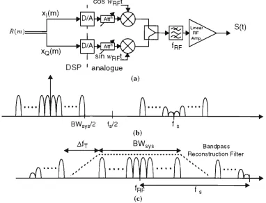
Digital signal processing provides flexibility in the combining process, but the computational requirements are shown to be high, and thus must be minimised. This can be achieved by combining the channels at baseband with efficient algorithms which is investigated for radio base station applications using two current radio system standards.
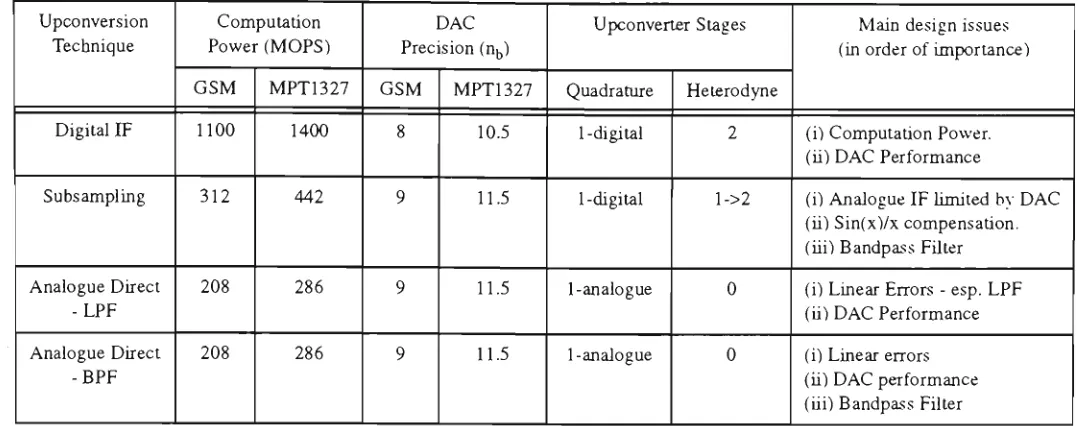
The remainder of the Chapter deals with the upconversion of the baseband multichannel signal to RF. Four upconversion techniques, currently used in single channel applications, are investigated for use in a multichannel environment. A comparison reveals that the analogue direct upconversion technique currentiy provides the most attractive solution because it requires less computation and a lower performance digital to analogue converter (DAC). The disadvantage with this method is that it requires accurate phase and gain matching in the analogue quadrature circuits.
The reconstruction filters cause frequency dependence in the quadrature circuit. These frequency dependent imbalances, and the effect they have on a multichannel signal, are analysed in Chapter 4. A novel adaptive correction method for these imbalances is also presented. Its main advantages over previous adaptive compensation techniques is that UTiplementation occurs at the lower channel samphng frequency and that frequency dependent imbalances can be corrected.
Multichannel radio systems can only tolerate very low harmonic and intermodulation (IM) products. The Digital to Analogue Converter (DAC) is a major source of these spurious responses which can be reduced by adding a dither signal to the multichannel signal prior to quantisation. This issue is discussed in Chapter 5.
Chapter 6 presents a new technique for implementing bandlimited dither. The technique improves the performance of the DAC by 2 to 4 dB, with a minimal increase in hardware. Measurements highlight the benefits of the bandlimited technique over the more traditional wideband techniques. The dithering algorithm was also implemented on an integrated circuit.
Base Station Transmitter Architectures
2.1 Introduction
Early wireless communication systems, TV and radio, used a single antenna per transmitter. The rapid growth of TV and radio through the 60's and 70's, and mobile radio in more recent times, placed enormous pressure on finding suitable transmission sites, especially in high density areas. The expansion of radio systems also saw the increase in antenna structures, which started to come under attack from the populace for aesthetic reasons.
Multiple antenna sites created technical difficulties from the point of view of spurious, intermodulation and noise emissions. This invariably resulted in the blocking or desensitising of the co-sited receivers which led to a degraded system performance. The sum of all these pressures resulted in the science of antenna combining (multicoupling), which is the transmission of a number of similar frequency channels through a single antenna.
Two different systems have been chosen as examples of typical radio communication systems.
MPT1327 is a Private Mobile Radio (PMR) trunking system that was developed by Philips (UK), and adopted in Australia. PMR trunking systems are utilised by private users, such as taxi, train, and fleet orientated specialists, or by the public emergency service sector, such as the police, ambulance, fire, electricity and water providers.
• Global System for Mobile communication (GSM) is a digital cellular European standard that has been adopted by a large niunber of countries, including Australia. It is already in operation in the 900 MHz band. A system with a virtually equivalent specification has been designed for the 1800 MHz band, and more recentiy the 1900 MHz band in the USA. This system is called DCS or Personal Communication System (PCS).
Section 2.2 introduces the main components of the conventional base station transmitter architecture, and describes how each contributes to the architecture satisfying the radio system design specifications. The multicoupling network is shown to limit the performance of the architecture in terms of flexibility, size and minimum channel separation. These limitations will be explored further in the Section 2.3.
Section 2.4 introduces both an analogue and digital low power combining architecture which makes the high power multicoupling network redundant; the digital solution is shown to be more flexible than the analogue solution. The remaining Section of this Chapter discusses the advantages and technical challenges of the low power combining digital signal processing architecture. The technical challenges provide the basis for the thesis.
2.2 Conventional Base Station Transmitter Architectures
A typical base station transmitter has a channelised architecture that complements a Frequency Division Multiplex (FDM) communication system. That is, each channel undergoes separate modulation and amplification before being combined onto a single antenna.
RF Modulator Power Ferrite Amplifier Isolator Tunable Critical SD Cavity Resonator Harness Filter
Information \ ^ /
Figure 2.1: Conventional multicoupling base station transmitter architecture.
2.2.1 Modulator
The modulator encodes the source information onto a bandpass signal with a centre frequency of fj^. The generic single modulated channel can be written as:
Sk(t) = ak(t) cos( 27ufkt+ek(t)) (2.1)
where ak(t) is the amplitude modulation, f^ represents the centre frequency of the channel, and 0jj(t) the phase modulation.
2.2.2 Power Amplifier
The Power AmpHfier (PA) increases the level of the modulated signal whilst limiting the amount of distortion generated. The distortion allowed is set by the specifications of the radio system. This specification covers the region of the spectrum within the channel being amplified, 'in channel', and also the region adjacent to the channel in question, 'out of channel'.
The effect of 'in channel' distortion will be to degrade the noise margin of the link. This is very important in low noise margin systems with dense signal constellations, such as satellite and fixed microwave links, but has littie effect on the performance of mobile systems that require higher noise margins to overcome fading and interference effects.
signal. 'Out of channels' signals must therefore be tightiy controlled. The specification of the spectrum resulting from the modulation and amplification is usually given in the form of a modulation mask. Examples of modulation masks for a trunking radio system. MPT1327, and a cellular radio system, GSM, are shown in Fig. 2.2(a) and Fig. 2.2(b).
dBm i 45(47)
Adjacent Channel
6.25 18.75 Offset frequency
from carrier(kHz)
Figure 2.2(a): MPT1327 modulation mask for 12.5 kHz channel spacing and 50 W (47 dBm)
average output power. The measurement bandwidth is 8.5 kHz (45 dBm) [11].
Note that the modulation mask is most important in the region of the carrier. The multicoupling network will have little or no control in this region. The primary role of the mask is then to specify the allowable Adjacent Channel Interference (ACI). The vertical axis on Fig. 2.2(a) shows the total power level of the channel written in the parenthesis, whilst the other value is derived from the fact that the measurement filter is specified as having 8.5 kHz bandwidth. Consequentiy, if we assume that the whole channel is equally activated, only a proportion (8.5/12.5) of the actual power will be measured using this filter.
The ACI specification for the trunked radio system is very stringent, 55 dBc from Fig. 2.2(a). This is due to the near-far^ problem where the physical location of each base station is uncontrolled and where higher power levels are used to broadcast signals across large areas (compared to cellular systems).
1. "Ilie adjacent channel interference refers to "that part of the total power output of a transmitter under defined conditions of modula-tion, which falls within the specified passband centred on the nominal frequency of that of the adjacent channels. This power is the sum of the mean power produced by the modulation, hum and noise of the transmitter" [11]
Cellular systems. Fig. 2.2(b), allow for a weaker ACI specification of 30 dBc. primarily due to the controlled nature of their operation. That is, blocks of frequency are allocated to a specific system, and the use of frequency planning means that adjacent channels are not transmitted concurrently in the same basestation (cell). Neighbouring channels (2 or more channels from the carrier centre frequency) are well protected. For these channels the specification becomes between -60 dBc and -70 dBc.
Different power classes of transmitters are also highlighted in Fig. 2.2(b). GSM specifies 8 classes ranging from TRX 1 (55 dBm) through to TRX8 (34 dBm). This accounts for different cell sizes, ranging from large cells (TRX 1) to small cells (TRX 5) and down to micro cells (TRX 8). The base station can also utilise downlink RF power control. This consists of 15 power steps in 2 dB increments (30 dB), and has the effect of incrementally moving the mask through the shaded area as shown in Fig. 2.2(b). The measurement bandwidth for GSM is specified as 30 kHz and power levels using this bandwidth are shown prior to the parenthesis.
dBm
46.8(55)
34.8(43) 25.8(34)
4.8(13)
TRX1
TRX5 1 \ TRX 8 ' \ \
\ \ ^
1^ ' ^
i "> i 1
ACI H 30 dBc 1
L 1
k
70 dB
r
1 x^^^^""-^---^
* ^ i « - "
Channel 1 ^?J^^®"! 1 Neighbouring channels Channel ^
'^ „ ^
Power Control Range
^ •
100 200 400 600 Offset frequency from carrier (kHz)
Figure 2.2(b): GSM modulation masks for three transmitter power output classes; TRX 1
2.2.3 Ferrite Isolators
Reverse leakage can allow signal power from transmitters on the same combining network, or signal power directly received from the transmitting antenna, to enter the output of another channel's power amphfier. The mixing of the wanted and reverse interference signals in the power amplifier will generate unwanted InterModulation (IM) products. A vital component in the protection of the power amplifier from the reverse interferer is the unidirectional characteristic of the ferrite isolator.
Carrier @ f
Output Signal
Mini Ccts Amp ZHL-42
Gamp = 30dB
(a)
Reverse Interferer @ f|
(PREV)
^amp Pc
P|M3
i L "reflect i L
2fc-fi tc fi
(b)
P|M3
t ,
2frfc
-35 - 3 0 - 2 5 - 2 0 - 1 5 - 1 0 Reverse Interferer Signal (dBm)
(C)
Figure 2.3: (a) Reverse interferer arriving at the output of the amplifier and mixing with
the carrier to create an output spectrum consisting of IM products, (b) Spectrum of the amplifiers output signal (c) Reverse interferer (P^Ey) plotted against the dominant third order intermodulation product (PJMS)- Class A amplifier operated at its 1 dB compression
point, G^^p.P^ =30 dBm.
The ferrite isolator attenuates the amplified signal, travelling in the forward direction, by a nominal amount (-0.5 dB), whilst the interfering signal, travelling in the reverse direction, is significantiy attenuated (-25-50 dB [14]). The amount isolation is related directiy to the intermodulation attenuation specification, which is specified as 70 dBc for both the GSM and MPT1327 radio systems.
Calculation of the exact amount of isolation requires knowledge of the relationship between the return interfering signal level and the resulting intermodulation product level at the output of the amplifier. Fig. 2.3(a) illustrates the situation more precisely assuming that the amplifier has a dominant third order characteristic. The amplifier's output signal. Fig. 2.3(b), consists of a wanted carrier P^, amplified by the gain factor G^^^p, an interferer ^reflect' which is directly related to the output reflection coefficient of the amplifier, and the third order products PJMS^ caused through the mixing of these two signals.
The relationship between the reverse interferer, PREV' ^^'^ '^he dominant third order
intermodulation product, PIMS. was measured for a 'Mini Circuits' class A amplifier with a rated output power of 30 dBm. This is plotted in Fig. 2.3(c) and it shows that the relationship can be accurately written as:
PlM3=PREV-18dB (2.2)
Thus to achieve an intermodulation specification of 70 dBc (-40 dBm), the reverse travelling signal incident on the amplifier must be no larger than -22 dBm.
There are two possible sources of interfering signals: those that come from transmitters on the same combining network, and those directiy received from the transmitting antenna. For the transmitters on the same combining network, the amount of reverse power arriving at the transmitter in question is:
PREV = PC + G ^ p - TX-TXi,,i,^i,„ dBm (2.3)
where the transmitter to transmitter isolation, TX-TXjsoiation' is giyen by the following formula [14]:
TX-TXisoiation - I^isolator + ^^cavity "*" ^cavity "*• ^isolator "•• ^cable + " dB (2.4)
where ILisojatop ILcavity = the insertion loss of tiie isolator and cavity, Lcabie= cable losses ^ d lisoiaton ^cavity = isolation of the ferrite isolator and cavity filter. Given that the carrier input power is 0 dBm and tiie gain is 30 dB, tiien from Eqn. (2.3) the amount of TX-TXisoiation required is 52 dB.
PREV = Pant-lm " ^^^T-TXisoiation (2-5)
where Pant-int is the interference power received at the antenna and the amount of antenna to transmitter isolation is given by:
AN 1-1XjjQi^jjQjj = Icavity "*" ^isolator "•" ^feeder "^ Lcable ^^ (2.6)
where Lfee^gj. = the loss of the feeder. Given that the typical test interferer power received at the antenna [11], Pgnt-int' is -30 dBc (0 dBm), the amount of ANT-TXisojation calculated from Eqn. (2.5) is 22 dB, significantly lower than the required
TX-TXisoi^tion-The amount of TX-TXjsoiation required for the GSM or MPT1327 (same intermodulation attenuation specification) multichannel systems is therefore determined from a neighbouring transmitter on the same combining network. The value, 52 dB, calculated is somewhat small compared to the 70-80 dB of TX-TXisoi^jjojj quoted as a typical requirement [14]. The difference can be attributed to the use of higher power amphfiers with class C output stages and a more stringent intermodulation specification.
For the class C amplifier the dominant intermodulation product is typically only 6 dB smaller than the reverse interference signal. Eqn. (2.2) is subsequentiy modified for a class C amphfier such that the amount of TX-TX isolation required is 64 dB. This value will be further increased for a more stringent intermodulation specification such as that defined for the maximum spurious level (this is discussed Section 2.2.4.2).
The ferrite isolator is a very important device in the conventional base station architecture because it is used to provide a significant proportion of the required 70-80 dB of TX-TX isolation. Only small quantities of isolation are contributed by the other components of the TX-TX isolation equation, Eqn. (2.4).
2.2.4 Multicoupling Networks
The number of channels combined onto one antenna (N^omb) is dependent on the system. For the GSM cellular system, with a cell reuse factor of 3 and cells that are split into 3 sectors, then each sector antenna will only be assigned 1/9 of the total channels available in the system. For a system bandwidth of 5 MHz and a 200 kHz channel separation, this directly computes to 3 combined channels per sector. Currentiy, a fuUy configured GSM cell site has 4 channels combined onto one anteima. However, in the future, the introduction of frequency hopping will decrease the cell reuse factor, subsequentiy increasing the number of channels combined on to the antenna. On the other hand, the combining requirements for the MPT1327 system are inherently limited by the minimum transmitter spacing of the cavity combining networks; for a 12.5 kHz trunking system the minimum transmitter separation is approxiamately 200 kHz. Thus it is possible that up to 25 channels could be activated across a 5 MHz bandwidth, although current systems typically combine between 5 and 10 channels.
RX BAND
/ • • • • • / / / > .
SD Filter Response
Cavity Resonator Response
Isolation
Channel Separation
. e i ^
(c)
SOURCE
Coupling
to
(d)
Coupling
I
£
in
c CO
LOAD
1:n W m:1
Figure 2.4: (a) The response of the Cavity Resonators and Spectrum Dividing (SD) filters,
Once combined, and as a final measure to ensure that no interference problems will exist, the signal passes through another cavity resonator covering the total transmitter bandwidth. This resonator is used to reduce the transmitter's noise floor (consisting of broadband noise and spurious products [2]) so that there will be no interaction with other systems or nearby receivers, which may or may not be connected to the same antenna. They are commonly referred to as Spectrum Dividing (SD) filters since they isolate different segments of the spectrum (as shown in Fig. 2.4(a)).
2.2.4.1 Cavity Resonators
As depicted in Fig. 2.1, each amphfied channel is fed into a cavity resonator which is manually tuned through the means of a tuning stub or screw. The output of each cavity filter is then coupled into a single output through a critical harness. The critical harness acts as an impedance transformer, so that the cavity only loads the antenna when resonant.
The behaviour of a cavity resonator is analogous to that of a parallel resonant circuit. Fig. 2.4(d), in the vicinity of resonance, with very high Q values (high selectivity) and low insertion loss. Coupling into and out of the cavity is modelled as an ideal transformer. At resonance both the source and load see an impedance that is dependent on the couphng coefficient into and out of the cavity. It will not be necessarily matched to the source or load impedances.
The transfer function, H^^^^^yiAf), of the resonator can be approximately modelled near resonance as:
I H,avity(Af) I = 10 log (1+ (2.Af / BWeavity)^ ) dB (2.7)
where Af is the offset from the centre frequency, f^, and BWcavity is the 3 dB bandwidth of the cavity. The bandpass response will suppress the IM products, broadband noise and spurious products, but it is not selective enough to affect the responses in the adjacent channel or neighbouring channels (as mentioned in Section 2.2.2).
The selectivity of the resonator is directiy related to the loaded Q, QL, of the cavity:
Q L = fc / BWeavity (2-8)
BWcavity = 600 kHz @ 900 MHz for GSM, QL= 1500. Given that tiie insertion loss of tiie cavity is approximately (see Appendix A.1):
IL^avity = -20 log (1- Q L / Qo) dB (2.9)
The unloaded Q (Q^) must be sigiuficantiy greater than QL- To keep the insertion loss lower than 1 dB, Q^ must be at least a factor of 8.2 greater than QL- The design of cavities is therefore based around attaining large values of QQ. QQ is fundamentally defined as:
Qo = 27t:f . energy stored / power dissipated (2.10)
The volume and the surface area are the mechanisms that store and dissipate energy respectively. Therefore, the dimensions of the cavity, the use of high quahty materials (such as silver or copper) and the use of advanced fabrication techniques [15] are important parameters to achieve large QQ values. As a result, high quality cavities are expensive, voluminous and heavy.
In the UHF band, the most common kind of cavity is the quarter wavelength coaxial cavity, operating in TEM mode [3]. These cavities achieve good temperature stability, high unloaded Q (QQ) values of between 5000 - 10,000 and are relatively compact.
At lower radio frequencies i.e. the VHF band, where the physical size of a quarter wavelength cavity becomes large, electrically short coaxial cavities, helical resonators and lumped LC circuits (although these are only practical at the lower end of the VHF spectrum) become favourable. Helical resonators usually provide Q^ factors of up to 1000. They can also be used at higher frequencies where they usually perform as wideband spectrum dividing filters.
2.2.4.2 Spectrum Dividing Filters
The spectrum dividing filter follows the physical channel combination stage. It serves to attenuate broadband noise and spurious emissions generated by all the prior processes. Spurious emissions are "emissions at frequencies other than those of the carrier and sidebands associated with normal modulation" [11]. They are usually specified as an absolute power level (nominally 0.25uW) measured in a certain measurement bandwidth, and are a more stringent requirement than either the spectrum mask or intermodulation attenuation specifications. Additionally, spurious levels are specified at large frequency offsets from the carrier, as depicted in Fig. 2.5(a).
Both Figs. 2.5(a) and (b) are normahsed to a measurement bandwidth, 30 kHz and 8.5 kHz for GSM and MPT1327 systems respectively. The power is written with respect to the measurement bandwidth, whilst the power figure given in the parenthesis indicates the total output power of the channel. Note that the spurious emission level specification takes precedence over the other specifications. For example, if power control was implemented for GSM, the lowest level for which the 8* class transmitter (TRX 8) could take would be 4.8(13) dBm. Interference into neighbouring channels should be below -55.2(-47) dBm as defined by the modulation mask, Fig. 2.5(a), a level substantially below that of the specified spurious emission level, -41.2 dBm. It is in this situation that the less stringent spurious emission specification would apply.
dBmA 25.8(34
4.8(13).
67 dBc
dBmi
45(47)
-37
100200 400
Modulation Mask 600
(a) 1800
Spurious emission • ISVel specification
6000 Offset frequency from carrier (kHz)
82 dBc
Spurious emission ,^ level specification
V
Bandpass Duplexer
From Transmitter
I
To Receiver
(c)
1000 Offset frequency /u\ from carrier(kHz)
Figure 2.5: (a) GSM modulation mask and spurious emission level normalised to a
measurement bandwidth of 30 kHz [9]. (b) MPT1327 modulation mask and spurious emission level normalised to a measurement bandwidth of 8.5 kHz [11]. (c) Spectrum dividing (SD) filters used in a bandpass duplexer.
2.3
Limitations of a Conventional Base Station Transmitter
2.3.1 Minimum Chamiel Separation
Future wireless systems have requirements that are based around frequency agihty. frequency hopping and dynanuc channel allocation. Many more channels will therefore have to be available for transmission, although not necessarily all at the same time. The nature of cavity resonators place fundamental restrictions on the minimum channel separation, which limits the number of channels that can be combined onto a single antenna. As the channel spacing between the cavities is reduced the insertion (power) loss increases and the isolation between adjacent transmitters (TX-TXisoiation) decreases.
As the channel spacing is reduced, the isolation between transmitters will decrease assuming that the cavity is operating at a fixed QL- Ferrite isolators can be used to compensate for the lost isolation however, it is the problem of increasing insertion loss due to cavity loading of closely spaced transmitters that is more serious.
It is assumed that Ncomb channels are to be combined onto a single antenna. As illustrated in Fig. 2.6(a), each transmitted channel gets fed through an isolator, cavity resonator and quarter wavelength line, before being combined at a common point. The quarter wavelength line acts as an impedance transformer (see Appendix A.3).
(a) (b)
Figure 2.6: (a) Multicoupling N channels onto a single antenna (b) equivalent circuit
The couphng of the cavity is assumed to be arranged so that the output admittance of the cavity is matched at resonance (special case of Appendix A.2 where RRES = Zo). The admittance, as a function of Af, of a single cavity looking from the junction point (i.e. after the quarter wave transformation) is given by:
Ycavity = VI Yout = d/Zo)' / ( d + 2Af / B W,,,i,y) IZ^) (2.11)
The equivalent circuit has been drawn such that the network is under consideration at the resonant frequency of one of the cavity resonators. Therefore, the admittance of the resonant cavity, Y^-ayi^y, is equal to l/Z^ (from Eqn. (2.11) when Af=0). The antenna is also assumed to be matched to the characteristic impedance, ZQ, whilst YQ„^ refers to the equivalent admittance of the remaining (Nj,ojj^,3-l) cavities (Fig. 2.6(b)).
The amount of insertion loss that the channel under consideration undergoes is equal to the insertion loss of the cavity itself (fL^avity as defined in Eqn. (2.8) ) and the insertion loss caused by the power absorbed in Ygny (see Eqn. (A.22) in Appendix A.4). Total insertion loss is therefore defined as:
IL = 20 log(l-QL/ Qo) + 10 log( ( l + r ) ( l + r ) * ) dB (2.12)
where the reflection coefficient is given by (see Eqn. (A. 17) in Appendix A.4):
r =-Yeq, / (2Y,+Yeq„) (2.13)
When only one resonant cavity is connected to the antenna, Ygqy = 0 and the total insertion loss is given by that of the cavity itself. The effect of adding more and more cavities to the antenna results in Y^^u being non zero as described below:
(W„„,-2)/2
ri= 1
Ye,u = I Yca.ayi" ' ^fcs) + >'c.v,,v(-" ' ^f Cs) + >'cav,;J " f ^ ' ^fcs] ^c.,„fc ^ ^ ^ ^ (2- 1 4 a )
Ye,u = I Yca.i.yi'^ ' ^fcs) + Yca.Uyi'" ^f Cs) ^comb odd (2.14b)
« = 1
100 200 300 400 500 600 700 BOO 600 1000 NormaIis.d Chann«l Spacing {KHz)
! i 2 -
Tl'-eys
j ^ ^ ' * :
IL:
. ^ "l-cavity
" •
1500
Load«dQ
(a) (b)
Figure 2.7: (a) Total insertion loss (IL) for l^comb combined channels. System parameters
Qo = 9000, fo = 450 MHz &QL= 1800 (b) Total insertion loss (IL) = IL^ayHy + IL^qu, as a
function of the Loaded Q. N=3 and channel spacing = 500 kHz.
In the case when the channels are spaced by large frequencies, Y^^^ will be neghgible (i.e. open circuit for all resonators at the frequency of consideration) and the additional insertion loss will also be small. As the channel spacing is reduced, the adjacent cavity circuits will take on finite values of impedance rather than look like open circuits. This creates a mismatch at the junction causing both reflection of power and power being absorbed by the loading of the other cavity circuits. The overall effect is that less power will arrive at the antenna.
As the channel spacing is further reduced the effect is amplified. Immediately adjacent channels have a more significant effect on Ygqy, and the other neighbouring cavity circuits also begin to make contributions. Fig. 2.7(a) shows that the insertion loss rises rapidly as the channel spacing is reduced. The effect is further pronounced as more channels are combined onto a single antenna.
and ILgqy. The total insertion loss curve results in an optimum setting of coupling (QL = 1500), to achieve a minimum amount of insertion loss.
Although measures can be taken to minimise the insertion loss, the amount of insertion loss that can be tolerated within a given system will still restrict the minimum channel spacing. This is a hmitation of the conventional transmitter architecture.
2.3.2 Frequency Flexibility
Frequency agility is the abihty of a system to rapidly and easily change the channel frequency, it is seen as an integral component in enhancing the capacity of future radio systems. For example, the technique of frequency hopping requires the transmitter to change from one carrier frequency to another in some pre-determined hopping pattern. The GSM radio system specifies 216.68 hops per second [11]. Frequency agility is also required to cope with the dynamic load changes within a system. Examples of areas which may experience large load changes are the main arterials during rush hour, and the CBD during working hours. Future systems will incorporate flexible frequency plans that require the dynamic allocation (daily, hourly or even instantaneous changes) of channel frequencies on a continual process.
The conventional base station architecture as discussed in Section 2.2 has very limited frequency agility due to the manual tuning mechanism. The architecture can be extended to achieve limited frequency agility, however, through the use of electro-mechanical tuning resonators and the dual windows approach. This is at the expense of increased complexity and cost. Replacing the cavity resonators with a hybrid combiner can achieve unbridled frequency agility but this technique is very expensive in terms of lost signal power.
2.3.2.1 lYmable Cavity Resonators
Electro-mechanical tuning resonators are used in the case of a system requiring regular re-calibration or remote re-tuning of the cavity to a new transmit frequency.
are various techniques for the rapid re-tuning of resonators [17]. The tuning range varies between 0.05% - 1% of the centre frequency with a degradation in unloaded Q value of around 50%. Although tuning times in the order of microseconds are achievable, electro-mechanical resonators usually take between 0.1 - 10 seconds to tune [4].
2.3.2.2 Dual Window Cavity Combiner
Another technique for making the cavity resonator solution somewhat more frequency agile is the dual window combiner. Fig. 2.8(a). This combiner utilises fixed tuned window filters arranged so that by interleaving two electrically de-coupled sets, continuous coverage of a dedicated portion of the spectrum can be obtained [4], Fig. 2.8(b).
Even Group
Hybrid Combiner
Odd Group
(a)
1.2 MHz Odd Group P Z
Passbands ///// Even Group
Passbands
Vy
^
b^
2
V.
N ^
I ^
^ O k H z 12.5 MHz
(b)
Figure 2.8: (a) Dual window cavity combiner architecture (b) Diagram displaying nominal
frequency values for the dual window cavity combiner
Each window utihses two X/4 cavity resonators to give an overall four pole (bandpass) filter response to maintain sufficient isolation between the adjacent channels in each window. The bandwidth of each window is approximately 600 kHz, 3 channels (@ 200 kHz) for GSM or 48 channels (@ 12.5 kHz) for MPT1327. Two groups, an even and an odd, are made up of 19 of these windows coupled togetiier. The two groups of filters are coupled to a single antenna by means of a 3 dB coupler. The overall transmitter to antenna loss is 5.2 dB, about 1.4 dB greater tiian the conventional architecture [4].
continuous, making it more suitable for cellular systems than for other radio systems where the spectrum is not allocated in a dedicated block.
2.3.2.3 Hybrid Combining
A technique of combining very closely spaced transmitters (i.e. less than 100 kHz), is performed through the use of a high power hybrid combiner. Fig. 2.9. There are many different hybrid topologies [8] that can adequately perform the combining process. However, they will all exhibit an insertion loss that varies depending upon the phase and amplitude of the input signals [8]. If the signals are uncorrelated, then the theoretical average insertion loss that each input undergoes is lOlog^oNcomb' where N^omb i^ ^ c number of signals being combined. Obviously this is very expensive in terms of lost power, and this constitutes the major disadvantage of hybrid combining.
RF Modulator A ^ S i e r Circulator High Power SD Hybrid Combiner '^''*®'' v i ^
Information
Figure 2.9: Hybrid Combining Base Station Transmitter Architecture
A significant advantage of hybrid combining over conventional combining is the ability to
combine channels with no restrictions on channel spacing. However, to maintain high isolation between ports, it is very important to have a well matched output port. With accurate manufacturing of the hybrid, only 35 dB of isolation is achievable [2] and so ferrite isolators will still be needed to achieve the required
TX-TXjgoiation-2.3.3 Size
system, the volume per channel of a base station was reduced by a factor of around 4 between 1985 and 1990 [13]. If forecasts hold true, the volume of base stations must continue to be considerably reduced so that the number and area of basestation sites do not expand at the same rate.
The open market approach to wireless communications, adopted worldwide, allows for new private operators to compete against the established telecommunication operators. These operators will also require premises for their infrastrucmre. This will place enormous pressure on sites in urban environments. Small base stations will be highly desired to keep site costs minimal.
Future wireless systems, especially cellular, also make provisions for hierarchical cell structures that consist of very small cell sizes, micro and pico. An unobtrusive base station might be located on a lamp post, in a mall, or in the comer of an office. It wifl have a major aesthetic requirement, which will again most easily be met by small size.
Cavity resonators account for the considerable volume in the conventional base station transmitter. Typically they take up around 30% of the rack space. As highlighted in Table 2.1, the volume and weight of a cavity resonators is very significant. The removal of cavity filters from the architecture will result is considerable size and weight reductions.
Table 2.1: Nominal Cavity Resonator Data [19]
Frequency Band (MHz)
420-512
900 MHz
Resonator Type
X/4 coaxial
X/4 coaxial
Volume (m^) / Channel
0.05
0.01
Weight / channel
6 Kg
2.4 Low Power Combining Base Station Transmitter Architecture.
By using a low power combining scheme, followed by a high power, hnear and wideband amphfier a significant improvement can be achieved in terms of flexibihty and performance. The concept essentially involves the removal of the voluminous and inflexible cavity resonators, and a subsequent rearrangement in the amplification and combining processes. The low power combining can occur in either an analogue or digital environment, giving rise to two architectures, hybrid combining or digital signal processing combining.
2.4.1 Hybrid Low Power Combining
The low power hybrid combiner architecmre [5,6a,6b,20], as opposed to the high power hybrid combiner (Section 2.3.2.3), combines the analogue radio frequency outputs of the individual channel modulators. The modulators are the same devices as those used in the conventional combining architecture. A well designed hybrid combiner provides 35 dB of isolation. If this isolation is not sufficient to limit intermodulation then additional isolation can be easily provided by circulators and low power amphfiers with good reverse isolation.
RF Modulator Low Power Hybrid Combiner
Wideband Power Amplifier
Spectrum Antenna Dividing
Filter
Information
P A > — •
- •Figure 2.10: Hybrid low power combining in the analogue environment.
The wideband amplifier has been the major technological obstacle. It has low DC-RF efficiency, high cost and limited total output power. The most important problem, however, is that the necessary linearity specifications are hard to meet To achieve sufficient linearity from the amplifier, the technique of 'back-off has traditionally been used [5,6a,6b]. However, in a multichannel situation, the DC-RF efficiency is consequently very low, and a large back-off will mean that the amplifier becomes expensive mainly due to the large amount of over-rating required. Linearisation techniques are seen as a means of improving the DC-RF efficiency and lowering the device power rating. Extensive research has been carried out into the linearisation of wideband amphfiers, utilising techniques such as predistortion and feedforward. Commercial solutions are now becoming available for small cell sizes.
2.4.2 Digital Signal Processing Combining
The combining can also be implemented in a digital signal processor. This further increases the overall flexibility of the design by incorporating the modulating and combining tasks together in a common processor under complete software control. Ultimately the DSP solution would mean a single hardware platform for the implementation of a generic base station architecture.
Modulator & Combiner
Wideband Upconverter Power
Amplifier
Spectrum Antenna Dividing
Filter
Information w
w
^
w
Ik
^
W
Digital Analogue
Figure 2.11: DSP low power combining in the digital environment.
2A.1.1 Advantages of DSP Combining
Software Flexibility
The digital signal processor is inherentiy flexible because the functionality is programmable. That is, the modulation format or channel frequency can be dynamically changed by selecting a different subroutine or variable. It is technologically feasible to produce a generic base station for many different radio system standards.
High TX-TX Isolation
The transmitter to transmitter isolation is set by the precision of the DAC and DSP, because the modulated channels are combined in a DSP environment. It can be easily controlled by ensuring sufficient precision in both components.
Low Power Loss
Any power loss that occurs after amplification is critical as it increases the effective power rating of the amplifier. In the conventional architecture, a significant amount of power loss occurs due to the cavity resonators, isolators, SD filters and cable loss. Combining at low power levels means that the power loss after amphfication is somewhat smaUer, equal to that of the SD filter and the cable only.
No Restrictions on the Minimum Channel Separation
The cavity resonators restrict the minimum separation between channels in the conventional base station transmitter architecture. In the DSP low power combining architecture no restriction exists and all channels within a given bandwidth can be combined and transmitted simultaneously. Channels with different bandwidths and/or modulation schemes can also be combined. The inherent flexibility of the DSP combining architecture therefore lends itself perfectiy to implementing future frequency agile systems.
Silicon Integration
Cost of Equipment and Maintenance
Removal of the expensive precision made cavity resonators from the base station architecture will contribute to a reduction in the cost of equipment. In addition, maintenance (calibration) and re-tuning of the cavities requires a technician to make a site visit to mechanically tune the cavities. This process is both time consuming and expensive, especially if frequency re-planning of the radio system occurs regularly.
2.4.2.2 Challenges of DSP Combining
Multichannel Combining
A number of channels will require both modulation and combination, and this could occur across a bandwidth of up to 50 MHz. Consequentiy the computation load will be large. Efficient algorithms for the combining and modulating process are an essential element for practical implementation in a DSP environment. The output samphng rate of the digitally produced multichannel signal will also place large demands on the digital signal processor. Chapter 3 will investigate efficient DSP combining algorithms.
DAC Interface
The high precision and speed requirements of the DAC interface have always been considered a limitation of the DSP architecture. This is primarily because the high speed requirements correspond to lower precision commercially available devices.
The performance of the DAC is measured by the Signal to Noise Ratio (SNR) and the Spurious Free Dynamic Range (SFDR), both of which are degraded by static and dynamic errors of the device. These errors will generate harmonic and IM products that will fall into neighbouring channels, and can exceed the stringent spurious emission specification. Fig. 2.5(a) & (b). A technique for improving the SFDR will be introduced in Chapters 5 and 6.
Frequency Conversion to RF
Upconversion to RF will incorporate either quadrature or heterodyne techniques, or a combination of both.
undesired sideband signals that will faU into a neighbouring channel. In addition, both quadrature and heterodyne upconversion stages incorporate mixers, which are nonhnear devices. Subsequently, the multichannel signal will generate intermodulation components, or more unwanted spurious responses. The different spurious signals will invariably fall into neighbouring channels, and therefore must not exceed the spurious emission
specification of the particular system.
Intermodulation caused by mixer nonlinearity can be controlled by incorporating high intercept point mixers and lowering the input signal level into the mixer. This does not present any serious technical problems [6b], however the amplitude and phase errors of analogue quadrature upconverters require correction. A novel compensation circuit will be introduced in Chapter 4.
Wideband Ultra-Linear Power Amplifier
The wideband power amplifier is a major technical challenge because of the problems of non-linearity and power output. The nonlinearity of the amplifier will produce intermodulation components which must not exceed the system specification. From Fig. 2.5(a) (GSM, power class TRX8) tiie spurious emission level must be at least -61.8 dBc within 6 MHz of the carrier, and from Fig. 2.5(c) the MPT1327 requirement is in the order of -82 dBc spurious rejection. The spurious rejection must be consistent across a wide bandwidth; therefore, ultra-linear amplifier behaviour is required. This is technologically feasible as an amplifier in the 900 MHz cellular band has been reported to suppress third order products to 70 dBc over a 5 MHz bandwidth [7].
The maximum power output level achieved by wideband, ultra-linear amplifiers also presents a major technical obstacle. This is aggravated by the fact that the peak power level of multichannel signals significantly increases the total power rating of the amplifier. For example, if N^omb channels are shnultaneously activated at an average power of P^y, the total average power of the Ncomb channels is:
Ptav = Ncomb • Pav (2-15)
having an average channel output of 20 watts (GSM power class TRX5), the PEP is equivalent to 320 Watts. A good linear amplifier has intermodulation products 30 dB down at rated power [5] given that the third order distortion is dominant. Therefore to achieve -72 dBc of spurious rejection, the amplifier must be operated at a backoff of 21 dB. The rated power of the amphfier required for combining 4 channels would therefore be 40,000 Watts! For the PMR trunking system with more combined channels the situation is even worse.
A way of decreasing the effective rating of the amplifier is to linearise the amplifier. Currently commercially available feedforward linearised amplifiers obtain in the order of 60-65 dBc suppression of intermodulation products at up to 25 Watts of total average power [Microwave Power Devices feedforward amplifier]. For a 4 channel system this amounts to 6 Watts of average power per channel, matching only the 7* (TRX7) and 8^*^ (TRX8) power class specifications in the GSM base station transmitter.
It is obvious that high power transmission, using a low power combining architecture is restricted by the practical size of the ultra-linear amplifier. Current amplifier technology is capable of meeting only low power outputs, synonymous with small or micro cells. Therefore, this thesis will consider the GSM TRX8 transmitter specification as an example of smaller sized cells and the MPT1327 radio system as an example of a larger sized cells. The wideband amplifier will not be considered any further.
2.5 Conclusion
This chapter has discussed the conventional base station transmitter architecture, central to which is the cavity resonator. It has been shown that the cavity resonators hmit the flexibihty and minimum channel separation of the transmitter and they are also very large and heavy. A low power combining architecture has been introduced to overcome these hmitations. It rearranges the amplification and combining processes in order to eliminate tiie requirement for a voluminous and inflexible cavity filter.