AN EFFICIENT ADIABATIC FULL ADDER DESIGN
APPROACH FOR LOW POWER
Baljinder Kaur
1, Narinder Sharma
2, Gurpreet Kaur
31
M.Tech Scholar (ECE),
2HOD (ECE),
3AP(ECE)
ABSTRACT
In this paper authors are going to compare the full adder using TG with full adder using energy recovery logic
PFAL.Eventhough transmission logic is very efficient in power consumption but adiabatic technique PFAL is
also a energy reused method. By adiabatic technology, charge stored on node capacitance can be recycled back
and used as power clock. The full adder designed with positive feedback adiabatic logic has better performance
than previous design and all results were verified with Tanner V.7. Various types of parameters such as power
dissipation, transistor count and power supply were compared of both methods on T-Spice tool.
Keywords: Adiabatic Logic, Full adder using TG and PFAL, PFAL, TG, T-SPICE.
I. INTRODUCTION
As in designing of conventional static and dynamic CMOS logic, the circuit performance is necessary in parameters of logic levels, input supply but not in the case of power consumed by the conventional circuits. To obtain less power consumption, the best technique is implemented like reduce the supply voltage, factor .consequently; the design gives us degraded performance [1]. To overcome this problem, the method is introduced works on energy recovery principle known as adiabatic logic. Adiabatic circuits are those circuits in which energy is recycled back to threshold voltage and no energy is wasted [2] .In this paper, author have designed full adder by using adiabatic technique and compare with existing TG design. Before this, I have studied various approaches that are used to minimize the power dissipation of various electronic circuits. Full adder is a circuit which adds three bits and gives the two binary outputs, sum and carry. It is widely used in applications like digital signal processing (DSP), and microprocessor. Different types of full adder were discussed in various papers overthe past decades. The one of the main adders are ripple carry adder, carry look ahead adder and parallel binary adder. In the present paper, the performance analysis of full adder has done with TG logic and adiabatic logic PFAL. In transmission gate logic, the PMOSFET and NMOSFET switches are connected in parallel form and consecutively works as transmission gate. It is observed that high number of internal nodes can increase parasitic capacitances and ultimately circuit complexity becomes increase. So, power consumption of the circuit enhance in many large arithmetic circuits. The circuit design with TG logic is very complicated and takes more delay for logical operation during transition [3].
1.1 Conventional TG Logic
TG stands for transmission gate logic. This method is enforced with terribly minimum transistors as compared to conventional CMOS structure. The PMOS and NMOS are connected consecutively and they behave as a switch and constitute a transmission gate.NMOS transistor pass a signal of binary 0 however a weak 1,inspiteof that, PMOS transistor pass the binary signal 1 however a weak 0[4].
Figure 1 Transmission gate logic [1]
It is the simplest method which combines the properties of both NMOS and PMOS.Both NMOSFET and PMOSFETs are connected in parallel, which leads to a full swing at the output [5].
1.2 Adiabatic logic Principle
Adiabatic circuits are popular due to its lower power dissipation and better performance excepts speed. When capacitive load is charged and discharged, power dissipation occurs. CVDD2 amount of power is dissipated during this process. The term signal energy refers to either the amount of energy stored on the load capacitor (output signal energy) or supplied by the load capacitor (input signal energy) to the next gate. Two types of energy dissipation are: static and dynamic power consumption. Some of energy is consumed in PMOSFET and NMOSFET Switches where resistances offered the voltage drop, second when charge stored on capacitive load is transferred to ground. But the charge which is grounded can be recycled back and gives to power clock, this method is known as adiabatic approach [6].
II. LOGIC DESIGN STYLES
2.1 Full Adder
Full adder is a combinational circuit that performs the addition of 3 binary digits. The input variables are represented by A, B, Cin.A and B represent the 2-input variables and Cin represents the carry from the previous lower significant position. In the full adder, whenever we add two binary numbers, each having two or more binary bits, the least significant bits can be added using half adder. The logic symbol of full adder is shown in “Fig. 2”.
Figure 2 Logic Symbol For Full Adder[7].
Full adder basically accepts 3 inputs and produces 2 outputs sum and carry. As compared to half adder, full adder takes the value of carry input to handle the additional input carries.
Figure 2.1 Logic Diagram for Full Adder [7].
From the Fig 2.1, it is clear that sum(S) is the XOR of A, B and Cin and carry is designed with the combination of AND and OR gate. The output of first exor gate is the input of AND gate and another input Cin is also applied.Similarily, the inputs A and B also applied to the AND gate .As a result, the OR gate gives the result of Carry output [7].
2.2 TG Based Full Adder
Figure 2.2 TG Based Full Adder [8] .
Two TG based ports are used to realize the function of full adder. One is used to implement the sum expression and other for carry [8].
2.3 PFAL Based Full Adder Sum
The PFAL logic consists of a two cross coupled inverters and two functional blocks F and F/. These functional blocks are used for logic operation. The pull up network is designed with combination of NMOS and PMOS. When the inputs a, b and c are at logic 001 and VDD move up from lower position to higher position of constant supply then F-array sum store data one. Sum/ charge the capacitor up to the threshold level. Now VDD fall from higher position to lower position then sum/ gives its energy back to VDD, no energy of VDD is grounded. When the inputs a, b and c are at logic 010 and VDD move up from lower position to higher position of constant supply then F-array sum store data one. Sum/ charge the capacitor up to the threshold level. Now VDD fall from higher position to lower position then sum/ gives its energy back to VDD, no energy of VDD is grounded. When the inputs a, b and c are at logic 100 and VDD move up from lower position to higher position of constant supply then F-array sum store data one. Sum/ charge the capacitor up to the threshold level. Now VDD fall from higher position to lower position then sum/ gives its energy back to VDD, no energy of VDD is grounded. When the inputs a, b and c are at logic 111 and VDD move up from lower position to higher position of constant supply then F-array sum store data one. Sum/ charge the capacitor up to the threshold level. Now VDD fall from higher position to lower position then sum/ gives its energy back to VDD, no energy of VDD is grounded.
2.4 PFAL Based Full Adder Carry
The PFAL logic consists of a two cross coupled inverters and two functional blocks F and F/. These functional blocks are used for logic operation. The pull up network is designed with combination of NMOS and PMOS.When the inputs a, b and c are at logic 011 and VDD move up from lower position to higher position of constant supply then F-array carry store data one. Carry/ charge the capacitor up to the threshold level. Now VDD fall from higher position to lower position then carry/ gives its energy back to VDD, no energy of VDD is grounded. When the inputs a, b and c are at logic 101 and VDD move up from lower position to higher position of constant supply then F-array carry store data one. Carry/ charge the capacitor up to the threshold level. Now VDD fall from higher position to lower position then carry/ gives its energy back to VDD, no energy of VDD is grounded. When the inputs a, b and c are at logic 111 and VDD move up from lower position to higher position of constant supply then F-array carry store data one. Carry/ charge the capacitor up to the threshold level. Now VDD fall from higher position to lower position then carry/ gives its energy back to VDD, no energy of VDD is grounded.
Figure 2.4 PFAL Based Full Adder Carry.
III. SIMULATION RESULTS
In this paper different logic styles, TG and PFAL logic were used to design full adder. This full adder was implementing using T-spice of TANNER tool on 0.18um technology. The graphical representation of two styles is shown below.
Fig. 3 describes the graphical waveform of full adder with TG logic. The bottom one line is the output signal and top four are input signals.
Figure3.1 Simulation results of full adder sum using PFAL. Figure 3.2 Simulation results of Full Adder
Carry using PFAL.
Fig. 3.1 describes the graphical waveform of full adder with PFAL logic. The bottom two lines are the output signals and top sevens are input signals.
Fig. 3.2 describes the graphical waveform of full adder with PFAL logic. The bottom two lines are the output signals and top sevens are input signals.
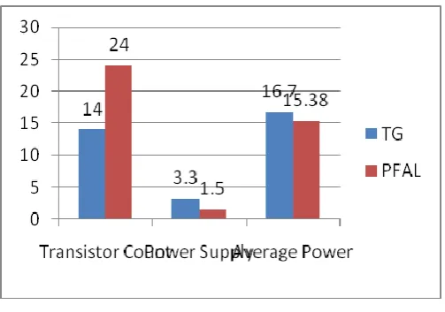
3.1Comparison of Proposed with Existing Design
The comparison between the TG and PFAL based full adder has done in various terms such as power supply, transistor count and power dissipation. The transistor count is higher in PFAL but it dissipates least energy as heat at node capacitance. In Fig.3.3 the TG and PFAL logics are compared as TG has average power of 16.7µw with proposed design power of only 15.38µw.
Table1. Table shows the Comparison between Existing and Proposed Full Adder
IV. CONCLUSION
The full adder using adiabatic logic such as PFAL compared with the TG (transmission gate) against the parameter variation. The result verified that the adiabatic full adder shows the better power result against all the parametric variation as compare to TG full adder. At high frequency the PFAL based full adder shows better power saving as compare to TG. The full adder has wide range of application like ALU, DSPs etc; adiabatic full adder can be used in any application.
REFERENCES
[1] Anjali Sharma,Richa Singh, Power efficient design of multiplexer based compressor using adiabatic logic,International Journal of Computer Applications(IJCA),Volume 81,Issue No.10 ,pp:45-50,November-2013.
[2] David John Willingham, Asynchrobatic logic for low-power VLSI design, doctoral Thesis, University of Westminster,England.UK, March,2010.
[3] Meenakhi Mishra, Shyam Akashe,High Performance ,Low power 200Gb/s 4:1 MUX with TGL in 45nm technology” AppI Nanosci(2014) 4:271-277,DOI 10.1007/s13204-013-0206-0,Springer.
[4] Abhishek Dixit, Saurabh Khandelwal, Design low power high performance 8:1 MUX using transmission gate logic (TGL), International Journal of Modern Engineering & Management Research, Volume 2
,Issue 2, pp:14-20, June 2014.
[5] Namrata Gupta, Designing of full adder circuits for low power, International Journal of Scientific Research
Engineering &Technology (IJSRET), Volume 2,Issue No.4,pp:215-219,July 2013.
[6] Amit Saxena, Deepti Shinghal, Comparative analysis of conventional CMOS and adiabatic logic gates,
International Journal of Electronics and Communication Engineering, Volume 4, Issue 1, pp: 39–43,
January 2014.
[7] Sansar Chand Sankhyan, Comparative study of different types of full adder, International Journal
of Engineering Research and Applications(IJERA), Volume 3, Issue No.5, pp: 1062-1064, Sep-Oct 2013.
[8] Nidhi Tiwari, Ruchi Sharma, Implementation of area and energy efficient full adder cell, IEEE International Conference on Recent Advances and Innovations in Engineering (ICRAIE-2014), Jaipur on 9-10 May, 2014
.
Parameters TG(Transmission
Gate) Proposed
Function Full Adder Full Adder
Technology (nm) 250 180
Supply
Voltage (V) 3.3 1.5
![Figure 1 Transmission gate logic [1]](https://thumb-us.123doks.com/thumbv2/123dok_us/7763975.1275682/2.595.147.440.554.695/figure-transmission-gate-logic.webp)
![Figure 2 Logic Symbol For Full Adder[7].](https://thumb-us.123doks.com/thumbv2/123dok_us/7763975.1275682/3.595.202.417.428.555/figure-logic-symbol-for-full-adder.webp)
![Figure 2.2 TG Based Full Adder [8] .](https://thumb-us.123doks.com/thumbv2/123dok_us/7763975.1275682/4.595.157.393.569.696/figure-tg-based-full-adder.webp)