Available online: https://edupediapublications.org/journals/index.php/IJR/ P a g e | 2942
Efficient Multi-Ternary Digit Multiplier Design In Cntfet
Technology Using Low-Complexity Adder Cells
Shaik kaleemullah 1 Patan Babjan2
[email protected] [email protected]2
1
PG Scholar, Dept of ECE, Sri Sai Institute of Technology And Science, Rayachoty, Kadapa, Andhra Pradesh.
2
Assistant Professor, Dept of ECE , Sri Sai Institute of Technology And Science, Rayachoty, Kadapa, Andhra Pradesh.
Abstract- As the scaling of Si MOSFET approaches towards its limiting value, new alternatives are coming up to overcome these limitations, CNTFET has been reviewed. This paper presents a multiternary digit (trit) multiplier design in Carbon Nanotube Field Effect Transistor (CNTFET) technology using unary operators of multivalued logic. The proposed structure is based on the classical Wallace multiplier and includes a novel ternary multiplexer design requiring only a small number of CNTFETs. Two ternary full-adder configurations are also proposed based on an examination of the multiplier structure. In addition, the design includes a new single trit multiplier which requires 67% less CNTFETs compared to a recent design. HSPICE simulations reveal low power-delay product for the proposed designs for different choices of drive strength.
Index Terms: Multiternary Digit Multiplier, Unary Operators, Carbon Nanotube Field Effect Transistor (CNTFET), Drive Strength, Noise Margin, Power-Delay Product.
I.INTRODUCTION
The alternative for the CMOS technology is the CNTFET. The similarity between CMOS and CNTFET in a device structure and principle
operation, we can obtain the required CMOS manufacturing and CMOS design in the CNTFET technology. Some of the important characteristics of CNT are: high ION/IOFF ratio, the unique dimension band which suppresses back scattering.
Comparing CNTFET and MOSFET, MOSFET have more scalability and less size which makes them more suitable for displacing. Due to the excellent electric properties of CNTFET, the CNTFET are attractive for the nano electronic applications. The CNT’s are high resistant to electro migration because the structure of a band is direct in which it enables the optical emission. Many of the efforts has been done to understand that how a CNT operates and how to improve the performance of transistor. All of the carbon bond atoms have well satisfied at the surface of carbon nano tube, which have a different semiconductor or oxide interface results. The carrier scattering mechanism and phonon vibration modes are little bit different in CNT which have different roles of phonon scattering in Carbon NanoTube Field Effect Transistor. For the low power demanding arithmetic circuits the CNTFET’s have low power consumption and high performance properties. The full adder cells are duplicated many times to build larger circuits.
Available online: https://edupediapublications.org/journals/index.php/IJR/ P a g e | 2943
Single walled carbon nanotubes (SWCNTs) have huge potential for applications in electronics because of both their metallic and semiconducting properties and their ability to carry high current. CNTs can carry current density of the order 10 μA/nm2, while standard metal wires have a current carrying capability of the order 10 nA/nm2. Semiconducting CNTs have been used to fabricate CNTFETs, which show promise due to their superior electrical characteristics over silicon based MOSFETs. Since the electron mean free path in SWCNTs can exceed 1 micrometer, long channel CNTFETs exhibit near-ballistic transport characteristics, resulting in high-speed devices. The first CNTFET was fabricated in 1998[1]. In the same year R. Martel et.al.[2] fabricated field-effect transistors based on individual single- and multi-wall carbon nanotubes and analyzed their performance.
II. PROPOSED CNTFET-BASED
TERNARY MULTIPLEXERA ternary multiplexer requiring only 15 CNTFETs can be realized utilizing unary operators for the select signal. The truth table for a ternary multiplexer is given by Fig. 2 (a) where S is the select signal and D0; D1 and D2 are the data lines. The control signal to the gate of the p and n -type CNTFETs is also indicated in Fig. 2 (a), where SP is the output of a
Fig. 1. CNTFET-based circuits for unary operators: (a)A2 (b)A2 (c) 1·AP
Wallace multiplier and includes a novel ternary multiplexer design migration because the
structure of a band is direct in which it enables the optical emission. Many of the efforts has been done to understand that how a CNT operates and how to improve the performance of transistor.
Fig. 2. Ternary multiplexer: (a) Truth table and (b) CNTFET-based circuit
positive ternary inverter and SN is the output of a negative ternary inverter. The CNTFET-based realization is shown in Fig. 2 (b) with the diameter settings for the CNT as indicated in section II.
It is worth noting that the select signals SP
and SN are the positive and negative ternary
inverters, each of which requires 2 CNTFETs, while S2 requires 3 CNTFETs (as shown in Fig. 1). The three transmission gates together require 6
CNTFETs. Further, can be generated using a negative ternary inverter with S2 as input and therefore requires 2 CNTFETs. Hence, 15 CNTFETs are required altogether.
III. PROPOSED CNTFET-BASED SINGLE-TRIT MULTIPLIER
Available online: https://edupediapublications.org/journals/index.php/IJR/ P a g e | 2944
where 1 · corresponds to min(1;
). Also, B0; B1 and B2 correspond to B = 0; 1 and 2 respectively. As a result, we obtain the ternary multiplexer-based circuit in Fig. 3 (b). The complexity is expressed by Proposition 1. Proposition 1: A single-trit multiplier can be realized with 26 CNTFETs.
Proof: Equations (1) and (2) can be realized using two ternary multiplexers whose inputs, namely 1 · AP and A2, require 9 CNTFETs (see Fig. 1 (b) and
(c)). Further, the select signal B for carry and product, requires 9 CNTFETs while 8 CNTFETs are required for the internal logic of the two multiplexers. The complete circuit is shown in Fig. 3 (c). The overall CNTFET requirement is therefore 26. Q.E.D
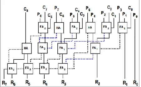
IV. PROPOSED CNTFET-BASED MULTI-TRIT MULTIPLIER
The proposed multiplier is based on the classical Wallace tree structure . The multiplier includes ternary half-adders and two custom full-adder configurations, named FA1 and FA2 which
are modifications of the traditional ternary full adder. More details are presented in section IV-B.
A. Proposed Ternary Half Adder
The truth table for a ternary half adder is the same as the one in [6]. However, one can obtain an improved circuit realization by the following observation: the sum and carry of the ternary half-adder can be expressed via unary operators as given by Equations (3) and (4). These lead to the CNTFET-based circuit in Fig. 5. The complexity of the CNTFET-realization is expressed by Proposition 2.
Proposition 2: The proposed ternary half-adder requires 35 CNTFETs.
Proof : Equations (3) and (4) can be realized by two multiplexers (one each for sum and carry) which require 21 CNTFETs altogether while the inputs to the multiplexers require 14 CNTFETs
(A1, A2, (1· ) and (1· ) require 3, 3, 2 and 2 CNTFETs respectively while AP and AN
require 2 CNTFETs each). Hence, the ternary half-adder is realized using 35 CNTFETs. Q.E.D
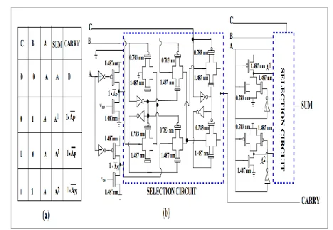
B. Modified Full Adders
The motivation for developing special full-adder configurations is as follows. The inputs to a traditional ternary full-adder have three logic levels namely, 0, 1 and 2. However, the carry output of the proposed single-trit multiplier is restricted to 0 or 1. Further, the Wallace-like structure of the proposed multitrit multiplier requires only Pi + Pj + Ck and Pi + Cj + Ck (see also Fig. 4) where Pi and Pj are product outputs of the multiplier while Cj and Ck are the carry outputs. The proposed modified full-adder FA1
computes Pi + Pj + Ck, while FA2 computes Pi +
Cj + Ck. We present the design of FA2 here. The
design of FA1 is similar. The unary operator-based
truth table for FA2 is given by Fig. 6 (a). In
Available online: https://edupediapublications.org/journals/index.php/IJR/ P a g e | 2945
Fig. 3. Proposed single-trit multiplier:(a) Truth table (P:product and C:carry) (b) multiplexer diagram and (c) CNTFET-based realization
Fig. 4. Block diagram of the proposed multi-trit (3-trit) multiplier.
Fig. 5. CNTFET-based realization of the proposed ternary half-adder
and carry outputs are given by Equations (5) and (6). In both these equations, we have two levels of ternary multiplexers (one with select line B and the other with select line C). Proposition 3 presents the transistor count for FA2.
Proposition 3: FA2 requires only 46 CNTFETs.
Proof : From Equations (5) and (6), we note that the sum and carry outputs need two MUXes each with select signal B and one MUX with select signal C. Altogether, the 6 MUXes require 32 CNTFETs (each MUX requires 4 CNTFETs while 8 CNTFETs are required for the control signals as shown in the selection circuit in Fig. 6 (b)). Realization of the data inputs requires 14 CNTFETs. Therefore, FA2 requires a total of 46
CNTFETs. Q.E.D.
C. Combining FA-1, FA-2 and Half-Adder Designs
Available online: https://edupediapublications.org/journals/index.php/IJR/ P a g e | 2946
Fig. 6. Full-adder FA2: (a) Truth table and (b) CNTFET-based realization
Proposition 4: The 3-trit multiplier requires 884 CNTFETs.
Proof : Each single-trit multiplier requires 26 CNTFETs while FA1, FA2 and the half-adder take 59, 46 and 35 CNTFETs respectively. Hence, the single-trit multipliers together take 234 CNTFETs while the adders take 650 CNTFETs. Therefore, the proposed design is realized with 884 CNTFETs. Q.E.D.
EXTENSION METHOD
Power gating technique is used to reduce the leakage power, where a sleep transistor is connected between actual ground rail and circuit ground. Low leakage 1 bit PFAL(positive feedback adiabatic logic) full adder cells are proposed for mobile applications. This will enhance the battery power by reducing the heat leakage power using PFAL Logic. By using this Adiabatic logic circuit we are reducing the power by nearly 25% than the adders of Ground Bounce techniques shown in the paper the simulations are done using DSCH & Microwind Software. Ground bounce noise is being estimated when the circuits are connected with a sleep transistor. Further, the peak of ground bounce noise is
achieved as an extension novel technique for this paper.
IV. SIMULATION RESULT
Results of proposed method
SCHEMATIC:
Layout Design:
Available online: https://edupediapublications.org/journals/index.php/IJR/ P a g e | 2947 Results of Extension method
SCHEMATIC:
Layout Design:
SIMULATION RESULT:
IV. CONCLUSION
A low CNTFET-count multiternary digit multiplier is presented. Two custom full-adder configurations are also developed. Simulations reveal excellent performance with respect to power, delay .
REFERENCES
[1] S. J. Tans, A. R. M. Verschueren, and C. Dekker, “Room-temperature transistor based on a single carbon nanotube,” Nature, vol. 393, pp. 49– 52, May 1998.
[2] A. Batchtold, P. Hadley, T. Nakanishi, and C. Dekker, “Logic circuits with carbon nanotube transistors,” Science, vol. 294, pp. 1317–1320, 2001.
[3] A. Raychowdhury and K. Roy, “Carbon Nanotube electronics: Design of high-performance and low-power digital circuits,” IEEE Trans. on Circuits Syst. I, Reg. Papers, vol. 54, no. 11, pp. 2391–2401, 2007.
[4] K. Navi, M. Rashtian, A. Khatir, and P. Keshavarzian, “High speed capacitor-inverter based carbon nanotube full adder,” Nanoscale Res. Lett., vol. 5, pp. 859–862, 2010.
[5] M. Ben-Jamaa, K. Mohanram, and G. D. Micheli, “An efficient gate library for ambipolar CNTFET logic,” IEEE Trans. Comput.-Aided Design Integr. Circuits Syst., vol. 30, no. 2, pp. 242–255, Feb. 2011.
Available online: https://edupediapublications.org/journals/index.php/IJR/ P a g e | 2948
circuits,” IEEE Trans. Nanotechnol., vol. 10, no. 2, pp. 217–225, Mar. 2011.
[7] A. Raychowdhury and K. Roy, “Carbon-Nanotube-based voltage-mode multiple-valued logic design,” IEEE Trans. Nanotechnol., vol. 4, no. 2, pp. 168–179, 2005.
[8] M. Moaiyeri, R. Mirzaee, K. Navi, and O. Hashemipour, “Efficient CNTFET-based ternary full adder cells for nanoelectronics,” NanoMicro Lett., vol. 3, no. 1, pp. 43–50, 2011.
[9] P. Keshavarzian and R. Sarikhani, “A novel CNTFET-based ternary full adder,” Circuits, Syst. Signal Process., vol. 33, pp. 665–679, 2014. [10] M. Moaiyeri, A. Doostaregan, and K. Navi, “Design of energy-efficient and robust ternary circuits for nanotechnology,” IET Circuits, Devices, Syst., vol. 5, no. 4, pp. 285–296, 2011. [11] C. S. Wallace, “A suggestion for a fast multiplier,” IEEE Trans. Electron. Comput., pp. 14–17, Feb. 1964.
[12] D. Miller and M. Thornton, Multiple Valued Logic: Concepts and Representations. Morgan Claypool, 2008.
[13] J. Deng and H. S. P. Wong, “A compact SPICE model for Carbon Nano tube Field-Effect Transistors including non idealities and its application - Part I: Model of the intrinsic channel region,” IEEE Trans. Electron Devices, vol. 54, no. 12, pp. 3186–3194, Dec. 2007.
[14] J.W.Mintmire and C.T.White, “Universal density of states for carbon nanotubes,” Phys. Rev. Lett., vol. 81, no. 12, pp. 2506–2509, 1998. [15] H. Mouftah and I. Jordan, “Design of ternary COS/MOS memory and sequential circuits,” IEEE Trans. Comput., pp. 281–288, Mar. 1977.
[16] S. Karmakar, J. Chandy, and F. Jain, “Design of ternary logic combinational circuits based on quantum dot gate FETs,” IEEE Trans. VLSI Syst., vol. 21, no. 5, pp. 793–806, 2013.
[17] D. Mateo and A. Rubio, “Design and implementation of a 5 x 5 trits multiplier in a quasi-adiabatic ternary CMOS logic,” IEEE J.