MARIYATUL QIBTHIYAH BT MOHD NOOR
A project report submitted in partial
fulfillment of the requirements for the award of the degree of Master of Engineering (Electrical - Electronics and Telecommunications)
Faculty of Electrical Engineering Universiti Teknologi Malaysia
ACKNOWLEDGEMENT
First of all, I would like to express my sincere appreciation to my project supervisor, Associate Professor Dr Mazlina Esa for encouragement, guidance, motivation and friendship.
I would also like to acknowledge my husband who gives me fully support and believe in me to do my master degree. Thank you also to my family for the never-ending support since my childhood.
ABSTRACT
On-chip radio frequency (RF) capacitor is one of the key components for RF integrated circuit (RFIC) designs such as filters and oscillators. Several researches on the design of on-chip planar capacitor have been reported. However there is a need to modify the existing synthesizing procedure; model and optimize the on-chip RF capacitor. Quality factor is the essential parameter as it is an index for the efficiency of a capacitor’s performance. This thesis investigates the design of an interdigital capacitor configuration. Geometry design variables include number of fingers, finger length, finger width, finger gap, end gap, terminal width, strip thickness, substrate height, metal types and dielectric constant. The physical model of an interdigital capacitor was
ABSTRAK
Kapasitor frekuensi radio (RF) adalah satu daripada komponen utama
rekabentuk litar bersepadu RF (RFIC ) seperti penapis dan pengayun. Beberapa kajian berkaitan rekabentuk kapasitor sesatah atas cip telah dilaporkan. Walau bagaimanapun, terdapat keperluan untuk mengubah prosedur sintesis; permodelan dan pengoptimuman kapasitor RF atas cip. Faktor kualiti adalah parameter penting sebagai indeks kecekapan pretasi pemuat. Tesis ini mengkaji rekabentuk/konfigurasi kapasitor interdigital.
TABLE OF CONTENTS
CHAPTER TITLE PAGE
TITLE i
CERTIFICATION ii
DEDICATION iii
ACKNOWLEGEMENT iv
ABSTRACT v
ABSTRAK vi
TABLE OF CONTENTS vii
LIST OF TABLES xi
LIST OF FIGURES xiii
LIST OF ABBREVIATIONS xvi
LIST OF SYMBOLS xviii
LIST OF APPENDICES xxii
1 Introduction 1
1.1 Objective 2
1.2 Scope 2
1.5 Application of Interdigital Capacitor in RFIC 4 1.6 Thesis Organization 7
2 Capacitor 8
2.1 Introduction 8
2.2 Characteristics of Capacitor 8 2.3 Types of Capacitor 10 2.4 On chip Interdigital Capacitor 14
3 Characterization of Interdigital Capacitor 16
3.1 Introduction 16
3.2 Physical Model 17
3.3 Quality Factor 19 3.4 Series Resistance 21 3.5 Capacitance Calculations 22 3.5.1 Gary D.Alley [8] 23 3.5.2 Reza Esfandiari [9] 25 3.5.3 Mohsen Naghed [14] 27 3.5.4 Farsyid Aryanfar [13] 30 3.5.5 Casares-Miranda [2] 31
3.6 Impedances 34
3.7 Mathematical Calculation Flow 37
4 Model Extraction and Electromagnetic Simulation 39 4.1 Model Extraction 39
4.2 Sub-sectioning 40 4.3 Losses in Sonnet 44 4.3.1 Metallzation Loss 44 4.2.3 Dielectric Loss 47
4.4 Q Factor 48
4.6 Design Methodology 50 4.6.1 Design Flow 51
4.6.2 ABS 52
4.6.3 De-embedding 53
5 Analysis of Interdigital Capacitor on Silicon 56
5.1 Introduction 56
5.2 Mathematical Analysis 57 5.3 Basic Design of Interdigital Capacitor 60 5.4 Effects on Quality factor and Capacitance 64 5.4.1 Design Comparison 64 5.4.2 Number of Fingers 69
5.4.3 Finger Length 72
5.4.4 Types of Metal 75
6 Conclusions and Recommendations 78
6.1 Conclusions 78
6.2 Recommendations for Future Work 80
REFERENCES 81
APPENDIX 84
APPENDIX A: MathCAD computation 84 APPENDIX B: Example of de-embedded S-parameter results 85
of the designed interdigital capacitor in Figure 5.4 (a) (0.1GHz to 9.9GHz)
APPENDIX D: Example of P-Spice format results of the 93 designed interdigital capacitor in Figure 5.4(a)
(0.1GHz to 9.9GHz)
LIST OF TABLES
TABLE NO. TITLE PAGE
2.1 Relative permittivity of insulators used in CMOS technologies 10 2.2 Summary of the properties of capacitor 12 3.1 Summarized result for Alley’s calculation 24 3.2 Interdigital capacitor geometrical parameters for Mohsen’s
experiment 29
3.3 Calculate and measured capacitances from Mohsen’s experiment 29 3.4 Model parameters of an interdigital capacitor 30 3.5 Parameter value for the interdigital capacitor 32 4.1 Properties of commonly used metals 47 5.1 Suitable combination values for finger width and number
of fingers 58
5.2 Suitable combination values for finger spacing and number
of fingers 59
5.3 Suitable combination values for number of finger and finger
length 60
5.4 Detail design geometries of the interdigital capacitors 63 5.5 Detail design parameters of Design 1 64 5.6 Qmax and C value of different design based on Figures 5.5 to 5.7 65
5.7 Qmax and C value of different number of fingers based on
5.8 Qmax and C values for different finger lengths based on Figures 5.15
and 5.16 73
5.9 Qmax and C values of different types of metal based on Figure 5.17
LIST OF FIGURES
FIGURE NO. TITLE PAGE
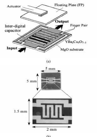
1.1 An interdigital capacitor geometry 3 1.2 A mechanically tunable superconducting microwave filter
based on interdigital capacitor: (a) the view showing a frame format of a mechanical tuning method on interdigital capacitor, (b) photograph of the pre-production interdigital
capacitor 5
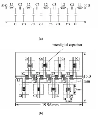
1.3 3 poles Chebyshev band pass filter of center frequency 6 GHz: (a) an equivalent circuit structure, (b) layout of the lumped
elements band pass filter 6 2.1 Print capacitors: (a) series gap in the center conductor
(b) equivalent circuit of the series gap (c) interdigital configuration (d) end-coupled overlay (e) end coupled overlay with discrete tuning elements (f) low impedance
microstrip section 13 2.2 An interdigital capacitor (a) 3D view (b) equivalent circuit model 15 3.1 An interdigital capacitor (a) side view (b) top view 17 3.2 An equivalent circuit for interdigital capacitor 18 3.3 The interdigital capacitor and its subcomponents 19 3.4 Finger capacitance contributions as a function of substrate
3.5 Finger capacitance contributions as a function of substrate
thickness 26
3.6 Quality factors from Reza Esfandiari 27 3.7 An equivalent circuit of interdigital capacitor 27
3.8 The circuit model of an interdigital capacitor in Farshid
Aryanfar’s experiment 30 3.9 Circuit model of the (a) interdigital capacitor (b) wire bonded
interdigital capacitor 33 3.10 Simulated Ceff of the IDC and WBIDC 34
3.11 TOP VIEW LAYOUT OF AN INTERDIGITAL CAPACITOR 37
3.12 Flow chart shows mathematical calculation flow 38 4.1 Illustration of the concept of subsections which affected the
memory space and processing time 41 4.2 Illustration showing the default sub-sectioning values 42 4.3 Illustration of an example of subsections view for a designed
interdigital capacitor 43 4.4 Sonnet loss model 44 4.5 Current flow around the edge of metal 45 4.6 Flow chart shows the main process in designing interdigital
capacitor by using EM software 52 4.7 Circuit designs are analyzed with the DUT in order to obtain
analysis results 54
4.8 An example of response data generated by the designed
interdigital capacitor 55 5.1 Finger width versus number of finger when finger length and
finger spacing are fixed 58 5.2 Finger spacing versus number of finger when finger length
and finger width are fixed 60 5.4(a) Design 1 of interdigital capacitor 61 5.4(b) Design 2 of interdigital capacitor 61 5.4(c) Design 3 of interdigital capacitor 62 5.4(d) Design 4 of interdigital capacitor 62 5.4(e) Design 5 of interdigital capacitor 63 5.5 S11 results for different designs of interdigital capacitor 66 5.6 S2results for different designs of interdigital capacitor 66 5.7 Effect on capacitance value, C for different designs 67 5.8 Effect on Qmax for different design of interdigital capacitor 67
5.9 Enlargement of effect on Qmax of all designs 68
5.10 Enlargement of effect on capacitance, C value for design 1
from 2 to 5 GHz 68 5.11 Enlargement of effect on Qmax for design 1 from 2 to 5 GHz 69
5.12 Effect on capacitance, C value for different number of fingers 70 5.13 Effect on Qmax for different number of fingers 71
5.14 Enlargement of effect on Qmax for different number of fingers 71
5.15 Effect on capacitance, C value for different number of fingers 74 5.16 Effect on Qmax for different finger lengths 74
LIST OF ABBREVIATIONS
ABS : Adaptive Band Synthesis AL : ALUMINUM
Bi-CMOS : Bipolar Complementary Metal Oxide Silicon C : Capacitor
CAD : Computer-aided design Cu : Copper
CMOS : Complementary Metal Oxide Silicon dB : Decibel
DC : Direct Current DUT : Device under test
ESR : Equivalent series resistance EM : Electromagnetic simulation F : Farad
FFT : Fast Fourier Transform GaAs : Gallium Arsenide GHz : Giga-hertz GND ; Ground H : Henry
HF : High frequency Hz : Hertz
Im : Imaginary KHz : Kilo-hertz L : Inductor nH : nano Henry Max : Maximum MHz : Mega-hertz
MIC : Microwave integrated circuit MIM : Metal insulator metal
Min : Minimum
MMIC : Monolithic microwave integrated circuit MOS : Metal-oxide-semiconductor
MOSFET : Metal-oxide-semiconductor-field effect-transistor PIP : Poly-insulator-poly
PF : pico Farad R : Resistor Re : Real
RF : Radio frequency
RFIC : Radio frequency integrated circuit SI : Standard International
Si : Silicon
SiO2 : Silicon oxide
Si3N4 : Silicon Nitride
S-parameter : Scattering parameter
SPICE : General purpose circuit simulation program SRF : Self-resonant frequency
TEM : Transverse electromagnetic Vs. : Versus
WBIDC : Wire bonded interdigital capacitor 2D : Two dimension
LIST OF SYMBOLS
A : Plate area
A1 : Interior capacitance of the finger
A2 : Two exterior capacitance of the finger
C : Capacitance
Ceff : Effective capacitance
Cg : Static capacitance
Cp : Parallel capacitance
Cp1 : The equivalent capacitances of gap discontinuous (port 1)
Cp2 : The equivalent capacitances of gap discontinuous (port 2)
CTE : Even mode capacitance
CTO : Odd mode capacitance
Cp : Parallel capacitance
C1 : Parasitic capacitance
C2 : Parasitic capacitance d : Separation between the plates E : Electric field
f : Frequency G : Conductance ge : Finger end gap
l : Finger length lT : Length of terminal strip
LTE : Even mode inductance
LTO : Odd mode inductance
n : Number of fingers P# : Port number
Q : Quality factor
Qc : Quality factor due to conductor losses Qd : Quality factor due to dielectric losses
Qmax : Maximum quality factor
q1total : Total charge on the inner conductor (port 1)
q2total : Total charge on the inner conductor (port 2)
q1’ : Charge per unit length on the connected transmission
lines (port1)
q2’ : Charge per unit length on the connected transmission
lines (port2) R : Resistance RDC : DC resistance
RRF : Skin effect coefficient
Rs : Series resistance
RT : Resistance of the conductors
s : Finger spacing
S11 : Input reflection coefficients
S12 : Reverse transmission coefficients
S21 : Forward transmission coefficients
S22 : Output reflection coefficients
t : Strip thickness Vin : Input voltage
Vo : Peak voltage across the circuit terminal
Vout : Output voltage
x : Finger width
Y11 : Admittance seen looking into port 1 when port 2 is short-circuit
Y12 : Transfer admittance when port 1 is short-circuit
Y21 : Transfer admittance when port 2 is short-circuit
Y22 : Admittance seen looking into port 2 when port 1 is short-circuit
Zin : Input impedance
Zc : Characteristic impedance for series configuration
Zs : Characteristic impedance for shunt configuration
Zoo : Even mode impedance
Zoe : Odd mode impedance
ZT : Characteristic impedance
Z11 : Impedance at 1 when port 2 is open
Z12 : Transition impedance when port 1 is short-circuit
Z21 : Transition impedance when port 2 is short-circuit
Z22 : Impedance at 2 when port 1 is open
DF : Attenuation constant for series configuration
DV : Attenuation constant for shunt configuration
² : Metal resistivity at DC
G : Metal skin depth
µ : Permeability
µ0 : Free space permeability
µr : Relative magnetic permeability
H : Real part of dielectric permittivity
Hc : Relative dielectric constant for series configuration
Hr : Relative dielectric constant
Ho : Free space dielectric constant
Hs : Relative dielectric constant for shunt configuration
JTE : Even mode propagation constant
JTO : Odd mode propagation constant
Ko : Free space impedance
: : Unit of resistivity, ohm
Z : Ȧ radian frequency, rad/s
I : Magnetic flux V : Bulk conductivity
S : 22/7
1.1 Objective
The objective of this research is to model and design an optimized RF interdigital capacitor for Radio Frequency Integrated Circuit (RFIC) application.
1.2 Scope
The scopes of the research are as follows:
Determination of the physical model of an interdigital capacitor and its equivalent lumped circuit
Usage of MathCAD software for mathematical configuration Determine the optimum capacitance of the capacitor
Simulation of the physical layout of the capacitor using SONNET simulation software
Analyzing the performance of the designed interdigital capacitor Thesis writing
The design specification is as follows:
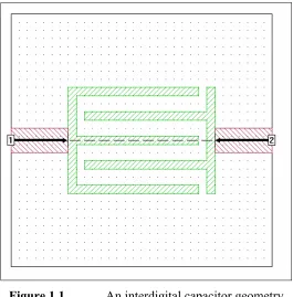
Figure 1.1 shows as example of the design geometry.
Figure 1.1 An interdigital capacitor geometry
1.3 Problem Statement
In CMOS applications, RFICs are developing a strong presence in the
commercial world. The advantages of RF CMOS technology are low cost, low power consumption, small in size, high integration, high reliability and high volume
1.4 Project Background
This project investigates the design of an interdigital capacitor. Geometry design variables include number of fingers (n), finger length (l), finger width (x), finger gap (s), end gap (ge), terminal width (wt), strip thickness (t), substrate height (h), metal types
and dielectric constant. The optimum design of an interdigital capacitor can be identified through contour plot of the quality factor (Q-factor). This project involves mathematical computation using MathCad and electromagnetic simulation using SonnetLite Plus. This optimum design of an interdigital capacitor can be used for RF applications such as filter and oscillator. Microstrip interdigital capacitors (IDCs) have been widely used as a quasi-lumped element in high frequency and high-speed
integrated circuits (ICs). [8]
Capacitors have become ubiquitous in analog-integrated circuits particularly owing to the switched capacitor technique for realization of analog-to-digital and digital-to-analog data converters and discrete time filters.
1.5 Application of Interdigital Capacitor in RFIC
Figure 1.2 and Figure 1.3 shows a mechanically tunable superconducting microwave filter based on interdigital capacitor an interdigital capacitor bandpass filter, respectively.
(a)
(b)
(a)
interdigital capacitor
(b)
1.6 Thesis Organization
REFERENCES
1. T.Ytterdal,Y.Cheng,T.A.Fjeldly, Device Modeling for Analog and RF CMOS Circuit Design. Wiley 2003
2. F.P.Casares-Miranda, P.Otero, E.Marquez-Segura, C.Camacho-Penalosa ”Wire Bonded Interdigital Capacitor,” IEEE Trans Microwave and Wireless
Components,Vol.15,No.10,2005
3. S.Hontsu,S.Mine,H.Nishikawa,M.Nakamori,A.Fujimaki,M.Inoue,A.Maehara, T.Kawai,”Study of Mechanically Tunable Superconducting Microwave Filter Using Lumped Elements,” IEEE Trans.on Applied Superconductivity
Vol3,No.2,2003
4. Leo G.Maloratsky, Passive RF & Microwave Integrated Circuits.Elsevier 2004 5. R.Brown”RF/Microwave Hybrids:Basics,Materials and Processes,” Kluwer
Academic Publishers 2002
6. W.F.Mullin, ABC’s of Capacitors, Howard W.Sams & Co 1966 7. Ian Sinclair, Passive Components for Circuit Design, Newnes 2001
8. Gary.D.Alley,”Interdigital Capacitor and Their Application to Lumped-Element Microwave Integrated Circuits”,IEEE Trans. Microwave Theory Tech,Vol MTT-18 1970
9. R.Esfandiari, D.W.Maki,M.Siracusa,”Design of Interdigital Capacitor and Their Application to GaAs Filters”, IEEE Trans. Microwave Theory Tech,Vol MTT-31 1983
11. E.Pattenhaul,H.Kapusta,A.Wisgerber,H.Mempe,J.Luginsland,I.Wolff, “CAD Models of Lumped Elements on GaAs up to 18GHz”, IEEE Trans. Microwave Theory Tech,Vol MTT-36 1988
12. M.Naghed, I.Wolff,”Equivalent Capacitances of Coplanar Waveguide Discontinuities and Interdigital Capacitors Using a Three Dimensional Finite Difference Method,” IEEE Trans. Microwave Theory Tech,Vol 38 No.12,1990 13. F.Aryanfar,K.Sarabandi’”Characterization of Semilumped CPW Elements for
Millimeter-Wave Filter Design,” IEEE Trans. Microwave Theory Tech Vol 53, No. 4,2005
14. Inder Bahl, Prakash Bhartia, Microwave Solid State Circuit Design.Wiley 2003 15. A.Naderi,M.Sawan,Y.Savaria,” A 1mW 2GHz Q Enhanced LC Bandpass Filter for Low Power RF Applications,” IEEE Trans. Microwave Theory Tech,2005 16. L.Zhu,K.Wu,”Accurate Circuit Model of Interdigital Capacitor and Its
Application to Design of New Quasi Lumped Miniturized Filters with Suppression of Harmonic Resonance,” IEEE Trans. Microwave Theory Tech,Vol 48, No3,2000
17. J.Zhou,M.J.Lancaster,F.Huang,”Superconducting Microstrip Filters Using Compact Resonators with Double-Spiral Inductors and Interdigital
Capacitors,” IEEE Trans. Microwave Theory Tech,2003
18. L.Zhu,K.Wu,”A General Purpose Circuit Model of Interdigital Capacitor for Accurate Design of Low Loss Microstrip Circuit,” IEEE Trans. Microwave Theory Tech,1998
19. S.S.Gevorgian,T.Martinsson,Peter L,J.Linner,E.L.Kollberg,”CAD Models for Multilayered Substrate Interdigital Capacitors,” IEEE Trans. Microwave Theory Tech,Vol 44 No.6,1998
20. K.Chang,Inder Bahl,Vijay Nair, RF and Microwave Circuit and Component Design for Wireless Systems. Wiley 2002
22. R.S.Chen,X.Zhang,K.F.Tsang,K.N.Yung,”Modeling and Design of Interdigital Capacitor Based on Neural Networks and Genetic Algorithm,” Microwave and Optical Technology Letters Vol.38,No.3,2003


