Abstract
TRACY, KIERAN MARK. Deposition and Electrical, Chemical and Microstructural Characterization of the Interface Formed between Pt, Au and Ag Rectifying Contacts and Cleaned n-type GaN (0001) Surfaces. (Under the direction of Robert F. Davis)
The characteristics of clean n-type GaN surfaces and the interface between this surface
and Pt, Au and Ag, have been investigated. Gallium-terminated (0001) surfaces of GaN, free of
carbon and oxygen within the detection limits of XPS have been achieved by annealing in
ammonia at 860°C for 15 minutes. Additional, in-situ surface analysis indicated a flat,
stoichometric, and unreconstructed surface free of other contaminants. The electron affinity of
this surface was 3.1 ± 0.2 eV. The valence band maximum was located 3.0 ± 0.1 eV below the
Fermi level, indicating the presence of a surface state near the valence band maximum.
Individual layers of Pt, Au or Ag were deposited in-situ on the cleaned surface and the interfaces
characterized using XPS, UPS, LEED and TEM. All as-deposited metal/GaN interfaces were
abrupt and unreacted; the Pt and Au were deposited epitaxially. The Schottky barrier heights
obtained from photoemission measurements were 1.2, 0.9 and 0.5 ± 0.2 eV for Pt, Au and Ag,
respectively. Values of the metal work function from UPS results were 5.7, 5.3 and 4.4 ± 0.2 eV
for Pt, Au and Ag, respectively. Schottky barrier heights determined via ex-situ current-voltage
measurements were 1.15, 0.88 and 0.56 ± 0.05 eV for Pt, Au and Ag, respectively.
Capacitance-voltage measurements yielded barrier heights of 1.25 and 0.96 ± 0.05 eV, for Pt and Au,
respectively. These results indicate that the Fermi level of the cleaned surface is not pinned.
Upon annealing the aforementioned contacts from 400 to 800°C for 3 minutes each. The
rectifying behavior of the Pt and Au contacts degraded as a function of temperature during
annealing at 400, 600 and 800°C for 3 minutes each until they became ohmic. This was correlated
with TEM of the annealed interfaces, which displayed increased chemical reaction and
Dedicated to my parents Robert and Anita and to my brother and sister
iii Biography
Acknowledgements
Graduate school was such a great challenge that I could not have succeeded without the support and help of my family, friends and colleagues. Not only have I developed and grown as a scientist/engineer, I have grown as a person during the past five years, from this experience.
First I would like to thank Dr. Robert Davis for his continued support, encouragement and patience during this endeavor and for the opportunity to work as part of his research group. His guidance as a scientist, mentor and friend is greatly appreciated. I would also like to thank Dr. Robert Nemanich his enthusiasm and guidance in this research and the opportunity to work with him and his team of researchers. I feel very luck to have been able to work with two outstanding research groups during my graduate career. I would also like to thank Dr. Zlatko Sitar and Dr. Robert Kolbas for serving as members of my committee and as mentors.
The next two people I would like to thank are Cecilia Upchurch and Jan Jackson. They are the keystones to the Nemanich and Davis research groups, respectively. Without them keeping things on track there would be a state complete chaos in the research groups. Cecilia and Jan, thank you very much for your friendship, assistance and just for listening.
For years the PAMS shop has been able to make the equipment designs in created in the lab a reality. This was no small task given the complexity of the designs and the naivety of the designers. For that I am very grateful to artisans in the shop: Frank Milkowski, Mike Gregory, Hai Bui, Tim Harvell, and Lynn Smith. I would also like to thank Steve Jenkins in the physics electronic shop for his assistance.
I would also like to thank Joan O’Sullivan and others in the microelectronics fabrication facility for their assistance in the processing of my samples.
I would like to thank the Office of Naval Research and the Kenan Institute for their financial support of this research.
Although I believe that thanks are not enough, I would like to thank all of my colleagues in both the Davis Research Group and the Surface Science Laboratory for your friendship and assistance.
v Ja-Hum Ku, Dr. Hoon Ham, Phillip Hartleib, Andrew Banks, Dimitri Alexson, Morgan Ware, Brian Rodriguez, Steve English, Pradeep Rajagopal, Dr. John Barnak, Dr. Mark Benjamin, Dr. Leah Bergman, Dr. Wilhelm Platow, Dr. Kenneth Järrendahl, Dr. Carsten Ronning, Dr. Eliane Maillard-Schaller. Dr. Bob Therrien, and Eric Carlson.
There are some good friends that helped me develop as a person while I was in graduate school. As such I am a better person today for having the following people as my friends: Dr. Ladye Wilkinson, Lina Cuartas-Ward, Wendy Taylor Preble, Cathy Hartman, Raphaela Platow, Eric and Lizette Watko, Bill and Kimberly Hunt, Rob and Leigh Bright, Marvin Barnett, Dan and Wendy Clinton, Matt ‘Hank’ Davis, Paul Lizio, Greg Hrycak, Greg Pontorno, and Nuvit Celikgil.
I would like to thank Nortel Networks for sponsoring the ice hockey team I played on while I was in graduate school. It was really good to get away from school and work for a while. Thanks is also expressed to the past and present members of the Nortel Red B League hockey team: Kevin Boyle, Derek Dubois, Leo Banville, Rich DiMassimo, Scott Fisher, Bob Fors, Pete Getzoff, Rich Kviring, Hobie Orton, Hobie Orton Jr, Bob Petrunka, Everett Poore, Rick Porter, Fred Redden, Jeff ‘The Hammer’ Hartman, Greg Heuss, Bob and Doug McKenzie and coach Phil McCracken.
Table of Contents
List of Tables………xii
List of Figures………..xiii
1 Introduction to GaN: Growth, Properties and Applications ... 1
1.1 Introduction... 1
1.2 Properties of Gallium Nitride ... 5
1.2.1 Growth ... 5
1.2.2 Substrates ... 6
1.2.3 Physical and Electronic Properties of GaN... 7
1.3 Outline of Dissertation... 7
2 Schottky Barriers: Formation, Modeling and Characterization Techniq... 15
2.1 Introduction... 15
2.2 Formation of Schottky Barriers ... 16
2.2.1 Basic electrical properties of Metals and Semiconductors ... 16
2.2.2 Schottky-Mott Model... 18
2.2.3 Interface/Surface State Model... 22
2.2.4 Other Models for Barrier Height Formation... 25
2.3 Characterization Techniques... 29
2.3.1 Current transport processes... 29
2.3.2 Current-Voltage Measurements (I-V)... 30
2.3.3 Capacitance-Voltage (C-V) ... 33
2.3.4 Photoemission... 35
2.3.4.1 Introduction to Photoemission ... 36
2.3.4.2 Determination of the Schottky barrier height using photoemission ... 39
2.4 Conclusions... 41
3 Equipment and Experimental Section... 57
3.1 Introduction... 57
3.2 Equipment... 57
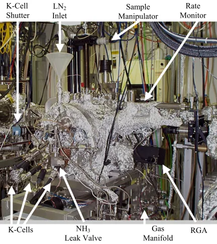
3.2.1 Integrated Surface Analysis and Growth System ... 57
3.2.2 Sample Holders and Sample Manipulation... 58
3.2.3 Sample Heaters ... 60
vii
3.2.5 Gas Source Molecular Beam Epitaxy System (GSMBE)... 66
3.2.6 Electron Beam metal evaporation system... 68
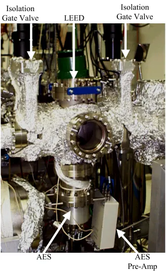
3.2.7 Auger Electron Spectroscopy (AES) and Low Energy Electron Diffraction (LEED) System ... 70
3.2.8 Angle Resolved Ultra-Violet Photoelectron Spectroscopy System (ARUPS) 71 3.2.9 Electrical Testing System and Photolithography Mask Set... 74
3.3 Experimental Procedure... 75
3.3.1 Sample Preparation and Ex-situ cleaning ... 76
3.3.2 In-Situ Processing and Characterization... 77
3.3.3 Ex-Situ Sample processing and characterization... 81
3.4 Summary... 82
4 Preparation and Characterization of atomically clean, stoichometric GaN surfaces 99 4.1 Introduction... 99
4.2 Experimental Procedures ... 100
4.2.1 Material ... 100
4.2.2 Ex-situ Preparation... 100
4.2.3 In-situ Preparation... 101
4.2.4 In-Situ Characterization ... 102
4.2.4.1 X-ray Photoelectron Spectroscopy (XPS) ... 102
4.2.4.2 Ultraviolet Photoelectron Spectroscopy (UPS) ... 103
4.2.4.3 Low Energy Electron Diffraction (LEED) ... 104
4.2.5 Ex-Situ Characterization... 104
4.2.5.1 Atomic Force Microscopy (AFM) ... 104
4.2.5.2 Transmission Electron Microscopy (TEM) ... 104
4.3 Results... 105
4.3.1 X-ray Photoelectron Spectroscopy (XPS) ... 105
4.3.2 Ultraviolet Photoelectron Spectroscopy (UPS) ... 110
4.3.3 Low Energy Electron Diffraction (LEED) ... 114
4.3.4 Atomic Force Microscopy (AFM) ... 114
4.4 Discussion... 115
4.4.1 As-loaded surface... 115
4.4.2 ‘Clean’ Surface ... 117
4.5 Conclusions... 120
5.2 Experimental Procedure... 137
5.2.1 Material ... 137
5.2.2 Ex-Situ Preparation... 137
5.2.3 In-situ processing and characterization... 138
5.2.3.1 Surface Preparation... 139
5.2.3.2 Metal depositions ... 140
5.2.3.3 X-ray Photoelectron Spectroscopy (XPS) ... 140
5.2.3.4 Ultraviolet Photoelectron Spectroscopy (UPS) ... 141
5.2.3.5 Low Energy Electron Diffraction (LEED) ... 142
5.2.4 Ex-Situ Characterization... 142
5.2.4.1 Electrical Characterization... 142
5.2.4.2 Transmission Electron Microscopy (TEM) ... 145
5.3 Results... 146
5.3.1 Surface cleaning... 146
5.3.1.1 X-ray Photoelectron Spectroscopy (XPS) ... 146
5.3.1.2 Ultraviolet Photoelectron Spectroscopy (UPS) ... 146
5.3.1.3 Low Energy Electron Diffraction (LEED) ... 147
5.3.2 Platinum-Gallium Nitride Interface ... 147
5.3.2.1 X-ray photoelectron spectroscopy (XPS) ... 147
5.3.2.2 Ultraviolet photoelectron spectroscopy (UPS) ... 154
5.3.2.3 Low Energy Electron Diffraction (LEED) ... 157
5.3.3 Ex-Situ Electrical Characteristics ... 158
5.3.3.1 As-Deposited Contacts... 158
5.3.3.2 Annealed Contacts ... 162
5.3.3.3 TEM of the unannealed and annealed interfaces ... 163
5.4 Discussion... 165
5.4.1 Surface Science Analysis of the Pt-GaN interface ... 165
5.4.1.1 Interface Chemistry and Structure ... 165
5.4.1.2 Electronic Properties... 166
5.4.2 Electrical Characterization... 168
5.4.2.1 As-deposited contacts ... 168
5.4.2.2 Annealed Contacts ... 169
5.5 Conclusions... 171
6 Properties of the Gold - clean Gallium Nitride Interface... 200
6.1 Introduction... 200
6.2 Experimental Procedure... 201
6.2.1 Material ... 201
6.2.2 Ex-Situ Processing... 201
ix
6.2.3.1 Surface Preparation... 203
6.2.3.2 Metal Depositions ... 203
6.2.3.3 X-Ray Photoelectron Spectroscopy (XPS) ... 204
6.2.3.4 Ultraviolet Photoelectron Spectroscopy (UPS) ... 205
6.2.3.5 Low Energy Electron Diffraction (LEED) ... 206
6.2.4 Ex-Situ Characterization... 206
6.2.4.1 Electrical Characterization... 206
6.2.4.2 Transmission Electron Microscopy (TEM) ... 209
6.3 Results... 210
6.3.1 Surface Cleaning... 210
6.3.2 Gold-Gallium Nitride Interface... 211
6.3.2.1 X-Ray Photoelectron Spectroscopy (XPS) ... 211
6.3.2.2 Ultraviolet Photoelectron Spectroscopy (UPS) ... 215
6.3.2.3 Low Energy Electron Diffraction (LEED) ... 217
6.3.3 Electrical Characterization... 218
6.3.3.1 As deposited contacts... 218
6.3.3.2 Annealed Contacts ... 222
6.3.3.3 TEM of the unannealed and annealed interfaces ... 223
6.4 Discussion... 225
6.4.1 Surface Analysis of the Gold-GaN Interface ... 225
6.4.1.1 Interface Chemistry and Structure ... 225
6.4.1.2 Electronic Properties... 226
6.4.2 Electrical Characterization... 227
6.4.2.1 As-Deposited Contacts... 227
6.4.2.2 Annealed Contacts ... 228
6.5 Conclusion ... 228
7 Properties of an atomically clean GaN-Silver interface... 254
7.1 Introduction... 254
7.2 Experimental Procedure... 255
7.2.1 Material ... 255
7.2.2 Ex-Situ Processing... 255
7.2.3 In-Situ Processing and Characterization... 256
7.2.3.1 Surface Preparation... 256
7.2.3.2 Metal Depositions ... 257
7.2.3.3 X-Ray Photoelectron Spectroscopy (XPS) ... 258
7.2.3.4 Ultraviolet Photoelectron Spectroscopy (UPS) ... 259
7.2.4 Ex-Situ Characterization... 259
7.2.4.1 Electrical Characterization... 259
7.3.1 Surface Cleaning... 261
7.3.1.1 X-ray Photoelectron Spectroscopy (XPS) ... 261
7.3.1.2 Ultraviolet Photoelectron Spectroscopy (UPS) ... 261
7.3.1.3 Low Energy Electron Diffraction (LEED) ... 262
7.3.2 Silver-GaN Interface... 262
7.3.2.1 X-ray Photoelectron Spectroscopy ... 262
7.3.2.2 Ultraviolet Photoelectron Spectroscopy (UPS) ... 266
7.3.2.3 Low Energy Electron Diffraction (LEED) ... 268
7.3.3 Ex-Situ Electrical Characteristics ... 269
7.3.3.1 As-Deposited Contacts... 269
7.3.3.2 Annealed Contacts ... 270
7.3.4 Discussion... 272
7.3.5 Conclusions... 274
8 Summary, Conclusions and Future Research ... 290
8.1 Introduction... 290
8.1.1 Atomically Clean GaN Surface ... 290
8.1.2 Metal-GaN Interfaces... 292
9 Recommended Future Research... 297
10 Survival Guide for SiC/GaN/AlN Processing in Dabney 28 GSMBE ... 301
10.1 Wafers: Silicon Carbide... 301
10.2 SiC Ex Situ Cleaning ... 302
10.3 SiC In situ cleaning... 304
10.3.1 Thermal desorption of oxide... 304
10.3.2 B. SiH4 Clean/CVC (Chemical Vapor Cleaning) Æ Recommended.. 305
10.4 AlN Buffer Layer Growth... 306
10.5 GaN Growth on AlN... 308
10.6 GaN-NH3 CVC Clean... 309
10.7 System Venting... 310
10.8 Pumping out the system... 312
10.9 System Bake out ... 313
10.10 Ti Filament Outgasing ... 314
11 Procedures for LEED and AES... 315
xi
11.2 AES: Auger Electron Spectroscopy... 315
11.3 DIF data file format. ... 317
12 Electron Beam Evaporation System – Dabney 28... 318
12.1 Metal Deposition... 318
12.2 Venting of the E-beam / AES-LEED System ... 320
12.3 E-Beam: Replenish/Changing of Metal Targets... 321
13 Dicing Saw Operation... 323
13.1 Wafer Prep ... 323
13.2 Dicing Saw Prep (part 1): Start up... 323
13.3 Dicing Saw Prep: Alignment ... 323
13.4 Dicing Saw Prep: Parameter Input... 324
13.5 Wafer Cutting ... 324
13.6 Removal of the wax ... 325
14 RF Sputtering System Operation (Riddick 141)... 326
14.1 Inserting sample in RF chamber ... 326
14.2 Pump down the chamber after loading the sample ... 326
14.3 Sputtering Setup... 326
14.4 Target Pre-Sputtering... 327
14.5 Move the sample under the target... 327
14.6 Removing the sample... 327
14.7 Pump down the system ... 328
List of Tables
Table 1.1 Physical properties of GaN and some other common semiconductors. Values complied from refs [1-5,10-12]... 10 Table 1.2 Electronic properties of GaN and some other common semiconductors. Values complied from refs [1-5,10-12]... 11 Table 2.1Table of metal work functions and electronegativities... 45 Table 2.2 Band Gap energies and electron affinities for some common semiconductors.45 Table 4.1 As-loaded and Clean GaN Photoemission results for a) XPS and b) UPS... 123 Table 5.1 Photoemission results summary for a) XPS and b) UPS from the platinum-GaN interface... 175 Table 6.1 Photoemission results summary for a) XPS and b) UPS from the gold-GaN
interface... 232 Table 7.1 Photoemission results summary for a) XPS and b) UPS from the silver-GaN
xiii List of Figures
Figure 1.1 Plot of band gap energy versus lattice parameter for some common semiconductors. ... 12 Figure 1.2 Illustration of the wurtzite structure looking down the basal plane (0001). The dark spheres represent the position of gallium atoms and the light spheres represent the position of nitrogen atoms... 13 Figure 1.3 Illustration of the wurtzite structure looking down the (11-20) direction. The dark spheres represent the position of gallium atoms and the light spheres represent the position of nitrogen atoms... 14 Figure 2.1 Individual Energy Band diagrams for metals and semiconductors a) φm > χs and b) φm < χs... 46 Figure 2.2 Energy band diagram for intimate metal semiconductor contacts for a) φm > χs (rectifying) and b) φm < χs (ohmic). ... 47 Figure 2.3 Energy band diagram for Interface state model ... 48 Figure 2.4 Plot of the S parameter vs. semiconductor electronegativity. From Kurtin et. al.[9] ... 49 Figure 2.5 Illustration of the various current transport mechanisms. ... 50 Figure 2.6 Energy band diagrams for a) forward biased and b) reverse biased junctions 51 Figure 2.7 Illustration of the 3-step photoemission model indicating a) initial state, b)
excitation, c) transport and d) emission of electrons from a surface. ... 52 Figure 2.8 Illustration of electron excitation from UPS and XPS. V is the valence band, Vac is the vacuum level and 2p, 2s, 1s are core level states... 53 Figure 2.9 Universal curve for electron escape depth. From Briggs and Seah.[24]... 54 Figure 2.10 Illustration for determining the a) electron affinity of a semiconductor and b) work function of a metal from UPS spectra... 55 Figure 2.11 Illustration depicting the technique used to determine the Schottky barrier
Figure 3.3 Transfer Line System Heater a) plan view and b) side view... 86 Figure 3.4 Heater calibration curve for SiC-GaN samples. ... 87 Figure 3.5 X-ray Photoelectron Spectroscopy (XPS) system... 88 Figure 3.6 XPS survey scan spectra for gold standard of a calibrated spectrometer.
Spectrum was acquired using the magnesium anode (hν=1253.6 eV) and a pass energy of 50 eV... 89 Figure 3.7 XPS core level spectrum of gold 4f peaks for a calibrated spectrometer.
Spectrum was acquired using the magnesium anode (hν=1253.6 eV) and a pass energy of 20 eV... 90 Figure 3.8 Gas-Source Molecular Beam Epitaxy (GSMBE) system... 91 Figure 3.9 Internal layout of the GSMBE with Sample holder, Doser, K-Cells and Cryo Shroud. (Not to scale). ... 92 Figure 3.10 Electron Beam metal evaporation (E-beam) system. ... 93 Figure 3.11 Internal schematic of E-beam system... 94 Figure 3.12 Low Electron Energy Diffraction (LEED) and Auger Electron Spectroscopy (AES) systems... 95 Figure 3.13 Angle Resolved Ultraviolet Photoelectron Spectroscopy (ARUPS) system. 96 Figure 3.14 Layout of the contact patterns. ... 97 Figure 3.15 Electrical testing system schematic. ... 98 Figure 4.1 X-ray photoelectron spectra for a) as-loaded GaN and b) clean GaN obtained using Mg Kα x-rays (hν=1253.6 eV) and c) as-loaded GaN and d) clean GaN obtained using Al Kα x-rays (hν=1486.6 eV). Spectrometer pass energy was set to 50 eV... 124 Figure 4.2 Gallium 2p core level XPS spectra for a) as-loaded GaN and b) clean GaN
surfaces. Spectra were obtained using a pass energy of 20 eV and Mg Kα x-rays.125 Figure 4.3 Gallium 3d core level XPS spectra for a) as-loaded GaN and b) clean GaN
surfaces. Spectra were obtained using a pass energy of 20 eV and Mg Kα x-rays. 126 Figure 4.4 Nitrogen 1s core level XPS spectra for a) as-loaded GaN and b) clean GaN
xv Figure 4.5 Oxygen 1s core level spectra for a) as-loaded GaN and b) clean GaN surfaces.
Spectra were obtained using a pass energy of 20 eV and Mg Kα x-rays. ... 128 Figure 4.6 Carbon 1s core level XPS spectra for a) as-loaded GN and b) clean GaN
surfaces. Spectra were obtained using a pass energy of 20 eV and Al Kα x-rays. 129 Figure 4.7 Ultraviolet photoelectron spectra for a) as-loaded GaN and b) clean GaN
surfaces. Spectra were obtained using He I (hν=21.2 eV) radiation at a pass energy of 10 eV... 130 Figure 4.8 Expanded views of UPS spectra obtained for a) as-loaded GaN and b) clean
GaN surfaces. Spectra were obtained using He I (hν=21.2 eV) radiation at a pass energy of 10 eV... 131 Figure 4.9 Expanded view of the valence band maximum region of the UPS spectra for a) as-loaded GaN and b) clean GaN surfaces. Spectra were obtained using He I (hν=21.2 eV) radiation at a pass energy of 10 eV. ... 132 Figure 4.10 Band diagrams for a) flat band GaN (calculated) and b) clean GaN (UPS
measurements). ... 133 Figure 4.11 Low energy electron diffraction (LEED) images obtained for a) as-loaded
GaN and b) clean GaN surfaces. Beam energy was 80 eV for both images... 134 Figure 4.12 Atomic force microscopy (AFM) scans for a) as-loaded GaN and b) clean
GaN surfaces. Measured RMS roughness values were 3 and 4Å for a) and b) respectively. ... 135 Figure 5.1 Evolution of XPS survey scan spectra for multiple platinum layers deposited on a clean GaN surface. A pass energy of 50 eV was used along with the Magnesium anode (hν=1253.6 eV) in the collection of this data... 176 Figure 5.2 Gallium 2p XPS core level spectra for multiple platinum depositions on clean gallium nitride. Spectra obtained using the magnesium anode (hν-1253.6) and a pass energy of 20 eV... 177 Figure 5.3 Gallium 3d XPS core level spectra evolution for multiple platinum depositions on clean gallium nitride. Spectra acquired using the magnesium anode (hν=1256.6 eV) and a pass energy of 20 eV. ... 178 Figure 5.4 Nitrogen 1s XPS core level spectra evolution for multiple platinum
Figure 5.5 Platinum 4f doublet XPS core level spectra for multiple platinum depositions on clean gallium nitride. Spectra acquired using the magnesium anode (hν=1253.6 eV) and a pass energy of 20 eV. ... 180 Figure 5.6 Plot of the attenuation of the gallium 3d core level peak intensity as a function of platinum layer thickness. The theoretical curves represent the three different growth modes usually observed in epitaxial growth, 2 dimensional layer-by-layer (Frank-van der Merwe) growth, mixed (Stranski-Krastanov) growth, and 3 dimensional (Volmer-Weber) growth. The SK and VW curves were generated using a coverage value of 0.5 and an initial thickness of 5 angstroms... 181 Figure 5.7 Evolution of UPS survey spectra for multiple platinum layers on clean gallium nitride. Spectra obtained using helium I radiation (hν=21.2 eV) from a discharge lamp... 182 Figure 5.8 UPS spectra of the valence band maximum region for clean gallium nitride
and GaN with platinum layers of various thicknesses. The spectra were obtained using He I radiation (hν=21.2 eV). ... 183 Figure 5.9 UPS survey spectra for clean GaN, 10 angstroms of platinum on clean GaN
and 700 angstroms of Pt on GaN. The shift in the bulk GaN feature is used to determine the position of the VBM before and after metal depositions, which can then be used to determine the Schottky barrier height of the Pt-GaN interface. The 700-angstrom layer of platinum represents 'bulk' platinum. Spectra acquired using He I radiation (hν=21.2 eV)... 184 Figure 5.10 LEED images for a) 15 angstroms of platinum deposited on clean GaN and b) 700 angstroms of platinum deposited on GaN. Beam energy for both images was 90 eV... 185 Figure 5.11 Current-Voltage plot for as-deposited 100-micron diameter platinum contacts deposited on a clean GaN surface. This plot illustrates the rectifying nature of the contact. ... 186 Figure 5.12 Semi-logarithmic plot of current-voltage data for as-deposited 100-micron
diameter Pt contacts on clean GaN. ... 187 Figure 5.13 Current-voltage data plot for as-deposited 100-micron diameter Pt contacts
on clean GaN. This figure illustrates the breakdown of the contact. The breakdown is catastrophic, after which the contact is no longer rectifying... 188 Figure 5.14 Semi-logarithmic plot of the forward current of as-deposited Pt contact on
xvii following labels a) ohmic contact, b) Schottky contact, c) 25 µm spacing, d) 100 µm diameter, e) 1.2 µm thick GaN thin film and f) 0.1 µm thick AlN buffer layer. .... 189 Figure 5.15 Plot of the capacitance versus voltage for as-deposited 100-micron diameter Pt contact on clean GaN... 190 Figure 5.16 Plot of (A/C)2 versus applied bias for as-deposited 100-micron diameter Pt contacts on clean GaN. The Schottky barrier and ionized impurity concentration can be determined from the line fit to the data points. ... 191 Figure 5.17 Plot of the doping profile for the GaN used in these experiments. This profile was obtained from the C-V data. The zero bias depletion region is approximately 800 angstroms thick. ... 192 Figure 5.18 Current-voltage characteristics for as-deposited and annealed 100-micron
diameter platinum contacts on clean GaN. The annealing temperatures were 400, 600 and 800°C for 3 minutes each... 193 Figure 5.19 Semi-logarithmic plot of the current-voltage characteristics for as-deposited and annealed 100-micron diameter Pt-GaN contacts. The annealing temperatures were 400, 600 and 800°C for 3 minutes each. ... 194 Figure 5.20 Semi-logarithmic plot of reveres bias I-V characteristics for as-deposited and annealed 100-micron diameter Pt-GaN contacts. The annealing temperatures were 400, 600 and 800°C for 3 minutes each... 195 Figure 5.21 HRTEM of the as-deposited Pt-GaN interface... 196 Figure 5.22 HRTEM image of the Pt-GaN interface after annealing at 400°C for 3
minutes... 197 Figure 5.23 HRTEM of the Pt-GaN interface after annealing at 800°C for 3 minutes.
Image a) is an overview of the interface and image b) is a close up of the interface region. ... 198 Figure 5.24 AES spectra obtained for the unannealed and annealed Pt surfaces of the
Figure 6.2 Gallium 3d XPS core level spectra evolution for multiple gold depositions on clean GaN. Spectra acquired using the magnesium anode and a pass energy of 20 eV... 234 Figure 6.3 Nitrogen 1s XPS core level spectra evolution for multiple gold depositions on clean GaN. Spectra obtained using the Mg anode and a pass energy of 20 eV... 235 Figure 6.4 Gold 4f doublet XPS core level spectra for multiple gold depositions on clean GaN. Spectra acquired using the Mg anode and a pass energy of 20 eV. ... 236 Figure 6.5 Plot of the attenuation of the gallium 3d core level peak intensity as a function of the gold layer thickness. The theoretical curves represent the three different growth modes usually observed in epitaxial growth, 2-D layer-by-layer (Frank-van der Merwe) growth, mixed (Stranski-Krastanov) growth, and 3-D (Volmer-Weber) growth. The SK and VW curves were generated using a coverage value of 0.5 and an initial thickness of 5 angstroms... 237 Figure 6.6 Evolution of the UPS survey spectra obtained for multiple gold layer
depositions on clean GaN. Spectra obtained using He I radiation from a discharge lamp... 238 Figure 6.7 UPS spectra of the valence band maximum region for clean GaN and GaN
with gold layers of various thicknesses. The spectra were obtained using He I radiation. ... 239 Figure 6.8 UPS survey spectra for clean GaN, 10 Å of gold on GaN and 750 Å of gold on GaN. The shift in the bulk GaN feature is used to determine the position of the VBM before and after metal depositions, which can then be used to determine the Schottky barrier height of the Au-GaN interface. The 750 Å thick layer of Au represents ‘bulk’ gold. Spectra acquired using He I radiation... 240 Figure 6.9 LEED images for a) 20 Å of Au deposited on clean GaN and b) 750 Å of Au deposited on clean GaN. Beam energy was 90 eV. ... 241 Figure 6.10 Semi-logarithmic current-voltage plot for as-deposited 100-micron diameter gold contacts deposited on a clean GaN surface. This plot illustrates the reverse bias leakage current and forward bias current for a rectifying contact. ... 242 Figure 6.11 Current-voltage plot for as-deposited 100-micron diameter Au contacts. The plot illustrates the catastrophic breakdown of the contact. ... 243 Figure 6.12 Semi-logarithmic plot of the forward bias current for as-deposited
xix a) ohmic contact, b) Schottky contact, c) 25 µm spacing, d) 100 µm diameter, e) 1.2 µm thick GaN thin film and f) 0.1 µm thick AlN buffer layer. ... 244 Figure 6.13 Plot of the capacitance versus voltage for as-deposited 100-micron diameter Au contacts... 245 Figure 6.14 Plot of (A/C)2 versus applied bias for as-deposited 100-micron diameter Au contacts. The Schottky barrier and ionized impurity concentration are determined from the intercept and slope, respectively. ... 246 Figure 6.15 Plot of the doping profile for the GaN used in these experiments. The
depletion region is approximately 720 Å thick... 247 Figure 6.16 Current-voltage characteristics for as-deposited and annealed 100-micron
diameter Au contacts on clean GaN. The annealing temperatures were 400, 600 and 800°C for 3 minutes each... 248 Figure 6.17 Semi-logarithmic plot of the forward bias current for as-deposited and
annealed Au contacts. Contact diameter is 100-microns. The annealing temperatures were 400, 600 and 800°C for 3 minutes each. ... 249 Figure 6.18 HRTEM images of an unannealed Au-GaN interface... 250 Figure 6.19 HRTEM images of the Au-GaN interface after annealing at 400°C for 3
minutes... 251 Figure 6.20 HRTEM images of the Au-GaN interface after annealing at 800°C for 3
minutes... 252 Figure 6.21 AES spectra of the surface of the unannealed and annealed Au-GaN samples prior to TEM samples preparation. ... 253 Figure 7.1 Evolution of XPS survey scan spectra for multiple silver layers deposited on a clean GaN surface. A pass energy of 50 eV was used along with the magnesium anode in the collection of this data... 278 Figure 7.2 Gallium 3d XPS core level spectra evolution for multiple silver depositions on clean GaN. Spectra acquired using the magnesium anode and a pass energy of 20 eV... 279 Figure 7.3 Nitrogen 1s XPS core level spectra evolution for multiple silver depositions on clean GaN. Spectra obtained using the Mg anode and a pass energy of 20 eV... 280 Figure 7.4 Silver 4d doublet XPS core level spectra for multiple silver depositions on
Figure 7.5 Plot of the attenuation of the gallium 3d core level peak intensity as a function of the silver layer thickness. The theoretical curves represent the three different growth modes usually observed in epitaxial growth, 2-D layer-by-layer (Frank-van der Merwe) growth, mixed (Stranski-Krastanov) growth, and 3-D (Volmer-Weber) growth. The SK and VW curves were generated using a coverage value of 0.7 and an initial thickness of 6 angstroms... 282 Figure 7.6 Evolution of the UPS survey spectra obtained for multiple silver layer
depositions on clean GaN. Spectra obtained using He I radiation from a discharge lamp... 283 Figure 7.7 UPS spectra of the valence band maximum region for clean GaN and GaN
with silver layers of various thicknesses. The inset plot shows the Fermi level turn-on for the various silver layer thicknesses. The spectra were obtained using He I radiation. ... 284 Figure 7.8 UPS survey spectra for clean GaN, 10 Å of silver on GaN and 750 Å of silver on GaN. The shift in the bulk GaN feature is used to determine the position of the VBM before and after metal depositions, which can then be used to determine the Schottky barrier height of the Ag-GaN interface. The 700 Å thick layer of Ag represents ‘bulk’ silver. Spectra acquired using He I radiation. ... 285 Figure 7.9 Current-voltage plot for as-deposited 100-micron diameter silver contacts
deposited on a clean GaN surface. This plot illustrates the reverse bias leakage current and forward bias current for a rectifying contact... 286 Figure 7.10 Semi-logarithmic plot of the forward bias current for as-deposited
100-micron diameter Ag contacts on clean GaN. The ideality factor and Schottky barrier height are determined from the slope and intercept of the linear region between 0.1 and 0.2 eV. The inset figure depicts the contact geometry with the following labels a) ohmic contacts, b) Schottky contact, c) 25 µm spacing, d) 100 µm contact dimensions, e) 1.2 µm thick GaN thin film and f) 0.1 µm thick AlN buffer layer. 287 Figure 7.11 Current-voltage characteristics for as-deposited and annealed 100-micron
diameter Ag contacts on clean GaN. The annealing temperatures were 400 and 600°C for 3 minutes each... 288 Figure 7.12 Semi-logarithmic plot of the forward bias current for as-deposited and
1 Introduction to GaN: Growth, Properties and Applications
1.1 Introduction
The development of microelectronics/semiconductor technology in the last 30 years can be considered on of man’s most important developments. Not only has this technology developed into one of the leading industries in the world, driving the economies of many nations, it has had an immense impact on the way people work, live and play. From computer processors to cell phones, the products created from this technology revolutionized how people live. Currently silicon technology is the oldest and most refined; however, it is not the only semiconductor technology in use today. Other semiconductors material classes such as SiGe-, GaAs- and phosphide-based semiconductors are finding applications in current devices.
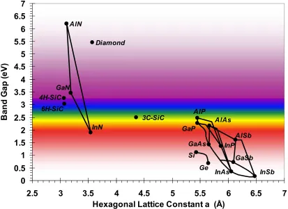
Together with AlN (Eg=6.2 eV) and InN (Eg=1.89 eV), GaN (Eg=3.4 eV) forms a group of direct band gap materials that can be used in tandem to engineer the electronic and some physical properties of a semiconductor around a specific device design, rather than designing a device around a semiconductor. For instance, the GaN-InN system has already had a significant impact regarding the commercial development and sales of optoelectronic devices including Light Emitting Diodes (LED’s), Laser Diodes (LD’s) and photo-detectors. By alloying InN and GaN to form InxGa1-xN, the band gap of the resulting InGaN can possibly be engineered between 1.89 to 3.4 eV, which is the energy range for infrared, visible, and ultraviolet light. Potentially the LED’s fabricated from these materials would be able to emit light in any color of the visible spectrum. Thus, one material class can be used for all LED applications, which could reduce processing costs.
The GaN-AlN material system is being extensively investigated for applications for high-power, high-frequency and high-temperature microelectronic devices including field effect transistors (FET’s). Alloying GaN with AlN to form AlxGa1-xN, semiconductors with band gaps ranging from 3.4 to 6.2 eV can be fabricated. As in the case of the InGaN, the Ga to Al ratio in the material controls the band gap energy. This flexibility and applicability in the materials are what engineers and scientists are trying to exploit for future applications. Figure 1.1 displays a plot of the lattice parameters and band gaps for a number of semiconductor material systems.
3 universities to address the challenges of developing GaN-based devices. Materials issues from the growth, properties and dynamics of GaN thin films to actual device fabrication and characterization are specifically being addressed. One area of study is the research of the basic properties of metal-semiconductor interfaces as they form one foundation from which all present and future device applications are and will be based.
the substrate material. These contacts are usually described as rectifying contacts with the magnitude of the barrier being very small. The concept of barrier height is discussed in detail in Chapter 2.
Rectifying contacts are of particular interest because of their current blocking properties. As such, these contacts have applications as gate contacts in photo-detectors, high-power diodes and a many of transistors designs. Transistors fabricated using Schottky contacts as gates are easy to fabricate and the resulting devices can have higher switching speeds because they do not rely on minority carriers to generate the active regions of the device, as is the case for p-n junctions and MOS devices.
For the great potential of GaN-based semiconductors to be realized, some important research must be conducted regarding the properties of its surface and the properties of metal-GaN interfaces. In this study, the electrical, chemical and microstructural properties of both an atomically clean GaN surface and metal-semiconductor interfaces for the clean GaN have been extensively investigated.
5
1.2 Properties of Gallium Nitride
1.2.1 Growth
The growth of GaN dates to the early 1940’s when ammonia was passed over hot gallium. The result was GaN needles. [4] Small poly-crystals were produced through most of the 1960’s. While this material was useful for basic studies of its physical and electronic properties, it was insufficient for device fabrication and further materials characterization. The vapor phase growth of single crystal GaN thin films were reported by Maruska and Tietjen in 1969. [6] These authors used HCl as the transport gas to carry the gallium into the system and ammonia as the nitrogen source for growth on a sapphire substrates. The resulting films were highly n-type. Acceptor-type GaN was mentioned; however, they reported that it was difficult to reproduce. Their work grew out of the techniques used to fabricate other III-V semiconductors such as GaAs and GaP. Subsequently, GaN was grown as thin crystalline films on various substrates using vapor phase epitaxy. The next advance involving the growth of GaN occurred when Yoshida et al.[7] Amano et al.[8,9] introduced an AlN buffer layer using MBE and MOVEP, respectively. This lead to a substantial increase in GaN related research in film growth and device development. Techniques for growing p-type GaN were discovered by Amano and Akasaki[9] using Mg as the acceptor impurity.
1.2.2 Substrates
Since large area bulk single crystal GaN is not available, this compound and related nitrides must be grown on foreign substrates. The physical properties of the substrate, including crystal structure, lattice spacing, thermal expansion and electrical conductivity should match as closely as possible to the thin film being grown. Hexagonal, wurtzite GaN is most commonly grown on sapphire and silicon carbide substrates. Figure 1.2 and Figure 1.3 are images of the (0001) and (11-20) directions in a wurtzite lattice.
Sapphire (Al2O3), an insulator, is the most common substrate, because it is readily available as single crystal wafers. Sapphire possesses a hexagonal, corundum crystal structure. The atomic spacing in the (0001) plane are not close to that of GaN. The lattice mismatch between the GaN and sapphire at the closest distance is about 15%, which is very large. The lattice mismatch is the difference between the lattice parameters of the two materials. This can be related to the amount of stress in the films. The sapphire is transparent because of its large band gap, which makes it useful for optical applications where light is needed to pass through the substrate. The cost of sapphire wafers is much less as compared to the other popular substrate for GaN growth, silicon carbide.
7 GaN and 6H-SiC is about 3%. Silicon carbide can also be doped n and p-type; thus, it is possible that vertical devices can be fabricated on GaN grown on SiC, unlike the case for sapphire. The use of SiC as a substrate will most likely occur for high-power, high frequency and high-temperature devices.
1.2.3 Physical and Electronic Properties of GaN
Table 1.1 and 1.2, contain some of the basic physical and electronic properties of GaN and provides a comparison with Si and GaAs. Physical properties including thermal conductivity, lattice parameters, and density are listed in Table 1.1. Electronic properties including the band gap energy, dielectric constant, mobility and effective mass are tabulated in Table 1.2.
1.3 Outline of Dissertation
Chapter 2 contains discussions of Schottky barrier height formation and characterization techniques. The Schottky-Mott model, interface dipole model and other models used to explain barrier height formation are discussed. Characterization techniques such as photoemission, current-voltage and capacitance-voltage are also covered.
Chapter 4 details the experiments and results of characterization of the as-loaded and ammonia cleaned GaN surfaces. The chemical, electronic and physical properties of the surface are discussed.
Chapter 5 describes the experimental details and results of the formation of the platinum-GaN interface on atomically clean GaN surfaces. The chemical, electrical and physical properties of the interface are covered. Formation of the Schottky barrier is investigated using various in-situ and ex-situ techniques.
Chapter 6 describes the experimental details and results of the formation of the gold-GaN interface on atomically clean GaN surfaces. The chemical, electrical and physical properties of the interface are covered. Formation of the Schottky barrier is investigated using various in-situ and ex-situ techniques.
Chapter 7 describes the experimental details and results of the formation of the silver-GaN interface on atomically clean GaN surfaces. The chemical, electrical and physical properties of the interface are covered. Formation of the Schottky barrier is investigated using various in-situ and ex-situ techniques.
9 References
1 S. C. Jain, M. Willander, J. Narayan, and R. V. Overstraeten, Journal of Applied Physics 87, 965 (2000).
2 S. J. Pearton, J. C. Zolper, R. J. Shul, and F. Ren, Journal of Applied Physics 86, 1-78 (1999).
3 B. Monemar, Journal of Materials Science: Materials in Electronics 10, 227-54 (1999).
4 J. I. Pankove and T. D. Moustakas, in Gallium Nitride (GaN) I; Vol. 50, edited by J. I. Pankove and T. D. Moustakas (Academic Press, San Diego, 1998), p. 517. 5 J. H. Edgar, S. Strite, I.Akasaki, H.Amano, and C. Wetzel, Properties, processing
and applications of Gallium Nitride and Related Semiconductors, Vol. 23 (IEE Books, 1999).
6 H. P. Maruska and J. J. Tietjen, Applied Physics Letters 15, 327-329 (1969). 7 S. Yoshida, S. Misawa, and S. Gonda, Applied Physics Letters 42, 427-9 (1983). 8 H. Amano, I. Akasaki, K. Hiramatsu, N. Koide, and N. Sawaki, Thin Solid Films
163, 415-20 (1988).
9 H. Amano, I. Akasaki, T. Kozawa, K. Hiramatsu, N. Sawak, K. Ikeda, and Y. Ishi, Journal of Luminescence 40-41, 121 (1988).
10 S. M. Sze, Physics of Semiconductor Devices, Second Edition ed. (John Wiley & Sons, New York, 1981).
11 S. Strite and H. Morkoc, Journal of Vacuum Science & Technology B (Microelectronics Processing and Phenomena) 10, 1237-66 (1992).
Table 1.1 Physical properties of GaN and some other common semiconductors. Values complied from refs [1-5,10-12].
Physical
Properties GaN AlN InN 6H-SiC Si GaAs Sapphire
Crystal
Structure Wurtzite Wurtzite Wurtzite Wurtzite Diamond Zincblende Corundum
Lattice
Constants a (Å) 3.189 3.112 3.548 3.081 5.431 5.653 4.758
c (Å) 5.185 4.982 5.760 15.117 --- --- 12.99
Thermal Conductivity
(W/cmK)
1.3-1.7 2.0 0.45-0.8 3.0-3.8 1.5 0.46 0.46
Thermal Expansion ∆a/a
(10-6/K)
5.59 4.2 3.6 4.2 2.6 6.9 9.2
Thermal Expansion ∆c/c
(10-6/K)
3.17 5.3 2.6 4 --- --- 9.3
Melting Temp
(°C) >1700 3000 1100 2830 1414 1238 2050
Density (g/cm) 6.15 3.23 6.81 3.21 2.33 5.32 3.98
Index of
11
Table 1.2 Electronic properties of GaN and some other common semiconductors. Values complied from refs [1-5,10-12].
Electrical
Properties GaN AlN InN 6H-SiC Si GaAs
Band Gap
Energy (eV) 3.4 6.2 1.89 3.03 1.12 1.42
Band Gap
Transition Direct Direct Direct Indirect Indirect Indirect Dielectric
Constant εr 9.5 8.5 15.3 9.66 11.9 13.1
Dielectric
Constant ε∞ 5.35 4.77 8.4 6.7 ---
---Electron Effective Mass
me (mo)
0.22 0.33 0.11 0.45 0.98 0.067
Hole Effective
Mass mh (mo) 0.8 --- --- 1.2 0.49 0.45
Electron Mobility
µe (cm2/Vs) 900 300 4400 500 1500 8500
Hole Mobility µh
(cm2/Vs) 15 14 --- 50 450 400
Sat. Drift Velocity (107cm/s)
2.5 --- 2.5 2.0 1.0 2.0
Breakdown
Figure 1.1 Plot of band gap energy versus lattice parameter for some common semiconductors. 0 0.5 1 1.5 2 2.5 3 3.5 4 4.5 5 5.5 6 6.5 7
2.5 3 3.5 4 4.5 5 5.5 6 6.5 7
Hexagonal Lattice Constant a (Å)
13
2
Schottky Barriers
: Formation, Modeling and
Characterization Techniq
2.1 Introduction
Metal-Semiconductor contacts act as bridges between microelectronic devices and the macroscopic world of applications. The two basic types of contacts are Ohmic and Schottky or rectifying. The dynamics of current flow between the metal and the semiconductor are a determining factor in the type of contact. Symmetric current flow for positive and negative biasing of the contact is a hallmark of Ohmic contacts; while an asymmetric current flow, under the same conditions is characteristic of Schottky or rectifying contacts. The properties of the metal and the semiconductor have been related to the various types of contacts, with each type having specific applications. For example, Ohmic contacts are used to supply current for devices (source and drain contacts). Meanwhile, Schottky contacts are mainly used to block current flow (diode and gate contacts).
2.2 Formation of Schottky Barriers
2.2.1 Basic electrical properties of Metals and Semiconductors
Before a discussion of the electronic structure of metal-semiconductor interfaces can be initiated, the basic electronic properties of metals and semiconductors must be addresses individually. Topics such as conduction band, valence band, band gap, Fermi level, work function, and electron affinity are discussed individually for metals and semiconductors. The following discussions will be restricted to n-type semiconductors only; however, the extension to p-type semiconductors can be easily achieved.
The band diagram of a metal is depicted in Figure 2.1 (a and b). As noted above, the energy bands of a metal tend to have overlapping energy bands resulting in the absence of a band gap. This is usually described by stating that the conduction band minimum is at or below the valence band maximum of the metal. A metal is usually defined in terms of a Fermi level (Efm) or Fermi energy and a work function (φm). The Fermi level is that energy at which there is a probability of ½ for a state at that level to be occupied by an electron. For metals, the Fermi level can also be described as the highest occupied state.[1,2] The work function of the metal is the difference in energy between the vacuum level and the Fermi level. Where the vacuum level is the bottom of the free electron band. For most metals the value of the work function is in the range of 3.0 eV to 5.5 eV.[3] Table 2.1 contains the values of work functions for some common metals.
In contrast to metals, semiconductors have a more complicated band structure. Semiconductors have a conduction and valence band separated by the band gap, as depicted in Figure 2.1(a&b). At room temperature, approximately 300K, the conduction band of an intrinsic (undoped) semiconductor is usually sparsely populated with electrons while the valence band is essentially filled. As in the case of the metal, a Fermi level can be defined for a semiconductor (Efsc). However, the Fermi level in the latter is not in a fixed position, rather it can be positioned throughout the band gap by the introduction of dopants or impurities.
the Fermi level is dependant on the doping, the work function of the semiconductor also depends on the doping and can have a large range of values. Thus, the work function of a semiconductor does not accurately describe the energy relations of the bands to the vacuum energy. This can lead to problems with defining the electronic properties of the material.
A more appropriate quantity is the electron affinity of the semiconductor (χs). The electron affinity is defined as the energy difference between the vacuum level and the conduction band minimum. This value is effectively independent of the Fermi level position and thus, independent of the semiconductor doping. The electron affinity for some common semiconductors is given in Table 2.2. Figure 2.1 depicts the independent band structures for a metal and a semiconductor for the situation in which a) the work function of the metal is greater than the electron affinity of the semiconductor and b) the electron affinity of the semiconductor is larger than work function of the metal.
The next few sections deal with the case when metals and semiconductors are placed in contact with each other. Some general models, which try and predict the formation of Schottky barriers, will be presented.
2.2.2 Schottky-Mott Model
function and the electron affinity of the semiconductor according to the following equation.
s m b φ χ
φ = − (2.1)
Where φm is the metal work function and χs is the electron affinity of the semiconductor. From equation 2.1, the barrier height of different metals on a semiconductor should vary linearly with the work function of the metal. Accordingly, there are two cases that can arise. Case one arises when the metal work function is greater than the semiconductor electron affinity, (φm>χsc). This is the case that leads to the energy barrier formation and rectifying behavior of the metal-semiconductor contacts. The second case occurs when the work function is less than the electron affinity, (φm<χsc), which leads to an Ohmic contact. However, case II is rarely observed in the laboratory, since most metal-semiconductor contacts result in the formation of a barrier.
the concentration of donor electrons in the semiconductor is much less than that of the electrons in the metal, the electrons that flow from the semiconductor to the metal originate from a surface and a sub surface region of the semiconductor that are collectively referred to as the depletion region.[4]
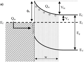
Charge neutrality of the system dictates that the negative charge, Qm, on the metal surface is offset by the positive charge in the depletion region of the semiconductor Qsc.[5] As a result of the charge build up, an electric field is formed in the depletion region of the semiconductor. This field causes the Fermi levels to align, resulting in the bands of the semiconductor to bend at the interface. For an n-type semiconductor, the bands bend upwards. This bending of the energy bands resulting from the alignment of the Fermi levels produce the potential barrier, φb, at the metal-semiconductor interface, as depicted in Figure 2.2(a).
From Figure 2.2(a), φb is the resulting barrier height, Vbi is the built in potential, w is the depletion width, Qsc is the semiconductor charge and Qm is the charge at the metal surface. The built in voltage can be expressed as the difference between the work functions of the two materials.
s m bi
qV =φ −φ (2.2)
The built in voltage can also be referred to as the contact potential and is a measure of the band bending at the semiconductor surface.
enough energy to overcome the full barrier height, φb. On the other hand, electrons in the semiconductor see a potential barrier of qVbi. Electrons can flow from the semiconductor to the metal if Vbi can be overcome. Current flow when positive and negative biases are applied is asymmetric and similar to that of a p-n junction. This will be discussed further in another section on the electrical characterization of contacts.
Case II occurs when the work function of the metal is less than the electron affinity of the semiconductor. The energy bands line up according to the diagram in Figure 2.2(b). In this instance, when the metal and semiconductor are placed in intimate contact electrons are transferred from the metal surface into the semiconductor. When the electrons are transferred to the semiconductor, the Fermi level is raised to coincide with the Fermi level of the metal. As a result, the conduction and valence bands bend downward. Once equilibrium is achieved, a positive charge is built up on the metal surface and a negative charge built up in the surface and sub-surface regions of the semiconductor. This accumulation region of electrons in the semiconductor is due to the downward bending of the bands to at the interface. The resulting Schottky barrier height for this type of contact is negative. Current can flow in either direction without being blocked by potential barriers. Unfortunately, contacts of this type are very rare. Most metal-semiconductor contacts are of type I.
2.2.3 Interface/Surface State Model
Unfortunately when actual metal-semiconductor contacts are investigated, the results did not correlate to predictions of the Schottky-Mott model. Studies have shown that for covalently bonded semiconductors; such as silicon, and germanium, there is a weak dependence between metal work function and barrier height. Bardeen[6] in 1947 was first to propose a model to explain this behavior. The presence of interface states in the band gap of the semiconductor was the central argument of this model. He proposed that these states were responsible for the deviation of actual contacts from the Schottky-Mott model. Since that time, further research has determined that surface states can also be present in the band gap of a semiconductor. As such, the terms “interface state” and “surface state” have been used interchangeably.
These states are energy levels that reside in the classically forbidden band gap of the semiconductor. These states can be due to the termination of the periodic lattice (dangling bonds), surface defects in the lattice and/or contamination and impurities at the semiconductor surface. These states can be either continuous through the entire band gap or exist as discrete levels in the gap.[6]
when empty, they behave as donors.[7] There is a charge transfer between the bulk of the semiconductor and the surface states. A negative charge is built up in the surface states while a positive charge builds up in the semiconductor. A depletion region in the semiconductor forms from the formation of a dipole at the surface of the semiconductor. As a result of the depletion region, upward band bending occurs for an n-type semiconductor. This is contrary to the description of an isolated semiconductor used in the Schottky-Mott model, as shown in Figure 2.1(a&b).
The presence of these states affects the properties of metal-semiconductor contacts. The surface states screen the semiconductor from the metal. For a high density of surface states, the work function of the metal has no effect on the depletion region. Thus, the Schottky barrier forms due to the interaction of the surface states and the bulk of the semiconductor and can be expressed as
o g b E φ
φ = − (2.3)
Figure 2.3 illustrates the band diagram for the interface/surface state model. From Figure 2.3; φb is the barrier height, Qss is the charge on the surface states, φo is the neutral level, δ is the thickness of the depletion layer, ∆V is the drop in potential across the depletion layer, and the other terms were defined in previous sections.
n o
g m
b γ φ χ γ E φ φ
φ = ⋅( − )+(1− )( − )−∆ (2.4)
s i i D eδ ε ε γ +
= (2.5)
where φo is the neutral level, δ is the interface thickness, Ds is the density of surface states, ∆φn in the image force lowering, εi is the dielectric constant for the interface layer, and the other terms have been defined previously.
Image force lowering is a reduction of the barrier height due to the electric field generated from a moving electron in the semiconductor.[4] The effect on the barrier height is generally small since the value is not large; approximately a couple of meV. However, it can have an effect on the current transport process across the barrier.
From equations 2.4 and 2.5, three distinct cases arise for the Schottky barrier height. In the first case, the density of surface states, Ds is zero; subsequently δ approaches unity. The barrier height is completely dependant upon the work function of the metal.
n sc m
b φ χ φ
φ = − −∆ (2.6)
This is the Schottky-Mott model of the metal-semiconductor junctions with a correction for image force lowering, and represents an upper limit to the barrier height. The slope of the plot of barrier height versus work function yields a value of unity.
barrier height in now defined in terms of the semiconductor band gap and the neutral level according to the following equation.
n o g
b E φ φ
φ = − −∆ (2.7)
In this case the plot of barrier height versus work function has a slope approaching zero. Finally, when the density of surface states is low there are insufficient states in the gap to adsorb the charge transfer between the metal and the semiconductor. Therefore, the resulting barrier is in part due to the difference between the metal work function and the semiconductor electron affinity. As result, the slope of the barrier height versus the work function resides in the range between zero and unity.
2.2.4 Other Models for Barrier Height Formation
and metal states[17,18]. The following is a brief discussion intended to introduce some of the other methods used in explaining the formation of Schottky barriers.
A model involving the ionicity of the metal and semiconductor was proposed by Kurtin et.al.[9] The electronegativity or bond ionicity of the semiconductor plays a large role in the determination whether or not the Fermi level is pinned. They defined a slope parameter S from the plot of the barrier height versus metal electronegativity.
m b
dX d
S= φ (2.8)
Freeouf and Woodall[10] proposed a model for barrier formation based on metal-semiconductor interface reactions. The model put fourth by these investigators is a refinement of the Schottky-Mott model where an interface reaction between the metal and semiconductor is responsible for the subsequent barrier height. This model postulates that the Fermi level is not pinned by surface states. The barrier formation is related to the work function of micro-clusters, which result from the metal reacting with surface contamination or the semiconductor during the metal deposition process. Accordingly, the work function of the metal from equation 2.1 is replaced with an effective work function (φeff). This effective work function is an average of the work functions of the different phases present at the metal-semiconductor interface, but mainly due to the work function of the anion.[10]
Tersoff[14,19] introduced the concept of interface dipoles to explain the MIGS model of barrier height formation. He stated that changes in the interface dipole were created when a metal-semiconductor interface is formed, created the MIGS and was responsible for the band shifting in the semiconductor. These shifts in the band can then be used to explain the formation of the Schottky barrier height.
Spicer et al.,[15,16] developed an alternate MIGS model, which is called the unified defect model. Their model relates the induced states to defects formed at the metal semiconductor interface during interface formation. These defect levels are then used to explain the pinning of the Fermi level. This model was developed from the fact that some carefully prepared semiconductor surfaces did not display any initial pinning. After the introduction of the metal adatoms, Fermi level pinning was observed. They attributed this behavior to the creation of structural defects on the semiconductor surface by the metal adatoms.
2.3 Characterization Techniques
Unlike the modeling of Schottky barriers the measurement and characterization techniques of such barriers are rather well known and accepted. Electrical characterization involves the measurement of the current or capacitance for applied voltages and will be discussed in the following sections. Photoemission is another technique that has been employed in the past few decades to measure the Schottky barrier height. The benefit of photoemission is that the formation of the metal-semiconductor interface can be investigated non-destructively. Its use has increased due to the proliferation of UHV equipment in the research laboratory as a result of better vacuum systems and techniques and lower equipment costs that have occurred in the last 20 years. Photoemission will be briefly discussed in section 2.3.4.1. In section 2.3.4.2 the discussion will change to the measurement of the barrier height.
This section is intended to introduce the topics of metal-semiconductor interface characterization. For more in-depth discussions the reader is directed towards the following references.[4,5,20-22]
2.3.1 Current transport processes
transport processes. For most moderately doped semiconductors, thermionic emission is dominant over the others. By contrast, for heavily doped semiconductors, tunneling currents can dominate. One of the principal materials engineering techniques employed in the formation of Ohmic contacts is it over doping of the semiconductor to achieve tunneling currents. The direction of the current flow depends on the polarity of the voltage, and will be discussed in the next section.
2.3.2 Current-Voltage Measurements (I-V)
The current-voltage technique involves the application of a range of biases (positive and negative) to the metal-semiconductor system and the measurement of the resulting current.
The band diagram shown in Figure 2.2(a) represents a typical rectifying metal-semiconductor contact at equilibrium without any bias applied. The net current flow in this situation is zero. The current flowing from the semiconductor to the metal is offset by an equal and opposite current flow from the metal to the semiconductor.
and the current flow from the metal to the semiconductor is greater than the opposing current (remember current flow is in the opposite direction to electron flow).
Reverse (negative) DC biasing of the semiconductor with respect to the metal results in the Fermi level of the semiconductor being lowered with respect to the metal. The lowering of the semiconductor Fermi level increases the band bending in the semiconductor, as shown in Figure 2.6(b). The barrier for electrons in the semiconductor (Vbi) is increased as a result of the increased band bending. As in the positive bias case, the barrier for electron flow from the metal to the semiconductor (φb) is again unchanged. In this situation, the electron flow from the semiconductor to the metal is decreased. Thus, the net current flow is then from the semiconductor to the metal.
Characteristics of a good rectifying contact are that the forward bias current is many orders of magnitude greater than the reverse bias current. For low values of the forward bias, small increases in the bias should cause the current to substantially increases until a limit is reached and the current flow linearly increases. Resistance of the material is responsible for the linear increase of the current for large forward biases. Meanwhile, for changes in the reveres bias, the resulting current flow should not appreciably change.
Most Schottky contacts are fabricated on moderately doped semiconductors thus thermionic emission over the barrier is usually assumed. Sze[5], discussed the derivation of the equations of thermionic emission by Bethe. This theory yields an equation that explains the current density for ideal metal semiconductor contacts.
− −
= * 2exp exp 1
kT qV kT q T A
where φb is the Schottky barrier height, q is the electronic charge, k is Boltzman’s constant, T is the temperature and A* is Richardson’s constant. The current density (J) is the current divided by the area of the contact.
For practical rectifying metal semiconductor contacts the above equation is usually modified to the following[4]
− − = kT qV nkT qV J
J oexp 1 exp (2.10)
− = kT q T A J b
o * 2exp φ (2.11)
where n is the ideality factor and all the other quantities were defined above. The ideality factor is a number that represents the contacts deviation from the ideal situation. With the assumption that V is greater than 3kT/q, equation 2.10 can be simplified to
= nkT qV J
J oexp (2.12)
When measuring metal semiconductor contacts, the current not the current density, is normally measured. Thus equation (1.10) becomes
= nkT qV I
I oexp (2.13)
− = kT q T AA I b o φ exp 2
* (2.14)
where A is the contact area and the other terms have been previously defined.
above 3kT, there should be a linear region that extends over many decades of the current for very small changes in applied current. By using a linear extrapolation of the data to V=0, Io can be determined from the current axis intercept. By solving equation 1.14 for φb as a function of Io, the Schottky barrier height can be determined by substituting Io in
to the following equation.
= o b I T AA q
kT * 2
ln
φ (2.15)
The value of the Richardson constant yields the largest uncertainty in the calculation of φb. However, since it appears in the logarithm term an error in A* by a factor of two only
yields a difference in φb of less than a tenth of an electron volt.[22]
The ideality factor of the diode can be determined from the slope of the linear extrapolation using slope kT q n ⋅
= (2.16)
In general, ideal diodes have ideality factors in the range 1.02 < n < 1.1. Deviation of n from this range can be caused my many different factors such as, a thick interface layer or recombination in the depletion region.[4]
2.3.3 Capacitance-Voltage (C-V)
DC signal. As a result of the application of the signal, charges of opposite sign are induced on the semiconductor and metal surfaces. This change in charge gives rise to a junction capacitance. The metal-semiconductor interface can be regarded as a parallel plate capacitor with the depletion region acting as the separation between the electrodes. Applying a range of reverse biases to the contact and measuring the resulting capacitances form the basis for these measurements. Rhoderick and Williams[4,5], and Sze[5] discuss the derivation of the capacitance of the metal-semiconductor junction.
The depletion region width can be expressed by the following equation
− − = q kT V V qN W bi d o scε ε 2 (2.17)
Where Vbi is the built in voltage, V is the applied reveres bias, Nd is the donor concentration, εo is the permittivity of vacuum, and εsc is the semiconductor dielectric constant. The charge of the depletion region is given as
− − = = q kT V V N q W qN
Qsc d 2 εscεo d bi (2.18)
The capacitance can then be expressed as
− − = ≡ q kT V V A N q V Q C bi d o sc sc 2 2 ε ε δ δ (2.19)
Equation 2.19 can be rewritten as
All the variables in equation 2.20 are constant except the applied bias (V); therefore, the plot of 1/C2 versus V should be linear.
Thus, capacitance voltage data is generally presented as plots of A2/C2 versus voltage.[22] Linear extrapolation is performed on the data with the slope being
(
q sc oNd)
slope
ε ε
2
= (2.21)
Accordingly the carrier concentration can be determined from the slope of the extrapolation. The intercept on the voltage axis Vi can be used to determine the barrier height as follows
kT V qVi o
b = − +
φ (2.22)
Where Vo is the difference between the conduction band minimum and Fermi level. The value of φb obtained from this method is for flat band conditions.
In general, the value of φb(C-V) is greater than φb(I-V), since current-voltage measurements are more sensitive to the defects and imperfections at the metal-semiconductor interface. Current-Voltage (I-V) measurements are more sensitive to non-uniformity of the interface than C-V measurements. Capacitance-voltage (C-V) measurements are sensitive to defects in the gap of the semiconductor.
2.3.4 Photoemission