Volume 3, Issue 4, April 2014
Page 305
Abstract
A low power current stimulator with high accuracy for electrical stimulation has been presented. Programmable constant current is generated making use of a simple voltage to current converter. In order to thwart the non-idealities, which cause errors in the output current value, a Low power SAR Analog to Digital Converter (ADC) is employed to act as part of a digital feedback loop. It monitors the state of stimulator and updates the output of Digital to Analog Converter (DAC) according to the difference between the desired and actual value. To have a safe stimulation a charge balancing technique has been employed with reduced high voltage (HV) switches. In order to elevate the efficiency, based on the value of DAC, dynamic power supply technique can be used. The idea was implemented via low-power, low-area Off-The-Shelf components. It is designed to deliver charge balanced biphasic current pulses with scopes corresponding to the one which is used in Deep Brain Stimulation (DBS). The circuit was tested in Saline (0.9% NaCl) for in vitro tests.
Keywords: Charge balancing, deep brain stimulation (DBS), digital feedback loop, programmable constant current, voltage to current converter.
1. Introduction
During the past decade, the development of implantable electrical stimulators has had a great role in treatment of neuronal disabilities such as deep brain stimulation, cochlear implant, and retinal implant [1], [2]. Their conventional approach is to deliver programmed electrical pulses through the electrode(s). The pulses are trimmed to excite or inhibit the action potential adjacent to the nervous tissues. There are two general types of stimulation namely voltage and current stimulation. In voltage stimulations the voltage pulses with specific pulse durations and frequencies are delivered to the tissue. By selecting the supply voltage near to the output voltage, the efficiency could be improved [3], [4]. However, due to changes in the impedance of the electrode-tissue, the exact stimulation current and charge is not controllable. However, in current stimulators, the current and charge that is injected to the tissue is precisely manipulated. Therefore, regardless of the impedance changes at the electrode-tissue interface, constant current stimulation causes the desired neural excitations. Although, in current stimulators the power dissipation is more than its voltage mode counterparts and thus the efficiency will degrade drastically [5]. In the proposed stimulator the power consumption of the current stimulator is decreased by eliminating the operational amplifier (OPAMP), in addition the efficiency can be simultaneously increased. Another important issue in stimulators is electrode dissolution or tissue destruction caused by the remaining voltage at the end of stimulation in electrode-tissue interface. In order to prevent tissue damage, stimulation waveforms must be biphasic which consists of cathodic phase followed by an anodic phase. During the cathodic phase the cell membrane will be depolarized. Then the anodic phase compensates the charge injected through cathodic phase. As a general rule in charge balanced stimulation, the voltage across the electrode must stay within a safe window [6], [7]. Some charge balancing methods which use a passive or active approach have been introduced. In the proposed circuit a passive charge equalizer is used so that the remaining voltage at the end of the cathodic and anodic phases would be negligible, without using any excess switches.
The organization of this paper is as follows: in section 2 a literature survey on the previously proposed current stimulators has been done. In section 3 the concept of the proposed current stimulator circuit is explained. It is demonstrated that the proposed circuit also benefits from the precise current stimulation, besides decreasing the power consumption. Finally, the proposed circuit is simulated, implemented and practically tested and the results are shown in section IV.
2. Literature Review
In order to generate programmed current pulses, the most straightforward way is to use a current DAC. However in some other works a voltage mode DAC followed by a voltage to current converter is used. Both approaches are discussed in this section.
Current mirroring DAC employs binary weighted size transistors which mirror a reference current according to the input digital codes [8]. The current mirror works until all transistors are kept in the saturation region. To consume less voltage headroom and elevate the accuracy of mirroring, the size of the transistors should be increased at the expense of larger area consumption. In [9], transistor sizes are kept equal and their biases are binary weighted voltages. One drawback of
A High Precision, Low Power Programmable
Current Stimulator for Safe Neural Stimulation
Farhad Bozorgi1, Reza Ranjandish2, Sina Ghanbari3 and Omid Shoaei4
1, 2, 3
Department of Electrical and Computer Engineering, University of Tehran, Tehran, Iran
4
Volume 3, Issue 4, April 2014
Page 306
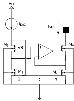
these stimulators is their low output resistance which may cause variation at the output currents. To overcome this issue a wide swing cascade configuration is used in order to boost the output resistance and current accuracy as shown in Figure 1 [10]. The output impedance (
r
out) is boosted by :4 4 2
out ds ds
r
Agm r r
(1)+
-VB
M2 M1
M3 M4
IStim IDAC
VDD
1 : n
Figure 11. Wide swing cascade current mirror with boosted output resistance.
where A is the gain of the amplifier, gm4 is transconductance of M4, rds4, rds2 are the drain to source resistances of M4 and
M2 respectively. IDAC branch dissipates static power equal to scaled output currents. In order to circumvent such a waste in
power, the current DAC has been put in series with the output stage.
The current stimulators shown in Figure 2 are based on a voltage follower. In Fig 2(a) the programmed voltage produced by the voltage mode DAC is placed on the resistor through a voltage follower. The OPAMP and transistor (M1) close the feedback loop. The DAC voltage across resistor produces the desired current with a boosted output resistance [11]. To consume less voltage headroom, in Figure 2(b) a small fixed voltage is set on the drain-source of M1 (Vref), in a manner
that it pushes it into the triode region [12]. It works as a voltage control resistor where the gate bias voltage is produced with a DAC (VDAC). The generated output current (IStim) is :
1
1
( )
stim ox DAC T Ref
W
I C V V V
L
(2)
where VT is threshold voltage, µ is the mobility, Cox is gate oxide unit capacitance, and W1 , L1 are the width and length of
the transistor M1. This system has linearity problems due to the second effects of the transistors and to overcome this
problem in Figure 2(c) the binary weighted transistors are employed. All of them work in triode region and they are controlled with logic gate voltages of “0” or “1” according to the output current [13].
The static power consumption wasted by these stimulators is the drawback. For example the OPAMP has a quiescent current that is wasting power even during non-stimulus phase. The supply voltages in these stimulators are constant, therefore efficiency degrades. A solution to this problem was proposed in [14] where a flexible power supply is used to conserve the voltage headroom in different output currents and load impedance.
Another type of current stimulator works on the concept of current copying structure [15]. As shown in Figure 3 it operates in two phases. In the storage phase (S1), the desired current (Iin) passes through M1 and CMEM stores the
equivalent gate voltage generated on M1, at the same time its drain to source voltage is set in a way that it operates in the
triode region. In the stimulation phase (S2), the same drain voltage is still held on M1 and regarding to the voltage stored
on CMEM , without the need for active circuit, the stimulation current is generated. However the leakage current is a
problem here since it may change the output current value and therefore CMEM must be updated frequently.
Volume 3, Issue 4, April 2014
Page 307
Figure 13. Stimulator based on current copying DAC.
3. Proposed Current Stimulator
The presented stimulator works based on a voltage mode DAC and a new precision current to voltage converter in a way that the OPAMP would not be needed. As it was mentioned the current pulses should be biphasic in order to equalize the charge. The biphasic structure with charge balancing that uses the proposed current stimulator is introduced. In order to elevate the efficiency, this system is capable of providing control signals for dynamic supply voltage.
3.1 Proposed current generator
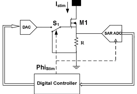
The presented current generator uses an NMOS as a simple nonlinear voltage to current converter. As it can be seen in Figure 4 by using a digital calibration, the required voltage can settle across the resistor R to generate the defined stimulation current. Hence, the method of regulating is important. The raw method is to use a lookup table which has the gate-source voltage of M1 for various currents passing through it. The output value of the DAC should be the voltage
required to settle on the resistance R for generating stimulation current (IStim), plus the gate-source voltage of M1 at the
same current. However, the temperature and process variations can change the output current because of variations in the transistor parameters (eg. threshold voltage and mobility). Therefore, constant look-up table is not suitable. The proposed current generator has a monitoring system implemented by a low-power SAR ADC which samples the voltage across R, whenever the stimulation is applied. The output of the ADC will go to the simple processing unit to check whether the required voltage has been put on the resistance R. Any deviation from the desired voltage can be detected by Digital Controller and then the DAC output value increases or decreases until it reaches the desired value. In fact the low-power digital servo loop sets and controls the stimulation current. Additionally the ADC goes into sleep mode during non-stimulus phase and thus it can greatly save power. If the output value of the DAC is saturated, it can be concluded that the supply voltage has to be increased. Therefore, the system can output a control signal to the dynamic supply voltage to set the required headroom voltage and avoid dissipating power on transistor M1.
Figure 14. Proposed current generator with digital feedback calibration.
3.2 Biphasic current stimulator with charge balancing
The overall block diagram of the proposed stimulator is shown in Fig 5. Conventional H-Bridge is used for the stimulator. It works in two steps. First, two identical biphasic pulses are applied to balance the amount of charge in the anodic (HIGH
Phi1d and LOW Phi2) and cathodic phase (LOW Phi1d and HIGH Phi2). An important point is that due to the precision of
Volume 3, Issue 4, April 2014
Page 308
phases, other mismatch sources (e.g. jitter in clocks) may cause charge imbalance. Therefore, shortening phase is required to deplete the remaining charge and prevent electrode-tissue damage due to accumulated remaining voltage on double layer capacitance (Cdl). As it can be seen from figure 5, unlike the other similar charge balancing methods,
shorting the electrode is done with using no excess switches (with HIGH Phi3). This pulse is generated simply according
to the delayed anodic and cathodic pulses (Phi1d ,Phi2d). Decreasing the number of HV switches and control pulses plays
important role in decreasing the size and power consumption of the stimulators.
Figure 15. Biphasic charge balanced current stimulation with reduces switches.
3.3 Experimental results
In order to have a fast prototype, the idea was implemented with Low-Power Off-The-Shelf components. The ICs are selected based on reaching output currents specified in DBS for Parkinson diseases. The output current varies from 0 to 25.5mA in the steps of 100µA. The maximum frequency range is up to 250Hz and pulse width ranges from 60µs up to 450µs.
LTC1860 is a single channel ultra low power 12 bit SAR ADC used in the proposed and implemented system. At the sample frequency of interest it consumes less than 1µA. for low power 12 bit resolution DAC, MAX5532 is used. The ADC or DAC will go into idle mode when no data is transferred or received. For digital control unit, PIC16f1827 is used which employs two PWM module for generating phi1 and phi2 and one SPI block to receive data from ADC and update the DAC by sending new data to it. SMMA511DJ consists of N&P Channel 12 V (D-S) Mosfets which is used mostly in medical implantable application. The HV analog switches used here are MAX4662 which are rail to rail input-output with very low ON resistance and low current consumption (0.5 µA per each).
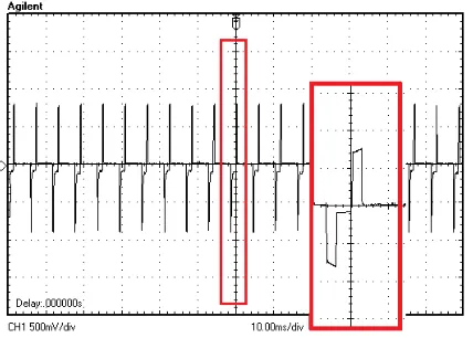
In-vitro test has been used for the proposed stimulator. A typical DBS electrode (Model 3988) was put into the Saline Solution (NaCl 0.9%) which represents the tissue solution. The experimental test has been done with various stimulation parameters. For example, Figure 6 shows the measured voltage across the electrode where the current is programmed to be 1.5 mA with the pulse duration of 100 µsec. In order to check the stimulator’s precision, different values of the output currents have been programmed and their actual current value was measured. The results are shown in Table. 1 and as it can be seen, the deviation of the current from its desirable value is less than 30 µA in any case, showing that the digital feedback loop works properly. Finally, the voltage across the Cdl was measured. The results show that it was was less than
24 mV for whole stimulation parameters. This remaining voltage is well below the critical value which is water oxidation potential voltage (e.g. ±50 mV).
Volume 3, Issue 4, April 2014
Page 309
Table 1: Deviation between the desired and actual current values.
Desired Stimulation
Current (mA)
Actual value
(mA) Deviation (µA)
1.2 1.18 20
1.8 1.79 10
2.6 2.59 10
3.1 3.08 20
4.5 4.42 30
6 5.99 10
4. Conclusion
This work presented a low power current stimulator which used a digital calibration technique to increase the accuracy of the output current. The quiescent of this stimulator has been reduced by using the low power and low sampling rate SAR ADC acting instead of power consuming OPAMP. Besides, a low area and low power charge balancing method has been introduced which uses no extra switch and pulse generator for electrode shortening phase. The remaining voltage across electrode is minimized due to precise current setting and the following charge balancing. This helps prevent damage and corruption in both electrode and tissue.
References
[1] V. Valente, A. Demosthenous, and R. Bayford, “A Tripolar Current-Steering Stimulator Asic for Field Shaping in Deep Brain Stimulation,” Biomedical Circuits and Systems, IEEE Transactions on, vol. 6, no. 3, pp. 197–207, 2012.
[2] H.-M. Lee, H. Park, and M. Ghovanloo, “A Power-Efficient Wireless System With Adaptive Supply Control for Deep
Brain Stimulation,” Solid-State Circuits, IEEE Journal of, vol. 48, no. 9, pp. 2203–2216, 2013.
[3] R. J. Coffey, “Deep Brain Stimulation Devices: A Brief Technical History and Review,” Artificial organs, vol. 33, no.
3, pp. 208–220,2009.
[4] S. Santaniello, G. Fiengo, L. Glielmo, and W. M. Grill, “Closed-loop control of deep brain stimulation: a simulation study,” Neural Systems and Rehabilitation Engineering, IEEE Transactions on, vol. 19, no. 1, pp. 15–24, 2011.
[5] K. Arfin, R.Sarpeshkar ,“An Energy-Efficient, Adiabatic Electrode Stimulator With Inductive Energy Recycling and
Feedback Current Regulation,” Biomedical Circuits and Systems, IEEE Transactions on vol. 6, no. 1, 2012.
[6] M. Ortmanns, A. Rocke, M. Gehrke, and H.-J. Tiedtke, “A 232-Channel Epiretinal Stimulator Asic,” Solid-State Circuits, IEEE Journal of, vol. 42, no. 12, pp. 2946–2959, 2007.
[7] K. Sooksood, T. Stieglitz, and M. Ortmanns, “An Active Approach for Charge Balancing in Functional Electrical Stimulation,” Biomedical Circuits and Systems, IEEE Transactions on, vol. 4, no. 3, pp. 162–170, 2010.
[8] W. Liu, K. Vichienchom, M. Clements, S. C. DeMarco, C. Hughes, E.McGucken, M. S. Humayun, E. D. Juan, J. D. Weiland, and R. Greenberg, “A Neuro-Stimulus Chip With Telemetry Unit for Retinal Prosthetic Device,” IEEE J. Solid-State Circuits, vol. 35, no. 10, pp. 1487–1497, Oct. 2000.
[9] S. C. DeMarco, L.Wentai, P. R. Singh, G. Lazzi, M. S. Humayun, and J. D.Weiland, “An Arbitrary Waveform Stimulus Circuit for Visual Prostheses Using a Low-Area Multibias DAC,” IEEE J. Solid-State Circuits, vol. 38, no. 10, pp. 1679–1690, Oct. 2003.
[10]M. Sivaprakasam, W. Liu, M. Humayun, and J. D. Weiland, “A Variable Range Biphasic Current Stimulus Driver Circuitry for an Implantable Retinal Prosthetic Devices,” IEEE J. Solid-State Circuits, vol. 40, no. 3, pp. 763–771, Mar. 2005.
[11]M. Bak, J. P. Girvin, F. T. Hambrecht, C. V. Kufta, G. E. Loeb, and E.M. Schmidt, “Visual Sensations Produced by Microstimulation of The Human Occipital Cortex,” Med. Biol. Eng. Comput., vol. 28, pp. 257–259, May 1990.
[12]M. Ghovanloo and K. Najafi, “A Compact Large Voltage Compliance High Output-Impedance Programmable Current Source for Implantable Microstimulators,” Biomedical Engineering, IEEE Transactions on, vol. 52, no. 1, pp. 97–105, 2005.
[13]X. Liu, A. Demosthenous, and N. Donaldson, “A fully integrated fail-safe stimulator output stage dedicated to fes stimulation,” in Circuits and Systems, 2007. ISCAS 2007. IEEE International Symposium on. IEEE, 2007, pp. 2076–2079.
Volume 3, Issue 4, April 2014
Page 310
[15]R. Shulyzki, K. Abdelhalim, A. Bagheri, C.M. Florez, P.L. Carlen, R. Genov “256-Site Active Neural Probe and 64-Channel Responsive Cortical Stimulator,” Custom Integrated Circuits Conference (CICC), 2011 IEEE, On page(s): 1 – 4.
[16]D. R. Merrill, M. Bikson, and J. G. Jefferys, “Electrical Stimulation of Excitable Tissue: Design of Efficacious and Safe Protocols,” Journal of neuroscience methods, vol. 141, no. 2, pp. 171–198, 2005.
AUTHOR
Farhad Bozorgi received the B.S. degree in electrical engineering from the Khaje Nasir Toosi University of Technology, Tehran, Iran, in 2011, and the M.Sc. degree in electronic engineering Circuits and Systems from the University of Tehran, Tehran, Iran in 2014. His current research is in Analog Circuit Designs, Microelectronics and Bioelectronics especially in Deep Brain Stimulation (DBS).
Reza Ranjandish Received the B.S. degree in electrical engineering from Shahid Beheshti University, Tehran, Iran, in 2011 and the M.Sc. degree in electrical engineering, in the Circuits and Systems Group from University of Tehran, Tehran, Iran, in
2014. His current research includes designing low power stimulators, impedance spectroscopy, charge balancing methods and neural recording as well as communication systems for Implantable Medical Devices (IMD).
Sina Ghanbari Received his B.S. degree in electrical engineering from Shahid Beheshti University, Tehran, Iran, in 2011 and his M.Sc. degree in electrical engineering, in the Circuits and Systems Group from University of Tehran, Tehran, Iran, in
2014. His current research includes digital systems’ reliability control, lower power and reliable digital circuit design, AVF analysis for multicore and many-core structures as well as digital systems for Implantable Medical Devices (IMD).