Volume 9, Number 3, pp. 185–196.http://www.scpe.org c 2008 SCPE
EFFICIENT IMPLEMENTATION OF WIMAX PHYSICAL LAYER ON MULTI-CORE ARCHITECTURES WITH DYNAMICALLY RECONFIGURABLE PROCESSORS
WEI HAN, YING YI, MARK MUIR, IOANNIS NOUSIAS, TUGHRUL ARSLAN, AHMET T. ERDOGAN
Abstract. Wireless internet access technologies have significant market potential, especially the WiMAX protocol which can offer data rate of tens of Mbps. A significant demand for embedded high performance WiMAX solutions is forcing designers to seek single-chip multiprocessor or multi-core systems that offer competitive advantages in terms of all performance metrics, such as speed, power and area. Through the provision of a degree of flexibility similar to that of a DSP and performance and power consumption advantages approaching that of an ASIC, emerging dynamically reconfigurable processors are proving to be strong candidates for future high performance multi-core processor systems. This paper presents several new single-chip multi-core architectures, based on newly emerging dynamically reconfigurable processor cores, for the WiMAX physical layer. A simulation platform is proposed in order to explore and implement various multi-core solutions combining different memory architectures and task partitioning schemes. The paper describes the architectures, the simulation environment, several task partitioning methods and demonstrates that up to 4.9x speedup can be achieved by employing five dynamically reconfigurable processor cores each having individual local memory units.
Key words: multi-core, WiMAX, dynamically reconfigurable, SystemC
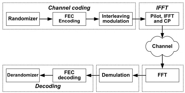
1. Introduction. Since the advent of the internet, people have come to depend on it more and more. There is an increasing desire to access it at any time from anywhere. Obviously, cable based internet cannot satisfy this demand. The wireless internet protocol was born in 1997 when IEEE 802.11 [1] was released. In the last decade, more standards have emerged with higher and higher data rates as well as longer and longer ranges. The IEEE 802.16 standard is a wireless broadband access standard which helps make the vision of pervasive connectivity a reality [2]. WiMAX (Worldwide Interoperability for Microwave Access) is its commercial name. WiMAX technology can provide up to tens of Mbps symmetric bandwidth over many kilometers. This gives WiMAX a significant advantage over other alternatives like Wi-Fi and DSL. The physical layer of WiMAX includes both downlink (channel coding and IFFT) and uplink (FFT, modulation and decoding) data processing, as shown in Fig. 1.1. WiMAX applications demand high performance, strict low power, and in-field reprogrammability to follow the evolving standard. Recently, some solutions have been proposed for industry targeting WiMAX that are based on multi-core processor systems, such as [3, 4]. Ever since the first effort to design a parallel machine (called SOLOMON) failed in 1958 [5], the parallel computing paradigm has been improved dramatically. Within the past half century, many advanced technologies have been created and became popular, such as single instruction multiple data (SIMD), symmetric multiprocessing (SMP) and multithreading. The rapid development and demand for parallel architectures are driven by application trends, semiconductor technology trends, and microprocessor and system design trends [6]. Again compelled by those trends, parallel architectures are applied to smaller and smaller computer systems, from the original mainframes, to servers, and to PCs, and now even to embedded systems. Twenty years ago, an 8-bit microcontroller could satisfy most of the requirements of embedded systems. But now, even an advanced 32-bit reduced instruction set computer (RISC) processor may not be able to realize a complicated embedded application. Moreover, as more and more complex applications are mapped onto embedded systems, and the concern about power consumption and heat dissipation increases, there is a need to distribute the processing load of large embedded programs over multiple processors. A multi-core processor gains the advantage over multi-chip SMP in terms of all performance metrics, due to the shorter distances the signals between processors have to travel. Here a multi-core processor (or multi-core) is defined as a single chip combining two or more independent general purpose processor or DSP cores.
Today’s common general-purpose processors or DSPs cannot satisfy all the features required by current and future embedded systems, including higher performance, higher power efficiency and higher flexibility. Filling the gap between the high flexibility of DSPs and the high performance of ASICs, dynamically reconfigurable (DR) processors offer an alternative solution for embedded systems. This paper extends our work in [27] and presents several new single-chip multi-core architectures, based on newly emerging dynamically reconfigurable processor cores, for the WiMAX physical layer. To address this, we have proposed a flexible simulation platform that enables the analysis and investigation of multi-processor systems based on coarse-grained DR processors— an area that as yet has been little explored. The WiMAX 802.16-2004 physical layer was ported on this platform.
Randomizer EncodingFEC Interleaving modulation
Pilot, IFFT and CP
Channel
FFT Demulation
FEC decoding Derandomizer
Channel coding
Decoding
IFFT
Fig. 1.1.WiMAX physical layer processing chain
The rest of this paper is organized as follows: section 2 reviews related research work on both WiMAX implementations and multi-core processor solutions for embedded systems. Section 3 provides a brief overview of the target dynamically reconfigurable processor and introduces the underlying multi-core processor architecture within the platform. Section 4 presents a SystemC TLM based simulator which models this multi-core processor architecture. Section 5 describes how to map multiple tasks onto the multi-core processor architecture and several different task partitioning scenarios for efficiently implementing WiMAX physical layer on the multi-core processor simulator, the results of which are shown in section 6. Finally, conclusions are given in section 7.
2. Related Work.
2.1. WiMAX Implementations. Many market-leading companies today provide products based on silicon implementations of WiMAX standards. Such products include ASIC, DSP or network processor tech-nologies. For example, Wavesat DM256 [11] is an ASIC solution, and the Intel NetStructure WiMAX Baseband Card is based on the Intel IXP2350 network processor [12], while both Freescale MSC8126 DSP [3] and Picochip PC203 [4] use the multi-core DSP approach. In [13], a multitasked version of the WiMAX physical layer has been mapped onto a single DR architecture with a real-time operating system (RTOS) -µC/OS - II.
2.2. Chip-level Multiprocessor in the Embedded Field. System architects today acknowledge that higher clock rates, deeper pipelining, and increasing instruction-level parallelism (ILP) cannot be relied on any more in order to increase performance. This is due to overheads introduced by such techniques. For this reason, industry has started looking at multi-core processor solutions. Besides multi-core DSPs mentioned above, other multi-core processor products include Cell Broadband Engine Architecture [18], ARM11 MPCore [20], intellaSys SEAforth-24A [21], and Ambric Am2000 family [19]. Few multi-core processor projects are based on coarse-grained DR processors: One such example being the work on developing a multi-core processor based on the Montium Tile Processor (TP) from RECORE [14]. However, to the best of our knowledge, currently Montium TP does not support development from high-level languages, and its homogeneous processing part array (PPA) is not efficient in terms of hardware resource occupancy. While our chosen DR processor can provide high performance at low power and area, addressing all the desired requirements for future portable devices. The cell array configuration can be tailored towards different application domains. A series of power saving techniques have been adopted, which include using registers for interim storage, avoiding large multiplexers and multiple-load busses, increasing the program kernel, and using heterogeneous instruction cells.
3. Multiple Reconfigurable Processor Architecture.
that it is largely indistinguishable from a conventional processor, except for the memory access patterns (for both data and program memory) which can be quite different. This is one of the key issues addressed in this research. It supports operation chaining—the ability to execute both dependent and independent instructions in parallel, which leads to high degree of parallelism. This demands higher data memory bandwidth in order to keep the array fed with data, a demand which has been met by providing a multi-bank memory system that is quite different to that seen in conventional processor based multi-core processor systems. Furthermore, the instruction stream fetch patterns are unusual in that successive iterations of certain loops can be executed following only a single fetch. The instruction words are also quite large compared to those in existing DSPs. ANSI-C programs can be compiled into a sequence of configuration contexts, the contents of which are executed concurrently by the DR processor according to the availability of hardware resources. Formed by a sophisticated scheduling algorithm [10], each context packs together as many chains of operations as possible, and takes a variable number of clock cycles to execute, in order for all chains to complete. Another salient characteristic of the DR processor is that it is tailorable and extensible, and can be customised at design stage according to the application requirements. A number of algorithms have been tested to demonstrate that the target processor can achieve up to 6 times less energy consumption than a DSP such as a TI very long instruction word (VLIW) and 8 times higher throughput than RISC CPUs such as OR32 [9].
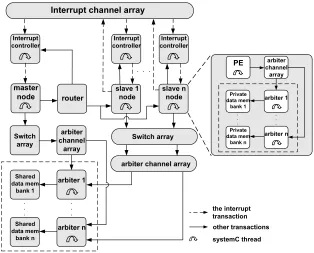
3.2. Master-Slave Shared Memory Architecture. In this paper, we propose a master-slave based shared memory architecture for DR processors (shown in Fig. 3.1), targeting WiMAX applications. The shared memory architecture is popular for multiprocessors based on a small number of cores. One of the key aspects of this architecture is that it provides support for DR processors that may issue multiple concurrent memory access requests per cycle. This architecture consists of one master processor core and multiple slave processor cores. The main difference between the master and slaves is that the master core takes charge of the task management. When the system starts up, the master dispatches tasks to slaves by sending the task information through a router. When a slave finishes its current job, it sends an interrupt to the master, requesting a new job. Then the master runs a corresponding interrupt handler to dispatch a new job to that slave. The target DR processor is used for both master and slave cores, since it is suitable for executing both data path and control path programs, as presented in [13], where both a RTOS and WiMAX protocol run concurrently on a single DR architecture. To address the parallel memory access requirement of DR processors, this multi-core processor architecture is based on a Harvard architecture where each core owns a program memory and all processor cores share a multi-bank based data memory. Besides the shared data memory, each DR processor core can have its own local private multi-bank data memory which cannot be addressed by other processors. By having much smaller access latency than the shared memory, due to the adjacency to the processor and smaller depth, the private memory alleviates the conflict in accessing the shared memory, and improves the data locality, and therefore improves the throughput. Each data memory bank has an arbiter which arbitrates the memory accesses to the bank from different processor cores or different memory ports of the same DR processor core, which may contain multiple memory access ports. All shared data memory banks are connected to all processor cores through switch bars. According to the number of banks and the referenced address, each memory access request to the shared data memory from a memory port of a processor core is routed through switches to the proper arbiters. Each processor core has one local interrupt controller. An interrupt channel array is provided for communication transactions between interrupt resources and interrupt controllers.
Interrupt controller master node router . . . Interrupt controller slave 1 node Interrupt controller slave n node
Interrupt channel array
arbiter 1 Shared data mem bank 1 arbiter channel array Switch array arbiter n Shared data mem bank n . . . . . .
arbiter channel array Switch array systemC thread the interrupt transaction other transactions PE arbiter 1 Private data mem bank 1 arbiter channel array arbiter n Private data mem bank n . . . . . .
Fig. 3.1.Master-slave shared data memory architecture
file into independent banks with a reduced number of ports per bank for reducing the number of register file ports. MEM Access MEM Access MEM Access RI0
ADD SHIFT MUL
COMP
MUL LOGIC RI2
RI3
LOGIC ADD MUL RI1
Arbiter 0 MEM Access MEM Access MEM Access RI3
ADD SHIFT MUL
COMP
MUL LOGIC RI1
RI0
LOGIC ADD MUL RI2
Register File Bank 0
Arbiter 1
Register File Bank 1
Arbiter 2
Register File Bank 2
Arbiter 3
Register File Bank 3
. . .
Fig. 3.2.The shared register file implementation
fixed register file bank. For example, register file interface cell RI0 is only connected to bank0 and register file interface cell RI1 can only access bank1. This scheme keeps all possible connections between the instruction cell and the shared register bank with a reduced MPSoC interconnection complexity.
The existing DR processor tool-flow provides full support for the inclusion of both combinatorial and synchronous custom instruction cells through the simulator libraries. The function descriptions of the custom cells such as the interface cells are modeled in C++ via template classes provided by the simulator. A fully automated system generator compiles the standard simulator libraries with the custom cell objects and generates all the required support files and the custom simulator, replacing the standard simulator used in the DR processor tool flow. The shared register file has been synthesised with Cadence Ambit BuildGates using the UMC 0.18um standard CMOS cell library which the DR processor is based on. The power consumption of the synthesized register file has been obtained using Synopsys PrimePower. The generated timing, area and power information is used in the DR processor tool flow for scheduling and simulation purposes.
3.4. Atomic Operation Support. In order to avoid race conditions caused by simultaneous accesses to a shared resource from different processes, in this work the process synchronization was implemented with the use of spinlocks. A spinlock is a lock where a task repeatedly checks the lock (synchronization variable)—a method called busy-waiting. A spinlock allows only one task to access the shared resource protected by the lock at any given time. Implementing a spinlock requires the support of atomic read-modify-write operations where the content of a memory location is guaranteed to be read, modified and written back without intervening operations from other processor cores. In this work, a pair of special instructions—load-linked and store-conditional (i. e. LL/SC) [6] are used to implement atomic operations and therefore the spinlock. The idea behind the LL/SC is that LL loads the synchronization variable into a register, and is immediately followed by an instruction that manipulates the variable. For the spinlock, this instruction adds 1, then SC tries to write the variable back to the memory location if and only if the location has not been written by other processor cores after LL was completed by this processor core [6]. A pseudo-assembly code for the spinlock and unlock algorithms implemented by LL/SC is shown below [6]:
Lock: LL reg1, location // LL the variable BNZ reg1, lock // if locked, try again SC location, reg2 //SC the variable BEQZ lock //failed, try LL again
Unlock: WRITE location, 0 //write 0 to location
In the proposed multiprocessor architecture, for implementing LL/SC, each data memory arbiter contains a hardware lock flag and a lock address register for each processor. When an LL instruction from one processor reads a synchronization variable, the corresponding lock flag is set and the variable address is stored into the corresponding lock address register. Whenever the referenced address of a write request (either normal write or SC) is matched against the value of the lock address register, the lock flag is reset. A SC instruction enables a check of the lock flag. If it has been reset, meaning that an intervening conflicting write occurred before, SC fails, otherwise, it succeeds.
Obviously, the busy-waiting based spinlock causes more memory access conflicts and more power consump-tion since the waiting core keeps checking the synchronizaconsump-tion variable. In this paper, we have presented an optimized method, called Lock&Signal, which can reduce the memory access competition and therefore the power consumption. The idea is that if the lock required by a processor core is unavailable, the task will go to sleep and the processor core will do nothing but wait. When the lock is released by another process, the releasing process will send a signal to the waiting process, informing it that the lock is now available, through an inter-processor interrupt. Then the waiting process can resume its operation. Therefore, memory access conflicts due to the busy-waiting based spinlock, which may take up a reasonable ratio of the execution time, are eliminated.
system simulator, by feeding timing information to it. Obviously, the simulation speed is dramatically decreased since Simics is involved during the multiprocessor simulation. While SESC simulator [32] uses the instruction streams generated by MINT, an emulator for MIPS architecture, to model chip-level multiprocessors with out-of-order processors. In [33], a simulation environment called MPARM is proposed based on SystemC register transfer level (RTL) and SWARM (software ARM) simulator. However, partially describing the system at lower SystemC abstraction level, MPARM is inevitably slower than a TLM based simulation tool. Moreover, most of these simulation tools are designed for multiprocessors with conventional processor architectures like ARM and MIPS. To the best of our knowledge, there has been little research done for developing TLM based simulation tools for MPSoCs targeting coarse-grained DR processors (e.g., [9]).
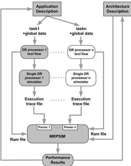
TLM is a higher abstraction level than RTL, and is a transaction-based modeling approach which enables concurrent hardware/software co-design for early software development, architecture analysis and functional verification. In TLM, system components are modeled as modules containing a number of concurrent SystemC threads which represent their behavior. The communication among modules is achieved using transactions through abstract channels which implement TLM interfaces. As the kernel of TLM, TLM interfaces can be accessed by SystemC threads through module ports [16]. Fig. 3.1 illustrates how the architecture is imple-mented using TLM. The master processor core, slave processor cores and arbiters are modeled as initiators which contain SystemC threads initiating transactions to the target components such as memory banks and the router. Meanwhile, an initiator could be a target as well, like the processor cores which also can receive interrupt transactions from the interrupt controllers. Based on run-time communication between the memory system and the DR processors, our multi-core processor simulator maintains the timing accuracy with a rapid architecture analysis. The generated TLM executable, which is called multiple reconfigurable processor sim-ulator (MRPSIM), is parameterizable in terms of the number of slave processor cores, the number of shared memory banks, inter-process communication methods, single core or multi-core model and so on. For example, by setting an option, each DR processor core can have its own local private memory which stores the local data for the associated tasks on the processor core, while the shared data memory is only used for global data and synchronization variables.
MPSIM is a trace-driven simulator. The advantage of the trace-driven simulation over execution-driven simulation is that once the trace has been collected, it can be reused as a constant input to the simulator when the MPSoC architecture varies. However, a difference from other trace-driven simulators - which sacrifice accuracy for performance - MRPSIM can maintain the timing accuracy with a rapid architecture analysis. The idea is that the functionality of the programs and the calculation of static timing are decoupled from dynamic timing simulation. In our simulation approach, the entire simulation timing is separated into static timing and dynamic timing. Static timing represents the time consumed by the combinatorial critical path in each configuration context. It is not affected by the run-time execution. Dynamic timing refers to the time taken by communication instructions (e.g., load and store memory), which can only be determined during at run-time in the multiprocessor simulation, due to competition such as from multiple processors, or multiple memory accesses from one of the processors.
To implement this approach, each program to be executed on MRPSIM should first be executed on a single DR processor simulation model. MRPSIM uses static timing and instruction information from the execution traces provided by the single DR processor simulator to determine the length of time each processor core is occupied between memory accesses. Then, the dynamic delays imposed by memory access, process synchronization and interrupts are obtained from the run-time behaviour of the TLM model. Through this method, MRPSIM can correctly and efficiently simulate the run-time multi-core processor environment, allowing the throughput of the modeled system to be measured. This approach is well suited to programs with simple control flow, such as the WiMAX physical layer.
5. Mapping Methodology and Task Partition.
DR processor 1 tool flow
task1 +global data
. . . .
Ram file
taskn +global data Application
Description
Architecture Description
Single DR processor n
simulator Single DR
processor 1 simulator
Execution trace file
Execution trace file
Performance Results . . . .
. . . .
Parser 1 Parser n
MRPSIM . . .
Ram file DR processor n
tool flow
Fig. 5.1.Mapping methodology
timing information for configuration contexts. After that, parsers within MRPSIM convert those machine-specific execution trace files into a machine-independent intermediate representation that captures the timing model and flattened program control flow structure. Through this method, the multi-core processor model can support both homogeneous and heterogeneous DR processor based multi-core architectures, or even conventional DSPs. Other inputs of MRPSIM include the RAM files describing the layout of data symbols in the various data memories, and an architecture description file which contains information for both the multi-core processor architecture and the single DR processor. After performing simulations with MRPSIM, generated results are used as feedback to change the design strategy such as the task partitioning and architecture parameters in order to achieve better performance.
5.2. Task Partition Methods. Important issues in multi-processor System-on-Chip (MPSoC) designs are the communication infrastructure and task mapping. We use profiling-driven partition and static mapping solutions. The execution time of a task performed by a single processor can be obtained by software profiling using an instruction set simulator. Task merging and task replication are two main process transformations to improve the application throughput [17]. The WiMAX physical layer application consists of five tasks defined in [13], which are channel coding, IFFT, FFT, demodulation and decoding, as shown in Fig. 1.1, with individual execution times of 60us, 108us, 109us, 28us and 1206us, respectively. The design challenge is to map the application onto an architecture optimized in terms of the system performance and cost. This includes not only the mapping strategy but also architectural design choices such as the number of processor cores and each processor’s make up in terms of number of instruction cells and their types.
Channel coding Time = 60us
IFFT Time = 108us
FFT Time=109us
Demodulation
Time = 28us Time=1206us Decoding
Processor 1 channel coding, IFFT, FFT, Demodulation Time = 305us
Processor 2
Decoding Time = 1206us (merge)
Processor 3
Decoding Time = 1206us
Processor 4
(Replication)
Decoding Time = 1206us
Processor 5
Decoding Time = 1206us
(a) Task Merging (a) Task Replication
Fig. 5.2.Task Merging and Task Replication Methods
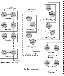
Processor 2 Butterfly_15 Processor 1 Butterfly_8-11 Butterfly_0-3 Butterfly_4-7 Butterfly_12-15 Butterfly_15 Butterfly_2 Butterfly_1 Indep. Datapath Dep. Datapath Butterfly_0 Indep. Datapath Dep. Datapath Indep. Datapath Dep. Datapath
(a) A single processor
(b) Two processors Indep. Datapath Dep. Datapath Indep. Datapath Dep. Datapath Indep. Datapath Dep. Datapath
Loop 870 times
Indep. Datapath Dep. Datapath Indep. Datapath Dep. Datapath
Loop the first 670 times Butterfly_0 Indep. Datapath Dep. Datapath Indep. Datapath Dep. Datapath
Loop the last 200 times
Fig. 5.3.Loop Partitioning Method
body of the main loop of the decoding task iterates 870 times and includes 16 butterfly operations. A butterfly operation consists of independent and dependent data paths. The independent data paths can be run on different processor cores to increase the instruction level parallelism. Loop splitting is a compiler optimization technique that attempts to simplify a loop or eliminate dependencies by breaking it into multiple loops which have the same bodies but iterate over different contiguous portions of the index range. To make use of this idle time, loop splitting can be used to effectively move some of the work of the decoding task from the second processor onto the first processor, during this idle time. To achieve this, the decoding loop body is written in two ways: one with all the work being done on a single processor, and another where some of the butterflies are moved to another processor, such that they can be performed in parallel, but out of sync to allow for the dependencies to be met. The second processor then runs the first (single-processor) version when the first processor is busy executing the merged tasks, then switches to the second version (dual-processor), allowing the now idle first processor to share in the decoding task. Based on the execution time of the merged task, the loop is split into two parts: the first 670 iterations and the last 200 iterations. The execution time of the last 200 iterations is nearly equal to the merged task. The body of the loop in the first 670 iterations is partitioned across two processor cores, as shown in Fig. 5.3(b). After loop partitioning, the merged task and part of the first 670 iterations are assigned to one processor core, the remaining part of the first 670 iterations and the whole of the last 200 iterations are assigned to the second processor core. The first processor’s idle time can be best absorbed in this way by executing the dual-processor version of the decoding task for 670 iterations. The loop partitioning results in a balanced workload; however it may introduce a large number of data exchange between cooperating processor cores and increase communication overhead. If the data exchange happens in the shared memory, the shared memory could become a performance bottleneck of the loop partitioning method due to the frequent additional data communication between the DR processors. Therefore, a feasible optimization method is mapping the frequent read and write shared data to the shared register file for reducing memory access time and memory access conflicts.
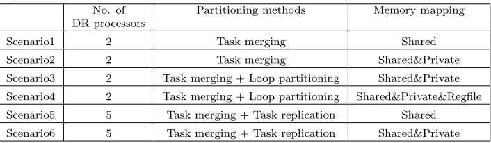
6. Results. Several WiMAX multiprocessing scenarios, which combine different task partitioning methods and memory architectures, have been implemented and simulated with MRPSIM. These scenarios are described in Table 6.1. To make fair performance comparisons, all scenarios are executed with 100 OFDM symbols. The clock frequency of the DR processor was set to 500MHz and the shared memory access delay was set to 6ns, the local private memory access delay was set to 2ns, and the shared multi-bank register file access delay is 1ns. Meanwhile, the WiMAX was executed on the single processor simulator with the same simulation parameters except the local private memory and shared register file, for comparison.
Table 6.1 Multiprocessing scenarios
No. of Partitioning methods Memory mapping
DR processors
Scenario1 2 Task merging Shared
Scenario2 2 Task merging Shared&Private
Scenario3 2 Task merging + Loop partitioning Shared&Private
Scenario4 2 Task merging + Loop partitioning Shared&Private&Regfile
Scenario5 5 Task merging + Task replication Shared
Scenario6 5 Task merging + Task replication Shared&Private
1.154 1.28
3.99
4.92
1.47 1.55
0 1 2 3 4 5 6
Scenario 1 Scenario 2 Scenario 3 Scenario 4 Scenario 5 Scenario 6
S
p
e
e
d
u
p
Fig. 6.1.The speedup of scenarios over a single DR processor
0.577 0.64
0.772 0.798
0.984
0.734
0 0.2 0.4 0.6 0.8 1 1.2
Scenario 1 Scenario 2 Scenario 3 Scenario 4 Scenario 5 Scenario 6
P
a
ra
lle
l
e
ff
ic
ie
n
c
y
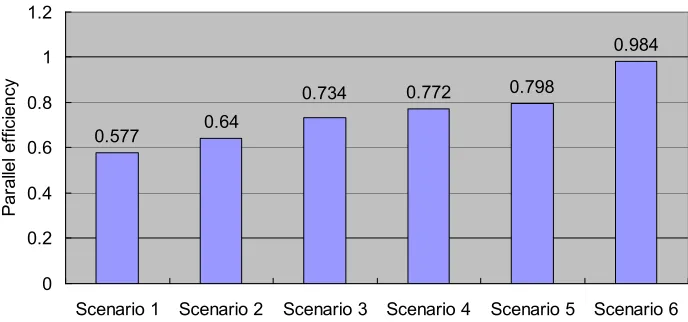
Fig. 6.2.The parallel efficiency of scenarios
memory have better throughput compared to their counterparts which have shared data memory only. Sce-nario 6 with local memory achieved 4.92x speedup and a parallel efficiency of 0.98 with five target DR processor cores. Due to the deeply imbalanced workload, scenarios only using task merging demonstrate very high idle ratios for the processor cores. Based on the multi-core architecture with limited processor cores, scenario 4, which uses task merging and loop level partitioning, has a much lower total idle ratio and better performance compared to scenarios using task merging only. This is due to the improved instruction level parallelism and the efficient multi-core architecture with a shared register file between different processor cores.
Table 6.2
The idle ratio of each PE for individual scenarios
PE0 PE1 PE2 PE3 PE4 Average
(master) (Slave0) (Slave 1) (Slave 2) (Slave 3)
Scenario1 73.5% 0.3% - - - 36.9%
Scenario2 75.9% 0.2% - - - 38.1%
Scenario3 12.2% 10.5% - - - 11.4%
Scenario4 14.3% 9.6% - - - 12.0%
Scenario5 3.5% 8.4% 8.3% 8.3% 8.4% 7.2%
Scenario6 7.4% 7.4% 3.7% 3.7% 3.7% 5.2%
methods have been applied, and their impact on the system performance has been discussed. A flexible multi-core processor simulation platform, MRPSIM, has been proposed and developed in order to evaluate different solutions which combine different task partitioning strategies and memory architectures. Simulation results have demonstrated the effectiveness of the proposed strategies in terms of speedup and parallel efficiency.
REFERENCES
[1] IEEE 802.11-1997: Wireless LAN Medium Access Control (MAC) and Physical Layer (PHY) Specifications, 1997. [2] IEEE Standard for Local and Metropolitan Area Networks, IEEE STD 802.16-2004, 2004.
[3] Implementing WiMAX PHY Processing Using the Freescale MSC8126 Multi-Core DSP, Freescale Semiconductor WiMAX WP White Paper, April 2004.
[4] Picochip PC203 produce brief, Picochip.
[5] G. Wilson,The History of the Development of Parallel Computing,http://ei.cs.vt.edu/ history/Parallel.html
[6] David Culler, J.P. Singh and A. Gupta,Parallel Computer Architecture: A Hardware/Software Approach, Morgan Kauf-mann, 2nd edition 1999.
[7] HiveFlex programmable cores, www.siliconhive.com
[8] Carl Ebeling, Chris Fisher, Guanbin Xing, Manyuan Shen, Hui Lui,Implementing an OFDM Receiver on the RaPiD Reconfigurable Architecture, IEEE Trans. Computers, Vol. 53, No. 11, Nov. 2004, pp. 1436–1448.
[9] S. Khawam, I. Nousias, M. Milward, Y. Yi, M. Muir and T. Arslan,The Reconfigurable Instruction Cell Array, IEEE Transactions on Very Large Scale Integration (VLSI) Systems, Vol. 16, Issue 1, pp. 75–85, Jan. 2008.
[10] Y. Yi, I. Nousias, M. Milward, S. Khawam, T. Arslan and I. Lindsay,System-level Scheduling on Instruction Cell Based Reconfigurable Systems, Design, Automation and Test in Europe (DATE 06), Vol. 1, pp. 1–6, March 2006.
[11] WiMAX 3.3-3.8GHz Mini-PCI Reference Design Series, Wavesat, 2007.
[12] Intel NetStructure WiMAX Baseband Card Product Brief, Intel Corporation, 2006.
[13] W. Han, I. Nousias, M. Muir, T. Arslan and A. T. Erdogan,The Design of Multitasking Based Applications on Recon-figurable Instruction Cell Based Architectures, Int. Conf. on Field Programmable Logic and Applications (FPL 2007), pp. 447–452, Aug. 2007.
[14] P. Heysters and G. Smit,Mapping of DSP algorithms on the MONTIUM architecture, Parallel and Distributed Processing Symposium, April 2003.
[15] A system description language,http://www.systemc.org
[16] A. Rose, S. Swan, J. Pierce and J. M. Fernandez,Transaction level modeling in SystemC, Open SystemC Initiative 2005. [17] C. Ostler and K.S. Chatha,An ILP Formulation for System-Level Application Mapping on Network Processor
Architec-tures, Design, Automation & Test in Europe (DATE ’07), pp. 1–6, April 2007.
[18] D. Pham, S. Asano, M. Bolliger, M. N. Day, H. P. Hofstee, C. Johns, J. Kahle, A. Kameyama, J. Keaty, Y. Masub-uchi, M. Riley, D. Shippy, D. Stasiak, M. Suzuoki, M. Wang, J. Warnock, S. Weitzel, D. Wendel, T. Yamazaki, and K. Yazawa,The design and implementation of a first-generation CELL processor, IEEE International Solid-State Circuits Conference (ISSCC 2005), pp. 184–592, Vol.1, 2005.
[19] M. Butts, A. M. Jones, and P. Wasson, A Structural Object Programming Model, Architecture, Chip and Tools for Reconfigurable Computing, 15th Annual IEEE Symposium on Field-Programmable Custom Computing Machines (FCCM 2007), pp. 55–64, 2007.
[20] Kazuyuki Hirata and John Goodacre,ARM MPCore The streamlined and scalable ARM11 processor core, Asia and South Pacific Design Automation Conference (ASP-DAC ’07), pp. 747–748, 2007.
[21] Seaforth-24 Device Data Sheet, intellaSys,http://www.intellasys.net
[22] V. Zyuban and P. Kogge,The energy complexity of register files, the 1998 international symposium on Low power electronics and design, pp. 305–310, 1998.
[23] V. V. Zyuban and P. M. Kogge,Inherently lower-power highperformance superscalar architectures, IEEE Transactions on Computers, 50(3): 268–285, March 2001.
[24] Jos, C. Lorenzo, G. Antonio, lez, V. Mateo, and P. T. Nigel,Multiple-banked register file architectures, the 27th annual international symposium on Computer architecture, pp. 316–325, 2000.
[25] I. Park, M. D. Powell, and T. N. Vijaykumar,Reducing register ports for higher speed and lower energy, 35th Annual IEEE/ACM International Symposium on Microarchitecture (MICRO-35), pp. 171–182, 2002.
[26] Andr´e Seznec, Eric Toullec and Olivier Rochecouste, Register Write Specialization Register Read Specialization: A Path to Complexity-Effective Wide-Issue Superscalar Processors, 35th Annual IEEE/ACM International Symposium on Microarchitecture, (MICRO-35), pp. 383–394, 2002.
[27] W. Han, Y. Yi, M. Muir, I. Nousias, T. Arslan, and A. T. Erdogan,Efficient Implementation of Wireless Applications on Multi-core Platforms based on Dynamically Reconfigurable Processors, 2008 International Workshop on Multi-Core Computing Systems (MuCoCoS’08), 2008.
[28] M. Manjikian,Multiprocessor enhancements of the SimpleScalar tool set, Computer Architecture News (CAN), Vol. 29, Issue 1, pp. 8–5, March 2001.
[29] C. J. Hughes, V. S. Pai, P. Ranganathan and S. V. Adve,Rsim: simulating shared-memory multiprocessors with ILP processors, IEEE Trans. on Computer, vol. 35, Issue 2, pp. 40–49, Feb. 2002.
[30] M. M.K. Martin, et al.,Multifacet’s General Execution-driven Multiprocessor Simulator (GEMS) Toolset, Computer Ar-chitecture News, Vol.33, No.4, pp. 92-99 September 2005.
[31] J. D. Davis, C. Fu and J. Laudon,The RASE (Rapid, Accurate Simulation Environment) for chip multiprocessors, ACM SIGARCH Computer Architecture News, Vol. 33 Issue 4, pp. 14–23, November 2005.
[33] L. Benini, D. Bertozzi, A. Bogliolo, F. Menichelli, and M. Olivieri,MPARM: Exploring the Multi-Processor SoC Design Space with SystemC, Journal of VLSI Signal Processing, Vol. 41, pp. 169–182, Sept. 2005.
Edited by: Sabri Pllana, Siegfried Benkner Received: June 16, 2008