A New Solution to Analysis of CMOS Ring Oscillators
P. M. Farahabadi*, H. Miar-Naimi** and A. Ebrahimzadeh**
Abstract: New equations are proposed for frequency and amplitude of a ring oscillator. The method is general enough to be used for all types of delay stages. Using exact large-signal circuit analysis, closed form equations for estimating the frequency and amplitude of a high frequency ring oscillator are derived as an example. The method takes into account the effect of various parasitic capacitors to have better accuracy. Based on the loop gain of the ring, the transistors may only be in saturation or experience cutoff and triode regions. The analysis considers all of the above mentioned scenarios respectively and gives distinct equations. The validity of the resulted equations is verified through simulations using TSMC 0.18 µm CMOS process. Simulation results show the better accuracy of the proposed method compared with others.
Keywords: CMOS voltage-controlled oscillators, high-speed integrated circuits, trigonometric equations, large-signal analysis.
1 Introduction1
Voltage controlled oscillators (VCO) are most commonly used building blocks in communication applications like phase locked loops (PLL) and clock and data recovery circuits [1]-[5]. Due to lower power consumption, large tuning range and lower die space area, the ring oscillator (RO) is investigated in these applications. RO circuits must satisfy some specifications such as area, power, speed and phase noise, posing challenges to circuit and system designers. Also the correct amplitude and low phase noise are two criteria to obtain a suitable performance for VCO in a circuit. Obtaining the transfer function or any knowledge about the amplitude and frequency of the oscillator is necessary to overcome these tradeoffs [6]-[12]. Some simple mathematical equations have been presented for frequency of oscillation of the RO, commonly using small signal analysis [13]-[16]. All of these equations assume the RO as a linear small-signal circuit model and derive the oscillation frequency by adding the parasitic and secondary effects to the simple ideal frequency equation. However, because of the
Iranian Journal of Electrical & Electronic Engineering, 2009. Paper first received 20 Oct. 2008 and in revised form 16 Dec. 2008. * Payam M. Farahabadi is with the Integrated Systems Research Laboratory, Electrical and Computer Engineering Department, Babol University of Technology, Mazandaran, Babol.
E-mail: [email protected]
** The Authors are with the Babol University of Technology, Mazandaran, Babol.
E-mails: [email protected], [email protected].
inherent nonlinear behavior of the RO, the accuracy of the equations is limited only for these assumptions.
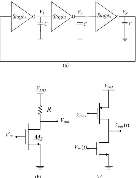
(a)
(b) (c)
Fig 1. (a) N-stage single-ended RO. (b) Delay stage, with
resistor load (c) Transistor Level load for delay stage.
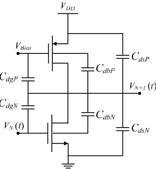
Fig. 2. Parasitic capacitors in a delay stage
Moreover, all of these equations cannot represent the amplitude of the output waveform of the RO exactly.
This paper presents a novel method to derive equations for both amplitude and oscillation frequency of the RO. In this method, the parameterized waveforms of the outputs are estimated and closed-form equations for unknown parameters are derived using differential equations. The rest of the paper is as follows: SECTION II introduces mathematical principle used to compute the frequency of oscillation and a brief review of the existing methods. Section III describes the proposed methodology to derive the equations for the amplitude and the frequency of oscillation. A new technique based on large signal analysis is presented to derive exact equations for the output frequency and amplitude in this section. Simulation results are compared with the values estimated by equations to show the validity of the method in section IV. Finally, section V gives the conclusions.
2 Literature Review on Frequency Equations A ring oscillator consists of a number of gain stages in a unity gain feedback loop. To achieve oscillation, the circuit must satisfy two Barkhausen’s criteria that mean the total phase shift and the gain of the feedback loop must be 2π and one respectively. An N-stage ring oscillator is shown in Fig. 1. Small signal analysis and the open loop transfer function for this circuit is written as below:
0
1 ( )
( ) [ ( || )] ( 1)
(1 )
N
N N m
m
N
g R
H s g R
s Cs
= − = −
+
ω
(1)
RC
/
1
0
=
ω
(2)Because of the unity feedback gain, the open loop transfer function is the same as the loop transfer function. Total phase shift around the loop is written as (3) and for ω = 0 it is written like equation (4) that means the oscillator locks at DC level for even N, so the odd number of stages is necessary for oscillation in single-ended ring oscillators [4].
1 0
( )= − −Ntan ( /− )
φ ω π ω ω (3)
0
2 2
( )
2 1
N n
N n
=
=
⎧
=⎨
= −
⎩
ω
π φ ω
π (4)
Total phase shift 2π for oscillation is provided at
ωosc for odd N by (5). Equation (5) is most commonly used for the oscillation frequency of an RO in analog microelectronic design text books [12].
0tan( / )
osc= N
ω ω π (5)
With simple simulations, one can find that this analysis is incorrect if the amplitude of outputs does not meet the small signal conditions. Also, small signal analysis does not give any idea about the amplitude of oscillation.
Considering RO as a chain of delay stages is another method which is also commonly used by designers. Assuming a delay of td for each stage, total phase shift 2π must be provided in the period of 2Ntd. Therefore, the oscillation frequency is as (6):
1 2 d
f
N t
=
⋅ (6)
A method to improve the accuracy of previous equation is proposed in [13]. The oscillation frequency in this method is given by (7). The set of parameters that have been used in this method is listed in Table 1.
The time delay per stage is defined as the total change in differential output of the midpoint of the transition. This method only considers differential RO and cannot be extended to single ended structures.
Reference [14] models each delay stage as a simple RC circuit. Using (8), with Vout(initial) equals to VDD
Table 1. Differential Delay Stage parameters
N Number of delay stages in the RO
td Delay time of each stage in the RO
RL
Equivalent resistance of the PMOS load of each delay stage
CL Load capacitance of the delay stage without
parasitic elements
ISS Tail current used in the differential delay stage
VSW Peak to peak amplitude of the output voltage
waveform
and Vout(final) equals to VDD-VSW, the delay per stage equals to RLCLln2. Hence the frequency is given by (9).
1 2 d
f
N t
=
⋅ (7)
( ) ( ) [ ( ) ( )]
exp( )
out out out out
V t V final V initial V final t
RC
= + −
× − (8)
1 2 L L ln 2 f
NR C
=
⋅ (9)
The method proposed in [15] assumes a ramp input to find delay to time constant to obtain (10).
1
2 (0.8) ( DBn DBp GDn GDp L) f
N R C C C C C
=
⋅ + + + + (10)
This equation can be adapted for single-ended RO considered in this paper. The transistor parasitic elements that used in this equation are drain, gate-bulk and drain-gate-bulk capacitors. Parasitic capacitors in a delay stage are shown in Fig. 2.
Another method to derive an equation for the oscillation frequency of only differential ring oscillator is proposed in [16]. The final equation for obtaining the frequency is as (11) which is similar to (7), but a large signal analysis is used for calculating the value of capacitors accurately.
(11)
The parameters used in this equation are exact HSPICE parameters of transistors. This method is more accurate than other presented methods but it cannot predict the amplitude or frequency when the transistors change the operation region during oscillation.
3 The Proposed Method
3.1 General Procedure
The method proposed in this paper is based on the exact differential equations governing on the RO. These equations are simply obtained using circuit analysis methods. The proposed method presents exact equations to find the frequency, amplitude and DC level of the output waveform of an RO while the last methods only give approximate expressions for “td” or frequency. At
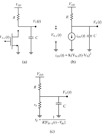
first it is assumed that all transistors are all in the saturation region. This is a common assumption in all the presented methods for representing the frequency of an RO. The proposed method is general enough to be applied on any structures but in this paper it is focused on an N-stage single-ended ring oscillator with common source stages. More complete equations for the other types of ring oscillator can be developed with the same analysis procedure. Assuming saturation for transistors, the differential equation of the circuit is obtained by a Kirchhoff’s Current Law (KCL) at each drain node (Fig. 1(a)). Fig. 3 shows one common source stage of an RO with a resistor load and the currents used in mentioned KCL equation.
Equations (12) and (13) represent a nonlinear N-dimensional differential system. The effect of parasitic capacitors that are shown in Fig. 2 is written as (14) for more accurate estimation. Pure sinusoid waveform as (15) for the outputs is the key simplifying assumption that leads to straightforward analysis along with accurate results. Assuming this, the analysis is devoted to find amplitude, A, DC level, B, and frequency, ω. Although the output of an RO will not be purely sinusoidal, the frequency representation of a practical RO output shows that it is a reasonable assumption [2], [8].
2
1 1
1
2
2 2
2 1
2 1
: ( ) 0
: ( ) 0
: ( ) 0
DD
N th
DD
th
N DD N
N N th
V V dV
node C K V V
R dt
V V dV
node C K V V
R dt
V V dV
node C K V V
R dt −
−
⎧ + + − =
⎪ ⎪
−
⎪ + + − =
⎪ ⎨ ⎪ ⎪
−
⎪ + + − =
⎪⎩
M
(12)
1
( ) 2 n ox
W
K C
L
= µ (13)
L gdp gdn dbp dbn
C=C +C +C +C +C (14)
( ) cos
o
V t = +B A ωt (15)
The phase relation among the outputs of an N-stage RO is shown in Fig. 4. Assuming equation for V2(t) as
(15), the output of the first stage can be written as (16) considering the phase relations in Fig. 4.
1( ) 2( ( ))
2 2
( 1)
cos( )
T T
V t V t
N N
B A t
N
= + −
−
= + ω + π (16)
Using a bit mathematical operations, equation (12), (15) and (16) can be combined and reduced to (17); the basic trigonometric equation of the proposed method.
(1 )
2 (1 cos( ))
(1 )
SS
jn n L gdp
mjn DD
n
jswn n
SW n gdon
mjswn DD
swn
jp p jswp n
I f
C Ad
C C
V pb
C Pd
NV W C
V N
pb
C Ad C Pd
π
=
⎡ + + + ⎤
⎢ ⎥
⎢ + ⎥
⎢ ⎥
⎢ ⎥
⎢ ⎥
× + + +
⎢ + ⎥
⎢ ⎥
⎢ ⎥
⎢ + ⎥
⎢ ⎥
⎣ ⎦
Fig. 3. Definition of currents for KCL in a delay stage.
Fig. 4. Phase relation between waveforms.
2 cos
sin
( 1)
( cos( ) ) 0
DD
B A t V
CA t
R
N
K B A t V
th N
+ − − +
−
+ + − =
ω ω ω
π
ω (17)
Equation (17) holds for every time especially for three special times mentioned in (18) that leave three beneficial equations in (19).
) sin 1 , cos 0 ) sin 0 , cos 1 ) sin 0 , cos 1
I t t
II t t
III t t
= − =
= =
= = −
ω ω
ω ω
ω ω
(18)
2
2
2
) ( sin ) 0
) ( cos ) 0
) ( cos ) 0
DD
th
DD
th
DD
th
B V
I CA K B A V
R N
B A V
II K B A V
R N
B A V
III K B A V
R N
−
⎧ + + − − =
⎪ ⎪
+ −
⎪ + − − =
⎨ ⎪
⎪ − − + + − =
⎪ ⎩
π ω
π
π
(19)
With simple calculations, the unknowns of (19) can be obtained. At the first step, the DC level of the output is obtained in term of circuit parameters as (20)
explicitly. The amplitude is obtained in term of B and other parameters as (21). Knowing the B and A, the unknown frequency of oscillation is written as (22).
1
2 cos
B V th
RK N
= + π
(20)
2
2
( )
cos ( / )
DD
th
V B
K B V R
A
K N
− − −
=
π (21)
2
( sin( / ) )
2 DD
th
B V
K B A N V
R f
CA
− + − −
= π
π (22)
These closed-form equations can represent the frequency, amplitude and DC level of an N-stage single- ended ring oscillator just knowing the circuit parameters. Equation (21) shows that the amplitude is just proportional to the circuit parameters except capacitors. Also the frequency is inversely proportional to the C and R in (22). Note that the assumptions here are the output waveform is like a sinusoid and the transistors are all in saturation region. To verify the analysis above the following two conditions should be met.
I. The transistors should not meet triode region that meansVn−1( )t <V tn( )−Vth.
II. The transistors should not meet cutoff region that meansB− ≥A Vth.
Defining the voltage across the Gate-Drain junction in first delay stage as (23), if the first condition is satisfied, the transistors remain in saturation region. Using the maximum points as an additional condition, the expression (23) is reduced to (25). So expression (25) must be satisfied for using the proposed equations. Otherwise, transistors experience the cutoff or triode regions, so a more general analysis should be performed.
1 2
( 1)
( ) ( ) [cos( ) cos ]
(1 1) ( 1)
2 sin sin
2 2
( 1) ( 1)
2 sin( )sin( )
2 2
N
V t V t A t t
N N
t t t t
N N
A
N N
A t
N N
−
− = + −
− −
+ + + −
= −
− −
= − +
π
ω ω
π π
ω ω ω ω
π π
ω
(23)
1 2
( 1)
max{ ( ) ( )} 2 sin( ) 2 cos
2 2
N
V t V t A A
N N
−
− = π = π (24)
2 cos( /A π N)<Vth (25)
3.2 Analytical Equations for The Case that Transistors Enter Triode region
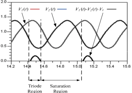
Closed-form equations for the cases that transistors meet the triode or cutoff region can be easily obtained with the same analysis. Fig. 5 illustrates the sample output voltages when the transistors meet both triode and saturation region during an oscillation period. This plot gives the evidence that the output voltage of an RO can be assumed as a sinusoid waveform if transistors meet the triode region yet. All the published methods for estimating the frequency of an RO have not represented the acceptable accuracy for the cases that the operating region changes while this paper presents closed-form equations for both amplitude and frequency of the transistors meeting all operating regions.
The analysis proposed here is again based on the KCL equations at the output of each delay stage. These equations can be written as (26).
1
2
1 1
2 2
( ) 0
( ) 0
( ) 0
N
DD
D
DD
D
N DD N
D
V V dV
C i t
R dt
V V dV
C i t
R dt
V V dV
C i t
R dt − ⎧ + + = ⎪ ⎪ − ⎪ + + = ⎪ ⎨ ⎪ ⎪ − ⎪ + + = ⎪⎩ M (26)
where iDk(t) is the Drain current of transistor number K. The output voltage is assumed sinusoid waveform as (15) to make the problem traceable. For instance, the output of the second stage is considered as (15), so the first stage output is written as (16). The unknowns here are the frequency of oscillation, the output voltage amplitude and DC level of output that are f, A and B respectively. Considering the quadratic law between Drain current and the Gate-Source voltage for the second transistor, M2, the Drain current is written as
(27) for second stage. As shown in Fig. 5, the outputs are sinusoid-like waveform yet, but the frequency of these outputs cannot be obtained from any of presented expressions. Also, there is no analysis to estimate the amplitude of the output waveform. In this section, each transistor may meet the both triode and saturation regions during one period of oscillation, so the equation for Drain current of second stage is written as (27) that is shown in bottom of this page. Substituting (26)-(27), the N-dimensional equations are obtained. Solving the obtained equations using analytical rules is difficult, so the critical points are considered to make the problem traceable. Choosing these critical points is based on having knowledge about the times when transistors are exactly in the triode or saturation region. For example, for the times ωt = 0, the output V2(t) is at maximum as it
is shown in Fig. 5, so the transistor M2 is exactly in
saturation region. The equations resulted from some
critical points is written as (28)—(30) which are at the bottom of the next page. There are just two unknowns in both algebraic equations (28) and (29). Hence, the DC level, B, and the amplitude, A, are obtained using a simple numerical solution method. Using the obtained amplitude and DC level from (28) and (29) in (30), a closed-form equation for frequency of oscillation is written as (31). This expression is shown at the bottom of the next page.
Fig. 5. Sample output voltages for the case that transistors
meet both triode and saturation regions during oscillation.
( )= 2 t iD (27) (28) (29) (30) 2 1 2 2 1 2 cos sin 1
2 {[ cos( ) ]( cos )
( cos )
} 0 for ( ) ( )
2
cos
sin
1
( cos( ) ) 0
for ( ) ( )
DD th th DD th th
B A t V
CA t
R
N
K B A t V B A t
N
B A t
V t V t V
B A t V
CA t
R
N
K B A t V
N
V t V t V
ω ω ω
ω π ω
ω
ω ω ω
ω π + − ⎧ − ⎪ ⎪ − + + + − + ⎪ ⎪ +
⎪− = > +
⎪⎪ ⎨ + − ⎪ − ⎪ ⎪ − + + + − = ⎪
⎪ < +
⎪ ⎪⎩ 2 2 ( ) ( )
2 {[ cos( ) ]( ) } 0
2
DD
th
B A V t V t is minimum
R B A
K B A V B A
N ω π π − − = ⇒ ⇒ − + + − − − = 1 2 ( ) cos( ) sin( ) 2
( cos( ) ) 0
DD
th
t V t is minimum N
B A V
N CA
R N
K B A V
N π ω π π ω π = − ⇒ ⇒ + − + + − − = ( ) 2 2 0
( cos( ) ) 0
t
DD
th
t V is maximum
B A V
K B A V
R N
ω
π
= ⇒ ⇒
+ − + + − =
(31)
3.3 Analytical Equations for The Case that
Transistors Enter Cut-Off region
Each transistor of an RO experiences the cut-off region in a period of oscillation if the loop gain increases. This occurs when the expression (32) is not satisfied.
th
V A
B− ≤ (32) where A, B are obtained by solution of (28) and (29). Fig. 6 shows a period of oscillation in the case that the expression (32) is not satisfied. This plot shows the all operating regions that a transistor may enter under this condition. Fig. 7 shows the circuit model for a delay stage while each state occurring. At the beginning of the period, transistor is off because of the low voltage at its gate connection, so the circuit is modeled as an RC circuit with a time constant. The transistor meets the saturation region when the voltage at the Gate connection overcomes the threshold voltage, Vth. In this
state, the transistor can be modeled as a voltage controlled current source (VCCS) and increasing the gate voltage increases the current and causes the charge of the capacitor decreases. If the Drain-Gate voltage of the transistor becomes higher than threshold voltage, Vth, transistor experiences deep triode and triode region
respectively.
Here, the transistor can be modeled as a small voltage controlled resistor that is parallel with load resistor, R, so the output voltage decreases with a small time constant because of small load resistor. Calculating the all break points and time constants is more difficult and not necessary for the case.
A simple method based on a novel approximation is proposed here. Because of short times in each period that transistors are in saturation and deep triode, it can be assumed that transistors are only in triode and cutoff. Hence, the output voltage is assumed as a triangular-like periodic waveform. The output voltage at each stage is written as (33).
⎩ ⎨ ⎧
< <
< < −
= −
T t t
t t e
V t V
m m RC
t DD N
for 0
0 for ) 1
( ) (
/
(33) Fig. 8 shows sample waveforms and the estimated waveform for a three stage RO under this condition. Because of the phase relation between outputs, each transistor can experience the off region for only T/N of time at the end of each period. Hence, the unknown parameters, tm, Vm, that are shown in Fig. 8 can be easily
obtained. Equation (33) can be written for V2(t) at the
time tm as (34) and because of the phase relation, the
output V1(t) is written as (35).
Fig. 6. A period of oscillation of output voltage for the case
that the transistors experience all possible regions.
(a) (b)
1
1
[ ( ) ] d
N th
r
K V − t V
=
−
(c)
Fig. 7. Circuit models for each state occur in Fig.. 6. a)
transistor off b) transistor is in saturation c) triode and deep triode region
Fig. 8. A period of oscillation of output voltage for the case
that transistors meet all regions. 2
2
cos( ) ( cos( ) )
2 sin( )
DD th
B A V RK B A V
N N
f
RCA N
π π
π π
+ − + − −
=
) 1
( )
( /
2
RC t DD m
m
e V t
V = − − (34)
)
1
(
)
/
(
)
(
2 ( / )/1
RC N T t DD
m
e
V
N
T
t
V
t
V
=
−
=
−
− − (35)An additional condition here is the voltage at gate-drain junction must satisfy (36) for edge of triode region. This condition occurs at time tm referring (37), (38) and Fig. 8. Substituting (34)-(37) the unknown parameters can be defined as a function of T. Therefore, the only unknown parameter after all is period of output waveform, T.
2( )m 1( )m th
V t −V t =V (36)
( )/
/
[1 m ] [1 m ]
T
t RC
t RC N
DD DD th
V −e− −V −e− − =V (37)
/ 1
( T NRC )
DD m
th
V e
t RCLn
V
−
= (38)
The same expression can be used for V1(t) at the
time T as (39)-(40). Substituting (38)-(41) result in an equation for the period of time, T, as (42).
1 2 2
( 1)
( ) ( / ) [ ] m
N
V T V T T N V T V
N
−
= − = = (39)
/ 1
2( ) ( 1)
T NRC
m m DD th
V =V t =V −V e − − (40)
1 [1 exp( . )]
DD m
N T
V V
N RC
−
− − = (41)
ln( )
1
DD
DD m
N V
T RC
N V V
=
− − (42)
4 Simulation Versus Analytical Results
To evaluate the proposed method and compare with competitive methods, a test benchmark is created in this section using Advanced Design System software. The TSMC 1.8 V, 0.18 µm CMOS process have been used in simulations. Table 3 gives the details of technology, supply voltage, load capacitor, size and threshold voltages of the transistors used in simulations. First, a single-ended ring oscillator is simulated using different values of load capacitor for different oscillation frequencies. The sizes of the transistors were chosen here such that the circuit would oscillate over a wide range of capacitor. Different size of transistors is chosen to obtain all possible conditions in each experiment because of the direct relation between the amplitude of outputs and the loop gain. Higher loop gain causes higher amplitude; consequently more nonlinear behavior and different waveforms are available. Due to
this, the size of the devices is changed in a wide range to test the circuit in different scenarios. For instance, the smaller transistor results in the smaller loop gain so that the outputs are fine sinusoid wave forms. The frequency is plotted as a function of CL in this case. Second
experiment is performed while the both number of delay stages and the sizes of the transistors are changed. In the third experiment, the amplitude and the frequency of oscillation are measured while load resistor is varied under simulation steps. These simulations are repeated for the cases that transistors change the operation region. The devices are larger to have more amplitude, so the change of operation regions is guaranteed in each scenario.
Table 2. Comparison between simulation results and
calculated unknown parameters when devices enter the cutoff region
Simulation results Calculated values
Load Capacitor
CL (pF) Period (T)
(nsec)
tm (nsec)
Period (T) (nsec)
tm (nsec)
1 1.11 0.63 0.90 0.58
2 1.22 0.71 1.13 0.70
3 1.43 0.82 1.36 0.84
4 1.65 0.93 1.58 0.97
5 1.81 1.02 1.80 1.11
6 1.96 1.10 2.03 1.24
7 2.15 1.20 2.26 1.38
8 2.30 1.30 2.48 1.50
9 2.44 1.40 2.69 1.65
10 2.59 1.63 2.92 1.80
Peak Voltage
(Vm)
1.12 Volts 1.4 Volts
Table 3. Details of Technology, Supply Voltage, Load Capacitor Range, Size and Threshold Voltages of Transistors
Technology TSMC 0.18 µm
Supply Voltage 1.8 V
Lmin 0.18 µm
µn.Cox 275.6×10⁻⁶ F/(V.s)
Capacitor (max/min) 10 pF / 1 pF
Size for Saturation (W/L) 50
Size for Triode (W/L) 80
Size for Cut-off (W/L) 300
VTN (normal/low) 0.47 V / 0.267 V
VTP (normal/low) -0.46 V / -0.37 V
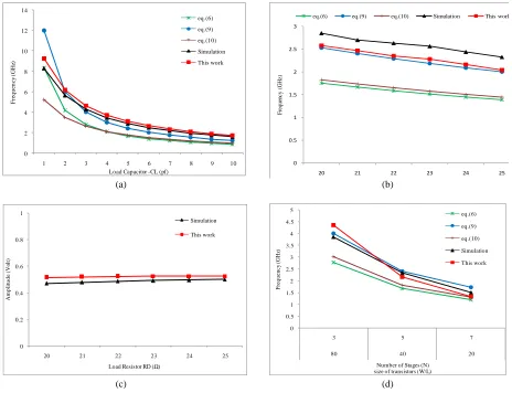
The calculated frequency by the proposed equations, (20), (21) and (22) when transistors are in the saturation region are compared with the simulation results
obtained by the other methods. These comparisons are illustrated in Fig. 9 which shows the accuracy of proposed method. The equation that has been presented in [12] is inaccurate and it was eliminated from the results to have better comparison. Fig. 10 illustrates the simulation results compared with analytical equations (28), (29) and (31) for the case that the transistors meet both saturation and triode region during oscillation. A numerical method using MATLAB software is used to solve the equations (28) and (30) to obtain the amplitude and DC level of output. For the case that transistors enter the cutoff region, Fig. 11 shows the simulation results and the estimated output waveform of
one stage. The unknown parameters of the estimated output are calculated by equations (38), (39), (43). Estimated results and actual values undergoes the variation of output capacitance are given in Table 2. In this experiment, the unknown parameters of the estimated outputs are calculated by equations (38), (39), (43) and a comparison between estimated and real values shows the accuracy of analytical equations. Based on the presented plots, it is evident that the equations proposed in this paper appear to be more accurate for all simulations in comparison with the others.
0 1 2 3 4 5 6 7 8 9 10 11 12 13
1 2 3 4 5 6 7 8 9 10
F
re
que
nc
y (
G
H
z)
Load Capacitor CL (pf) eq.(6)
eq.(9)
eq.(10)
Simulation
This work
2 2.5 3 3.5 4 4.5 5 5.5 6 6.5 7
21 22 23 24 25 26
F
re
que
n
c
y
(
G
H
z)
Load Resistor RD (Ω)
eq.(6) eq.(9) eq.(10) Simulation This work
(a) (b)
0 0.1 0.2 0.3 0.4 0.5 0.6 0.7 0.8 0.9 1
1 2 3 4 5 6
A
m
p
litu
d
e (
V
ol
t)
Load Resistor RD (Ω)
Simulation
This work
1 1.5 2 2.5 3 3.5 4 4.5
3 5 7
50 15 12
F
re
q
ue
nc
y
(
G
Hz
)
Number of Stages (N) Transistors Sizes (W/L)
eq.(6)
eq.(9)
eq.(10)
simulation
This work
(c) (d)
Fig. 9. Comparison of simulation and analysis results when transistors are in saturation region.
(a) Frequency versus CL (b) Frequency versus RD (c) Amplitude versus RD (d) Frequency versus (N, W/L)
5 Conclusion
This paper has presented a novel method to derive exact analytical equations for the amplitude and frequency of ring oscillators. The output signal is assumed a sinusoidal waveform where the unknowns are amplitude, frequency and DC level. Applying the large signal analysis, the equations derived in this paper represent both amplitude and frequency more accurately than previous equations for a ring oscillator. Nonlinear behavior of an oscillator can be explained easily with
the presented equations. Also, the equations are provided for all operation regions of transistors but the effect of channel length modulation and more parasitic element are challenging points that limits the analysis. These equations will be of significant to be used in guiding ring oscillator design. It also can provide designers more insight not only into design methodology, but also for estimating the phase noise, injection locking, etc; future works one may perform.
0 2 4 6 8 10 12 14
1 2 3 4 5 6 7 8 9 10
F
re
que
nc
y
(
G
H
z)
Load Capacitor -CL (pf)
eq.(6)
eq.(9)
eq.(10)
Simulation
This work
0 0.5 1 1.5 2 2.5 3
20 21 22 23 24 25
Fr
eq
ue
nc
y (
G
H
z)
eq.(6) eq.(9) eq.(10) Simulation This work
(a) (b)
0 0.2 0.4 0.6 0.8 1
20 21 22 23 24 25
A
m
p
litu
d
e
(
V
o
lt)
Load Resistor RD (Ω)
Simulation
This work
0 0.5 1 1.5 2 2.5 3 3.5 4 4.5 5
3 5 7
80 40 20
F
re
q
ue
nc
y (
G
H
z)
Number of Stages (N) size of transistors (W/L)
eq.(6)
eq.(9)
eq.(10)
Simulation
This work
(c) (d)
Fig. 10. Comparison of simulation and analysis results when transistors meet the triode region
(a) Frequency versus CL (b) Frequency versus (N, W/L) (c) Amplitude versus RD (d) Frequency versus RD
3.
00 3.05 3.10 3.15 3.20 3.25 3.30 3.35 3.40 3.45 3.50 3.55 603. 3.65 3.70 3.75 3.80 3.85 903. 3.95 4.00 4.05 4.10 4.15 4.20
2.
95 4.25
0.2 0.4 0.6 0.8 1.0 1.2 1.4
0.0 1.5
time (nsec)
out
put
vol
ta
ge
(V
ol
t)
Estimated Waveform Simulation Output
Fig. 11. Sample output voltage of an RO and the estimated
waveform for the case that transistors meet cut-off region.
References
[1] Hesieh Y.B. and Kao Y.H., "A Fully integrated spread-spectrum clock generator by using direct VCO modulation," IEEE Trans. Circuit Syst. I, Regular Papers, Vol. 55, pp. 1845-1853, August 2008.
[2] Anand S. S.B. and Razavi B., "A CMOS clock recovery circuit for 2.5-Gb/s NRZ data," IEEE J.
Solid-State Circuit, Vol. 36, pp. 432–439, March 2001.
[3] Savoj J. and Razavi B., "A 10 Gb/s CMOS clock and data recovery circuit with a half-rate linear phase detector," IEEE J. Solid-State Circuit, Vol. 36, pp. 761–768, May 2001.
[4] Razavi B., "A 2-GHz 1.6-mW phase-locked loop," IEEE J. Solid-State Circuits, Vol. 32, pp. 730–735, May 1997.
[5] Sun L. and Kwasniewski T. A., "A 1.25-GHz 0.35-µm monolithic CMOS PLL based on a multiphase ring oscillator," IEEE J. Solid-State Circuits, Vol. 36, pp. 910–916, June 2001.
[6] Srivastava S. and Roychowdhury J., "Analytical equations for nonlinear phase errors and jitter in ring oscillators," IEEE Trans. Circuits Syst. I, Regular Papers, Vol. 54, pp. 2321-2329, October 2007.
[7] Mollah A.K.M.K., Rosales R., Tabatabaei S., Cicalo J. and Ivanov A., "Design of a tunable differential ring oscillator with short start-up and switching transients," IEEE Trans. Circuit Syst. I, Vol. 54, pp. 2669-2682, December 2008.
[8] Hegazi E., Rael J. and Abidi A., The Designer’s Guide to High-Purity Oscillators. United States of America: Kluwer, 2005, Chapter 1.
[9] Pichler M., Stelzer A., Gulden P., Seisenberger C. and Vossiek M., "Phase-Error measurement and compensation in PLL frequency synthesizers for FMCW sensors- II: Theory," IEEE Trans. Circuit Syst. I, Vol. 54, pp. 1224-1235, June 2007.
[10] Hajimiri A., Limotyrakis S. and Lee T.H., "Jitter and phase noise in ring oscillators," IEEE J. Solid-State Circuit, Vol. 34, pp. 790–804, June 1999. [11] Razavi B., "A study of phase noise in CMOS
oscillators," IEEE J. Solid-State Circuits, Vol. 31, pp. 331–343, Mar. 1996.
[12] Razavi B., Design of Analog CMOS Integrated Circuits. New York: McGraw Hill, 2001, Chapter 14.
[13] Weigandt T., "Low-phase-noise, low-timing-jitter design techniques for delay cell based VCOs and frequency synthesizers," Ph.D. dissertation, Univ. California, Berkeley, 1998.
[14] Leung B., VLSI for Wireless Communication. Upper Saddle River, NJ: Prentice-Hall, 2002. [15] Alioto M. and Palumbo G., "Oscillation frequency
in CML and ESCL ring oscillators," IEEE Trans. Circuits Syst. I, Vol. 48, pp. 210–214, Feb. 2001. [16] Docking S. and Sachdev M., "A method to drive an
equation for the oscillation frequency of a ring oscillators," IEEE Trans. Circuits Syst. I, Vol. 50, pp. 259–264, Feb. 2003.
Payam. M. Farahabadi received the
B.Sc degree in electrical and computer engineering from University of Mazandaran, Babol, Iran, in 2006. He is currently pursuing M.Sc student in electronic engineering at Babol University of Technology, Babol, Mazandaran, Iran. He is currently with the Integrated Circuits Research Laboratory, Babol University of Technology. His research interest includes CMOS RF circuits for wireless communications, high frequency low phase noise oscillators, mixed analog-digital integrated circuits focus on phase locked loops, monolithic clock and data recovery circuits, Kalman filtering focus on frequency estimation techniques.
Hossein Miar-Naimi received the B.Sc.
from Sharif University of Technology in 1994 and M.Sc. from Tarbiat Modares University in 1996 and Ph.D. from Iran University of Science and Technology in 2002 respectively. Since 2003 He has been member of Electrical and Electronics Engineering Faculty of Babol University of Technology. His research interests are analog CMOS integrated circuit design, RF microelectronics, Image processing and Evolutional Algorithm.
Ataollah Ebrahimzadeh received the
B.Sc. from University of Tehran in 1995 and M.Sc. from Amirkabir University of Technology in 1999 and Ph.D. from Ferdowsi University of Mashad in 2006 respectively. Since 2006 He has been member of Electrical and Electronics Engineering Faculty of Babol University of Technology. His research interests is digital signal-type identification and classification.