ScholarWorks@UNO
ScholarWorks@UNO
University of New Orleans Theses and
Dissertations Dissertations and Theses
5-21-2004
Influence of Underfill on Ball Grid Array (BGA) Package Fatigue
Influence of Underfill on Ball Grid Array (BGA) Package Fatigue
Life
Life
Geetha Chilakamarthi University of New Orleans
Follow this and additional works at: https://scholarworks.uno.edu/td
Recommended Citation Recommended Citation
Chilakamarthi, Geetha, "Influence of Underfill on Ball Grid Array (BGA) Package Fatigue Life" (2004). University of New Orleans Theses and Dissertations. 85.
https://scholarworks.uno.edu/td/85
This Thesis is protected by copyright and/or related rights. It has been brought to you by ScholarWorks@UNO with permission from the rights-holder(s). You are free to use this Thesis in any way that is permitted by the copyright and related rights legislation that applies to your use. For other uses you need to obtain permission from the rights-holder(s) directly, unless additional rights are indicated by a Creative Commons license in the record and/or on the work itself.
A Thesis
Submitted to the Graduate Faculty of the University of New Orleans in partial fulfillment of the requirements for the degree of
Master of Science in
The Department of Mechanical Engineering
by
Geetha Chilakamarthi
ii
Acknowledgement
I would like to thank Dr. Melody Arthur Verges, my major professor, and my mentor for her sincere guidance, help, and giving me a chance to do this project. Without her, this would have been impossible.
I am grateful to Dr. Paul D. Schilling and Dr. Paul D. Herrington for serving on my graduate committee.
Furthermore, I would like to thank all the people that have helped and encouraged me in completing this work: my parents, Bhanu Prasad, Vijaya Lakshmi, my sister Sandhya, and my friend Nelson Akafuah who provided inspiration and support when needed.
Finally, I would like to acknowledge Jesus Christ. Since coming to know Him, my life has never been the same. He has transformed me emotionally and spiritually and to Him I give glory. I like to finish my acknowledgement with one of my favorite Bible verses:
Philippians 3:12-14 “Not that I have already obtained all this, or have already been made perfect, but I press on to take hold of that for which Christ Jesus took hold of me. I do not
iii
Dedication
I dedicate this project to my parents, who have provided me with support emotionally and financially throughout this long journey called my college career, and to Ratan, my greatest emotional and spiritual support. He continuously encouraged me, prayed for me and patiently stood by my side. I thank God for the rest of my family, who supported me with their prayers and encouraging words.
iv
TABLE OF CONTENTS
List of Figures ...v
Abstract... vii
1. Introduction...1
2. Literature Review ...6
2.1 Basic Fatigue Life Approaches...6
2.2 Fatigue Life of Solder connections ...9
2.3 Fracture Model for Solder connections...11
3. Finite Element Model ...15
3.1 Finite Element Geometry...16
3.2 Boundary Conditions ...17
3.3 Material Constituents...19
3.4 Thermal Loading...20
3.5 Convergence Criterion...21
4. Results ...24
4.1 Influence of Underfill Parameters...25
4.2 Significance of Mode I Cyclic Stresses ...30
4.3 Comparison of Mode I Cyclic Stresses with Mode II Cyclic Stresses ...37
5. Conclusions and Recommendations...40
References...42
Appendix A...44
Appendix B ...47
v
List of Figures
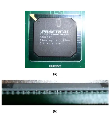
Figure 1.1(a) Picture showing top view of BGA package...2
Figure 1.1(b) Picture showing side view of BGA package...2
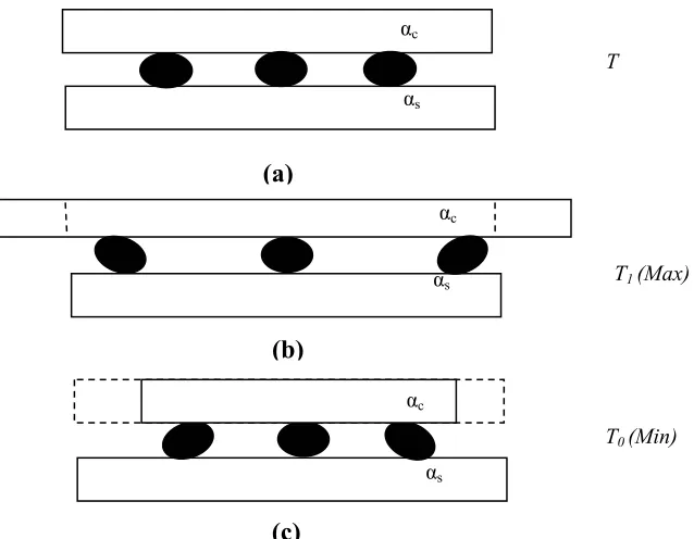
Figure1.2 Schematic of row of interconnects subjected to thermal cycling
(a) The shape of interconnects at some reference temperature T (b) Deformed shape of interconnects at some maximum temperature T1 (c) Deformed shape of
interconnects at some minimum temperature T0 ...4
Figure 1.3 Schematic showing the crack prone areas in the solder ...4
Figure 2.1 The three types of loading that can be experienced by a crack ...8
Figure 2.2 Schematic depicting stresses on an edge crack. (a) Mode II shear stress. (b) Shear stress with an additional compressive Mode I stress. (c)
Shear stress with an additional tensile Mode I stress...12
Figure 3.1 A three dimensional view of a unit cell. The inner cylinder is representative of the solder connection while the outer cylinder is representative of the
underfill...15
Figure 3.2(a) Three-dimensional view of the unit cell with a highlighted section showing
the cross-sectional view of the finite element geometry...17
Figure 3.2(b) Two dimensional geometry used in the creation of the axisymmetric finite
element model...17
Figure 3.3 Schematic of finite element geometry with the dimensions and boundary
conditions...19
Figure 3.4 Ansys plot showing the mesh of finite element geometry ...22
Figure 3.5 Graph depicting the convergence criterion for normal stress values along the top boundary of the solder interconnection. The underfill material properties for this case Eu=3.5GPa, νu=0.3, and αu=100X10-6/K. The
vi
Figure 4.1 Graph depicting normal stress values along the top boundary of the solder interconnection. The underfill properties for this case are Eu=3.5GPa, νu=0.3,
and αu= 100x10-6/K. The temperature loading is from 25°C to 5°C ...25
Figure 4.2 Graphs depicting the normal stresses at the nodes located at the middle of the solder interconnect (a)Eu=2.0GPa (b)Eu=3.5GPa (c)Eu=5.0GPa
(d) Eu=6.5GPa (e) Eu=8.0GPa...26
Figure 4.3 Schematic of the fluctuation of normal stresses over a temperature cycle for the case of Eu=2.0GPa and νu=0.3 assuming temperature profile is
sinusoidal (a) αu=10x10-6/K (b) αu=40x10-6/K (c) αu=70x10-6/K (d) αu=100x10 -6/K ...29
Figure 4.4 Schematic showing the addition of Mode I cyclic stresses to steady state
stresses ...31
Figure 4.5 Graphs depicting the most tensile stresses induced in the solder during one thermal cycle when temperature is 5°C and %sh of underfill material is 0.6 (a) Eu=2.0GPa (b) Eu=3.5GPa (c) Eu=5.0GPa (d) Eu=6.5GPa
(e) Eu=8.0GPa ...32
Figure 4.6 Plot depicting the normal stresses for the case when νu = νs and αu =αs...35
Figure 4.7 Graph depicting the normal stress values for real underfill material properties....36
Figure 4.8 Schematic of sinusoidal plot of Mode I stresses for real underfill material
properties...37
Figure 4.9 Schematic of top view of a ten by ten array of solder interconnects in BGA package (the numbered joints represents the joints for which shear stress is
vii
Abstract
The influence of underfill material properties on the fatigue life of Ball Grid Array (BGA) packages that are subjected to thermal cycling is investigated in this study. A finite element model is created using Ansys by assuming the existence of an infinite array of solder interconnects, cylindrical in shape, surrounded by underfill material. Axial stresses in the interconnects are determined as a temperature loading is applied. The results show that these normal stresses are on the same order of magnitude as the hydrostatic compressive stresses induced in the solder upon underfill curing. Therefore it is concluded that for the range of
1. Introduction
The rapid improvement in the electronic industry across a wide range of sectors including aerospace and automotive, are dependent on the structural integrity of embedded
micro-electronic components and assemblies. Solder joints were initially intended to be simple
electrical interconnections between mechanically interlocked components in electronic packages. However, as with any new technology, the size of electronic components have been decreasing while the number of input/output terminations have been increasing. As a result, the number of solder joint connections have increased while the dimensions of joint have decreased. Moreover, packaging engineers are interested in incorporating even smaller solder joints as the need
increases for designing packages with more performance options. Several packaging
1. Chip Carrier
2. Printed Circuit Board (PCB) 3. Solder Interconnect
(a)
(b)
Figure 1.1 Picture of the BGA package. The top component is the integrated circuit chip. The bottom component is the printed circuit board. (a) Top view of package. (b) Side view of package.
disc, sphere etc. which contain flux as an inner core. The solder paste is actually a suspension of solder particles in a cream flux. The additives are included in the cream flux to promote wetting and control paste properties. Generally solder paste is applied to the metallizations on the PCB using a screen printing or stencil operation Once the paste is applied to the circuit board, the components are usually positioned on the board and held there by the tackiness of the paste. This package is then ‘reflowed’ in an oven, or some other heating mechanism, so that the joints are formed [Frear et.al, (1994)].
The reliability of solder joints is one of the critical issues in surface mount technology. A key issue in long term reliability of solder joints is joint failure during thermal cycling. The individual components that are soldered together in an electronic package typically have different thermal expansion coefficients. When this package is subjected to a thermal loading, the interconnects undergo shear as a result of a mismatch of coefficient of thermal expansion between the chip carrier and the PCB. If, for example, the coefficient of thermal expansion of the chip is greater than that of PCB, the chip carrier will expand more than the PCB. Figure 1.2 shows a schematic of a row of interconnects subjected to thermal loading. Figure 1.2 (a) depicts the shape of interconnects at some reference temperature, T. Figure 1.2 (b) depicts the deformed shape of interconnects at some maximum temperature, T1. Finally, Figure 1.2 (c) shows the
deformed shape of the interconnects at some minimum temperature, T0. As the distance between
the interconnect and neutral point of package increases, the shearing stresses at solder joints also increases in magnitude. Hence this shear stress induces Mode II loading which leads to
Figure 1.2 Schematic of row of interconnects subjected to thermal cycling. (a)The shape of interconnects at some reference temperature, T. (b) The deformed shape of interconnects at some maximum temperature, T1. (c) The
deformed shape of interconnects at some minimum temperature, T0.
Figure 1.3 Schematic showing the crack prone areas in the solder.
While many researchers have investigated this Mode II shearing of solder joints, Mode I loading can be introduced by several factors including warpage, a mechanical constraint, or the presence of underfill. Underfills are typically polymeric adhesives with a glass transition temperature in the neighborhood of 125°C and act elastically at room temperature. Underfill is usually dispensed as a drop of liquid to fill the volume between the solder interconnects. The liquid is allowed to wick between the package and PCB which subsequently cures to a solid.
αc αc
αc
αs αs αs
(a)
(b)
(c)
T
T1 (Max)
Most commonly used underfills exhibit unconstrained shrinkage of up to 3% or more in volume. This contraction that tends to pull the package closer to PCB, is limited by the presence of solder interconnects thus inducing compression in the interconnects in axial direction. The primary purpose of an underfill is to reduce the solder strain by mechanically coupling the die and the PCB. Hence the presence of underfill acts to prolong the fatigue life of BGA package.
While several researchers have focused on the development of the compressive hydrostatic stresses in the solder as a result of underfill curing, the primary goal of this work deals with investigating the significance of axial (Mode I) cyclic stresses that may be induced in the presence of thermal cycling. Hence a finite element model of the solder in the underfill material is developed using Ansys. The following chapter presents the current fatigue life models and discusses thermal cycling effects in a BGA package. Chapter 3 deals with the detailed
2. Literature Review
As mentioned in the introduction, thermal cycling tests are generally used in electronic packaging industry to predict the reliability and thermal fatigue failure in solder joints [Kaga et.al, (1999)]. When an electronic package is subjected to thermal cycling, the solder
interconnects experience shear due to thermal expansion mismatch loading and hence causes the crack to initiate and propagate in the solder. This chapter discusses the thermal cycling effects which induces Mode II shear, the effect of underfill which induces Mode I compressive force to inhibit the crack growth, as well as a literature review of various fatigue life models.
2.1 Basic Fatigue Life Approaches
For over a century, researchers have proposed different life prediction techniques for determining fatigue life. Fatigue life models can generally fall into three different approaches: (a) the strain-based approach, (b) the energy-based approach, and (c) the fracture-based approach.
Strain approach
joint. The fatigue life of the most of the solders which experience shear strain can be predicted using this strain based approach.
The simple power law equation proposed by Coffin-Manson which relates the plastic strain,∆γ p, to the fatigue life is given by
(Nf )α ∆γ p = Ө (1)
where Nf is the fatigue life, α is the fatigue ductility exponent and Ө is the fatigue ductility
coefficient. The slope of log-log curve between number of cycles required to failure and plastic strain determines the fatigue ductility exponent.
Energy approach
The energy-based approach for fatigue life prediction relates the mechanical hysteresis energy,
W, with the number of cycles to failure. Morrow (1965) was one of the first modern fatigue researchers to show that fatigue life could be correlated with the mechanical energy of the hysterisis loop. This method recognizes that stress is required to move the dislocations required for irreversible local plastic deformation. Nearly all of the energy which is imparted goes in to heat whereas a fraction of this energy is assumed to damage the material which results in failure of the joint. Hence energy approach can be expressed as
Nfm W = ӨE (2)
Where Nf is the fatigue life, W is the hysterisis energy and ӨE and m are constants.
Fracture mechanics approach
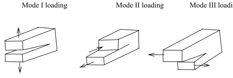
that a crack can experience: (a) Mode I loading, (b) Mode II loading, and (c) Mode III loading. A cracked body can be loaded in any of these modes or a combination of two or three modes.
Mode I loading Mode II loading Mode III loading
Figure 2.1 The three types of loading that can be experienced by a crack.
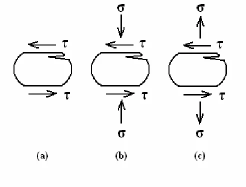
A Mode I loading is an opening or a tensile mode of loading where principal load is applied normal to the crack plane where the crack faces are pulled apart. Mode II refers to in-plane shear loading and tends to slide one crack face with respect to the other. Mode III corresponds to out-of-plane or tearing shear where the crack surfaces move parallel to the leading edge of the crack and relative to each other. Paris and Erdogan (1963) were the first to discover the power law relationship for fatigue crack growth and hence the equation is popularly known as Paris law which is described as
K C dN
da = ∆ m
(3)
where
dN da
2.2 Fatigue Life of Solder Connections
The primary concern for interconnect failure is from the resulting shear caused due to difference in thermal expansion between the chip and PWB in the presence of cyclic temperature variations. As a result the induced shear is assumed to be displacement-controlled and thus the magnitude depends upon the distance of particular interconnect from the center, or neutral point, of the array denoted as L in figure 1.2. As the temperature is increased from T to T1, assuming
α p>α c the resulting thermal or shearing displacement, ∆, of the bottom of the joint with respect
to the top is
∆= (α p- αc )( T1- T)
2
L
(4) where α p and α c are the coefficient of thermal expansion of the PCB and the chip carrier and
(L/2) is the distance of interconnect from the neutral point of the package (The neutral point is the point where there is no relative sliding displacement between the surfaces).The nominal shear stress τ can be expressed as
τ = h
∆
G =
) 1 ( 2 +υ
Ε ∆
h (5)
where h is the height of the interconnect and G is the shear modulus. The temperature change is the most common cause of solder joint cracking in electronic packages which leads to strains in solder joints due to thermal expansion mismatch between various materials resulting in fatigue failure [Nemeth et.al, (2000)]. Due to this thermal mismatch the shear strain associated with the interconnects can be expressed as:
γ =
h L
∆Τ ∆α
where ∆α is the difference between the coefficient of thermal expansion between the PWB and the chip and ∆T is the change in temperature that causes resulting strain.
Vaynman and McKeown (1991) proposed a strain energy partitioning approach for modeling the fatigue behavior and assumed that fatigue damage caused during each cycle is proportional to plastic hysterisis energy per cycle which is replaced by damage function consisting of both stress and strain rate component to predict the fatigue life of solder. In research performed by Solomon and Tolksdorf (1995), they concluded that the plastic strain governs the fatigue life.
In order to compensate for the effect of these stresses and strains during thermal fatigue, an underfill is introduced into the gaps between the solder interconnects. Sitaraman et al. (2001) tested the effect of underfill on SBGA (super ball grid array) packages. Three types of underfills were examined in this study. They observed that the properties of underfill play a vital role in reliability of BGA packages; e.g., a low coefficient of thermal expansion and high
modulus underfill significantly reduces solder strain. Hung et al. (2000) underfilled the solder joints with 15 packages of flex type BGA and tested for more than 8 months in a test chamber and found no defects in the packages. They noticed no failure in these solder joints even after 5800 cycles. Liji et al. (2002) investigated failure mechanisms and cycles to failure for two groups of PBGA (Plastic Ball Grid Array) samples both with and without underfill. It was observed that the sample with no underfill failed after 500 cycles whereas the sample with underfill survived without a crack even after 2700 cycles. This clearly shows that underfill can very well protect the solder ball and can act to increase the life of BGA package. FEM
the maximum stress without underfill was 78.4MPa. While improving the life of a solder joint using underfill it was suggested that careful attention is needed about other modes of failure like warpage etc.
Burnette et al. (2000) conducted an experiment on underfilling ceramic BGA packages using four types of epoxies with different coefficients of thermal expansion and moduli of elasticity. Their experimental results proved that the board level reliability for Ceramic Ball Grid Array packages was greatly increased by using underfill epoxy. In addition, the coefficient of thermal expansion of underfill was one of the important parameters that contributes to the reliability of packages.
2.3 Fracture Model for Solder Connections
Fracture mechanics approaches have become a beneficial tool in characterizing crack growth caused by fatigue. The most common equation used in determining the fatigue life of a cracked component or structure subjected to a single Mode of loading is the Paris law. Other researchers have modified this equation to include other parameters. For instance, Forman suggested the following relationship:
− ∆Κ = ∆Κ − − ∆Κ = − crit m crit m K K C K K K C dN da max 1 max min 1 1 (7)
where Kmax is the maximum stress intensity factor, Kmin is the minimum stress intensity factor,
and ∆K =Kmax –Kmin. This modification serves to include the fracture toughness of the material,
Kcrit, as an important parameter in determining the fatigue life. Pao (1992) developed a fatigue
importance when plasticity is present. Elber (1970) proposed a fatigue crack growth equation which is a modified form of Paris Erdogan equation and is given as
m eff C dN
da = ∆Κ
(8)
where ∆Keff ≡Kmax-Kop in which Kmax is the maximum stress intensity factor, Kop is the stress
intensity at which crack opens,
dN da
is the fatigue crack growth per cycle, and C and m are material constants determined experimentally.
When using the above equations only one Mode of loading can be considered. For example, when dealing with the thermal fatigue of solder connections, typically a Mode II cyclic loading is considered when predicting the fatigue life of the connections. As one can imagine, the addition of a tensile loading should act to grow the crack more quickly while the addition of a compressive loading should act to close the crack and therefore, inhibit it from growing as
quickly. Refer to figure 2.2. Larson and Verges (2003) developed a fracture-based fatigue life model based on this concept assuming that the Mode I component is constant.
They plotted the relative life prediction equations which show that an axial tension along with shearing decreases the fatigue life whereas the axial compression along with shearing increases the fatigue life of interconnects. Hence the equation for relative increase in the fatigue life due to axial compression was given as
+ = ) 2 ( Gr f N N µ πγ πγ (9)
where N(c) is the fatigue life when interconnect is subjected to axial compression, N(o) is the fatigue life in absence of an axial load, f is the axial force, r is the radius of the interconnect, γ is the shear strain, and µ is the friction coefficient.
In order to enhance the reliability of solder joints, a constant Mode I compressive loading can be introduced by several factors including a mechanical constraint or the presence of underfill. Most commonly used underfills exhibit unconstrained cure shrinkages of up to 3% or more in volume. This contraction that tends to pull the package closer to the printed wiring board, is limited by the presence of solder interconnects thus inducing compression in the interconnects in the axial direction. Initially, the contraction of the underfill will also cause the solder to undergo tension in the radial direction. Larson et al. (2004) modeled underfill curing in a BGA package. They concluded that after the solder is allowed to creep, the final steady state stresses are in hydrostatic compression.
Larson et al. (2004) also developed an equation using nonlinear finite element analysis to predict the steady state stresses caused by contraction of the underfill upon curing using
ABAQUS. They tested for various ranges of underfill properties (Eu=0.5 to 8.0GPa, νu=0.2 to 0.4
σs = (A (Eu /σy )+B)* %shu*Eu/ (1-νu) (10)
for estimating the influence of underfill parameters such as %shu, Eu, and νu on steady state
compressive stresses. In this equation σy is the yield stress of the solder and is taken to be 33MPa, A= 2.94x10⁻⁶, B= -2.85x10⁻³ and %shu is the linear percentage shrinkage of underfill
material.
3. Finite Element Model
A finite element model is developed to predict the influence of an underfill on the Mode I loading of an interconnect in a BGA package in the presence of thermal cycling using Ansys 7.1. The finite element geometry of the solder interconnect implemented here is the same as
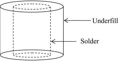
considered by Larson et al. (2004). The primary assumptions are that the solder interconnections are a part of infinite array and that the geometry of the connections has a negligible effect on the normal stresses. This second assumption allows the solder to be modeled as a cylinder. Therefore the geometry considered for the finite element model is a unit cell of two concentric cylinders. The outer cylinder represents the underfill and the inner cylinder represents the solder connection as shown in figure 3.1.
Figure 3.1 A three dimensional view of a unit cell. The inner cylinder is representative of the solder connection while the outer cylinder is representative of the underfill.
The solder modeled in the analysis is a eutectic composition of lead and tin which is commonly used in electronic packages as both mechanical and electrical connections because of its
favorable wetting property. The underfill modeled in the analysis is a polymeric adhesive which can produce a beneficial compression upon shrinkage in BGA interconnects. This finite element analysis is developed using general purpose ANSYS code which is included in Appendix A. The analysis methodologies implemented in the ANSYS software code are discussed in detail in each section of this chapter.
3.1 Finite Element Geometry
The actual finite element geometry is an axis-symmetric model of a unit cell cross section as shown in Figure 3.2. The two dimensional finite element model is constructed with 4-noded PLANE 182 axis-symmetric elements. The element selection and descritization are two
important assumptions which play a key role in finite element model. The choice of type of element used depends on the number of degrees of freedom needed to which the physical structure can be modeled without any approximation. The dimensions of the geometry are chosen such that the unit cell is representative of commonly used area array packages such as BGA’s, chip scale and flip-chip packages; i.e., the height of the interconnect is 0.5mm, the radius of the pad is 0.4mm, and the pitch (the distance between the connections) is 1.27mm. Therefore, for the cross-section shown in Figure 3.2(b) the overall width of the model is 0.635 mm, (half of the pitch). The overall height, which as shown in Figure 3.2(a) is the half-height of the solder connection, is 0.25 mm. These dimensions are noted in figure 3.3.
being created by connecting key points. The numbers 1,2,3,4 denote the list of key points defining the area).
(a)
(b)
Figure 3.2 (a) Schematic of three-dimensional view of the unit cell with a highlighted section showing the cross-sectional view of the finite element geometry. (b) Schematic of the two dimensional geometry used in the creation
of the axisymmetric finite element model.
3.2 Boundary Conditions
The nodes at the solder/underfill interface are not allowed to separate and are glued allowing sharing of interface nodes.(Referring to Appendix A, in section 3.1, line 9 denote the gluing of both the rectangular areas in which AGLUE generates new areas by gluing existing areas and
ALL denotes that all the selected areas to be glued.) According to the geometry shown in Figure 3.3, the left most boundary of the unit cell is considered as an axis of symmetry. Hence the movement of these nodes is constrained in the x-direction. (Referring to Appendix A, this boundary condition is created in line 18 and 19 in section 3.2, For example, in line 18, NSEL
UNDERFILL
SOLDER
denotes selecting the subset of nodes, S denotes selecting a new set of nodes, LOC denotes the location, X denotes the x-component, 0 denotes the location of the x-component. In line 19, D
denotes the degrees of freedom constraints at selected nodes, ALL denotes applying the
constraints for all selected nodes and UX denotes the degrees of freedom on x-direction.) Due to the unit cell assumption, the movement of nodes on outer edge of underfill, i.e. the right most boundary, is also constrained in x-direction. (Referring to Appendix A, lines 22 and 23 in section 3.2 refers to this boundary condition.) The nodes on the lower boundary are constrained to move in the y-direction because this boundary is physically located at the half-height of the
interconnect. (Referring to Appendix A, lines 15 through 17 in section 3.2 refers to this boundary condition.) The nodes on the top edge of the unit cell, which represent the solder/pad and
underfill/substrate interface, are constrained from movement in the x-direction because physically the solder and underfill adhere to the pad and substrate. (Referring to Appendix A, lines 20 and 21 in section 3.2 refers to this boundary condition.) Also, the top edge is constrained to move uniformly in y-direction. Because the substrate and PCB are much stiffer than solder and underfill materials, this restriction forces the top boundary to remain planar. (Referring to
Appendix A, lines 1 through 14 in section 3.2 contains the methodology for developing constraint equations to implement the above boundary condition. For example in line 1, CE defines the constraint equation relating the degrees of freedom, 1 denotes equation reference number, 0
denotes the constant term of the equation, 42 denotes the node number for first term of equation,
Figure 3.3 Schematic of finite element geometry with the dimensions and boundary conditions.
3.3 Material Constituents
The material properties of solder are taken to be that of a eutectic Sn-Pb solder which is commonly used in most applications. As such, the modulus of the solder material, Es,was taken
to be 32GPa, Poisson’s ratio, νs, was taken to be 0.3, coefficient of thermal expansion, αs, was
taken to be 24.1x10⁻⁶/K and the yield stress, σy, was taken to be 33MPa. Due to its unique
properties, solders are well suitable for many applications and insure their continuous use. The low melting point of eutectic Sn/Pb (183°C) allows the solders joints to be fabricated at lower temperatures. Moreover, these solders are very ductile and Sn/Pb can be super plastic. This ductility allows the solder to have exceptional thermal resistance allowing their use under conditions where other materials fail.
The underfill material properties considered are exemplar of a range of commercially available underfills. As such, the modulus of elasticity of underfill, Eu ranges from 2.0 GPa to 8.0
All dimensions are in millimeters
0.4 0.235
Fixed in X-direction Fixed in X-direction
SOLDER UNDERFILL
Fixed in Y direction Fixed in Y direction
Fixed in
X-direction
0.4 0.235
0.
25
0.
25
X Y
(0,0)
Fixed in
GPa, Poison’s ratio υ, ranges from 0.2 to 0.4 and the coefficient of thermal expansion, αu ranges
from 10x10-6 / K to 100x10-6/ K. Hence the Young’s moduli of 2.0, 3.5, 5.0, 6.5, and 8.0 GPa were considered. In addition Poisson’s ratio of 0.2, 0.3, and 0.4 were considered as well as coefficients of thermal expansion of 10x10-6/K, 40x10-6/K, 70x10-6/K, and 100x10-6/K. This resulted in 60 combinations of underfill properties tested.
(Referring to Appendix A, lines 1 through 9 in section 3.3 contain the material properties for both the solder and underfill material. For example, in line 1, MP defines the material
property, EX denotes the material property label for modulus of elasticity, 1 denotes the material reference number, and 32E9 denotes the modulus of elasticity for the solder material.)
3.4 Thermal Loading
The effect of an underfill on the solder joint fatigue life in aerospace applications is investigated in this research. Usually the board temperature in the space craft in an aerospace environment fluctuates ±20° C, about room temperature during one cycle [Bjordahl et.al, (1997)]. Geo Synchronous Earth Orbit (GEO) missions cycle once a day where as Low Earth Orbit (LEO) missions undergo thermal cycling 16 to 24 times a day. Because solder require ample time for creep behavior to become significant at these temperatures, creep is not considered in this analysis.
tension then the resulting normal stresses for other case will be in compression. However, the absolute values of the magnitudes of the stresses are equal. Consequently, for all underfill
properties tested it was necessary to only perform the static analysis for a loading of 25°C to 5°C to obtain all of the necessary information regarding the magnitude of the normal stresses.
(Referring to Appendix A, Lines 1 through 15 in section 3.4 denotes the methodology of applying thermal loading on unit cell geometry. For example, line 1 defines using nonlinear solution defaults and some enhanced internal solution. Line 2 defines the default time for the load step. Line 3 defines the default time step size to be used for the present load step. Line 4 defines the solution data written to the database. Line 5 defines the solution output written to the database. Line 6 defines the uniform temperature of 298K for the present load step. Line 7 defines solving the load step. Line 8 defines saving all current database information. Line 12 defines the uniform temperature reduction to 278K.)
3.5 Convergence Criterion
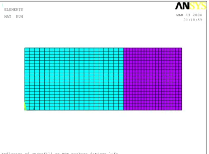
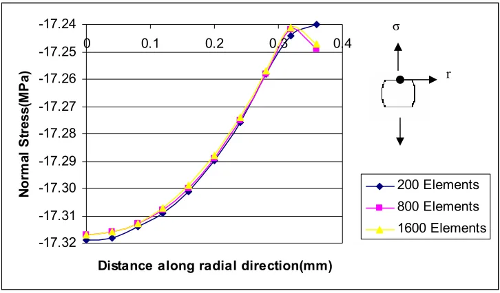
The finite element geometry is meshed using PLANE 182 axisymmetric 4-noded elements as shown in Figure 3.4. There are 800 elements with 861 nodes. Each element has degrees of freedom in both the x-direction and y-direction. The number of elements to be chosen for idealization depends upon the accuracy desired, degrees of freedom, etc. Although the increase in number of elements generally yields an increase in accuracy of the results, there will be certain number of elements beyond which the accuracy cannot be improved by any significant amount. This is termed as convergence of the solution. This convergence is an important factor to be considered in finite element modeling. In this work, convergence of the solution was tested by choosing meshes with 200, 800 and 1600 elements. It was observed that there was no
elements. Figure 3.5 gives an example of the normal stresses obtained for three different meshes. For this case the underfill properties were Eu=3.5GPa, νu=0.3, and αu= 100x10-6/K. The thermal
loading is applied as the temperature is decreased from 25°C to 5°C. The graph depicts the normal stress values along the top boundary of the solder connection. The difference in the values of the normal stresses between 800
1
X
Y
Z
Influence of underfill on BGA package fatigue life
MAR 13 2004 21:18:59 ELEMENTS
MAT NUM
Figure 3.4 Ansys plot showing the mesh of finite element geometry.
elements and 1600 elements was restricted to 0.01 percent. As a result, 800 elements were used in the finite element model.
elements in line 1. In line 2, LESIZE specifies the divisions of unmeshed lines, 1 denotes the line number to be divided, 20 denote the number of element divisions per line. In line 6 the nodes and elements are created within the generated area 1.)
-17.32 -17.31 -17.30 -17.29 -17.28 -17.27 -17.26 -17.25 -17.24
0 0.1 0.2 0.3 0.4
Distance along radial direction(mm)
N
o
rm
al
S
tre
ss
(M
P
a)
200 Elements 800 Elements 1600 Elements
Figure 3.5 Graph depicting the convergence criterion for normal stress values along the top boundary of the solder interconnection. The underfill material properties for this case Eu=3.5GPa, νu=0.3, and αu=100X10-6/K. The
temperature loading is from 25°C to 5°C.
σ
4. Results
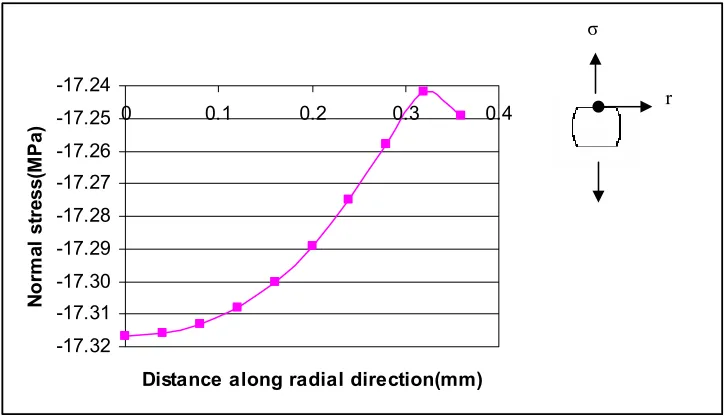
The influence of underfill material properties on the normal stresses in the solder connections was investigated using the finite element model of the unit cell cross section of the BGA package discussed in chapter 3. A thermal loading representative of the temperature range maintained in aerospace applications was applied to obtain the normal cyclic stresses induced at the solder/pad interfaces. In the analysis room temperature is taken to be 25°C. At this
temperature the normal stresses are taken to be zero. Figure 4.1 displays the normal stresses along the top boundary of the radius of the solder connection as the temperature is decreased to 5°C. The underfill properties for this case corresponds to Eu=3.5GPa, νu=0.3, and αu= 100x10 -6/K. Note that the normal stresses across the boundary are similar. For simplicity, in this work
-17.32 -17.31 -17.30 -17.29 -17.28 -17.27 -17.26 -17.25 -17.24
0 0.1 0.2 0.3 0.4
Distance along radial direction(mm)
No
rm
al
s
tr
es
s(
M
P
a)
Figure 4.1 Graph depicting normal stress values along the top boundary
of the solder interconnection. The underfill properties for this case are Eu=3.5GPa, νu=0.3,
and αu= 100x10-6/K. The temperature loading is from 25°C to 5°C. 4.1 Influence of Underfill Parameters
Figure 4.2 displays the magnitude of normal stresses when the temperature is decreased from 25°C to 5°C for Young’s moduli of 2.0GPa, 3.5GPa, 5.0GPa, 6.5GPa, and 8.0GPa. Note in figure 4.2(a) that in some cases the normal stress is in tension and in some cases normal stress is in compression. For example when νu=0.3, the normal stress is in tension for αu=10x10-6/K and is
in compression for αu=40x10-6/K, 70x10-6/K, and 100x10-6/K when the temperature is 5°C.
Figure 4.3 displays how these normal stresses would fluctuate over one temperature cycle (assuming the cycle is sinusoidal).
σ
-30.00 -20.00 -10.00 0.00 10.00
0 20 40 60 80 100
Coefficient of thermal expansion of underfill (1E-6/K) N o rm al S tre ss (M P a) v=0.2 v=0.3 v=0.4
(a)Eu=2.0GPa
-40.00 -30.00 -20.00 -10.00 0.00 10.00
0 20 40 60 80 100
Coefficient of thermal expansion of underfill (1E-6/K) N o rm al S tre ss (M P a) v=0.2 v=0.3 v=0.4
-40.00 -30.00 -20.00 -10.00 0.00 10.00
0 20 40 60 80 100
Coefficient of thermal expansion of underfill (1E-6/K) N o rm al S tre ss (M P a) v=0.2 v=0.3 v=0.4
(c) Eu=5.0GPa
-50.00 -40.00 -30.00 -20.00 -10.00 0.00 10.00
0 20 40 60 80 100
Coefficient of thermal expansion of underfill (1E-6/K) N o rm al S tre ss (M P a) v=0.2 v=0.3 v=0.4
-50.00 -40.00 -30.00 -20.00 -10.00 0.00 10.00
0 20 40 60 80 100
Coefficient of thermal expansion of underfill (1E-6/K)
N
o
rm
al
S
tre
ss
(M
P
a)
v=0.2 v=0.3 v=0.4
(e) Eu=8.0GPa
Figure 4.2 Graphs depicting the normal stresses at the node located at the middle of the top of the solder interconnect.
Figure 4.2(a) displays the magnitude of normal stresses at 5°C for a Young’s modulus of 2.0GPa. As shown in the graph, the normal stresses are becoming greater in absolute magnitude with an increase in the coefficient of thermal expansion of the underfill material. Also, the absolute magnitude of normal stresses increases with increase in Poisson’s ratio of underfill material. For the Young’s modulus of 2.0 GPa, the coefficient of thermal expansion plays a stronger role in influencing the resulting normal stresses than does the Poisson’s ratio.
Figure 4.2(b) depicts the magnitude of normal stresses at 5°C for a Young’s modulus of 3.5 GPa. Similar to what is displayed in Figure 4.2 (a), as the coefficient of thermal expansion and Poisson’s ratio of the underfill material increases, the stresses become greater in absolute magnitude. Again, the coefficient of thermal expansion plays a stronger role in influencing the resulting normal stresses than does the Poisson’s ratio. However, it is evident when comparing the two graphs that as the stiffness of the underfill material increases, νu and αu have more of an
normal stresses range from 2.64MPa to 21.8MPa as αu is increased. When Eu= 3.5 GPa and
νu=0.4, the normal stresses range from 3.11MPa to 32.96MPa. Similarly, when Eu= 2.0 GPa and
αu =100x10-6/ K, the normal stresses range from 5.84MPa to 21.8MPa as νu is increased. When
Eu= 3.5 GPa and αu =100x10-6/ K, the normal stresses range from 10.7MPa to 32.96MPa.
Note from Figures 4.2(c), (d), and (e) that as the stiffness of the underfill material is increased, the coefficient of thermal expansion continues to display an increasing influence on the resulting normal stresses. However as seen when comparing the normal stresses in Figures 4.1(d) and (e), this increase in influence on the normal stresses is becoming minimized. It is also evident when comparing the figures that for a constant αu and νu, an increase in stiffness results
in more compressive normal stresses. In addition, as νu is decreased, the stiffness plays a stronger
role in influencing the magnitude of the normal stresses.
(a) αu=10x10-6/K
5°C 25°C 45°C 25°C
25 °C
(b) αu=40x10-6/K σ
T 5°C
25 °C
25 °C 45 °C 25°C
σ
Figure 4.3 Schematic of the fluctuation of normal stresses over a temperature cycle for the case of Eu=2.0GPa and
νu=0.3 assuming temperature profile is sinusoidal.
Ingeneral, as the temperature is decreased, the absolute magnitude of the stresses are
increasing with an increase in αu, Eu, and νu. Therefore, the most compressive as well as the most
tensile stress for the underfill combination tested is shown in Figure 4.1(e) for the case where
Eu=8.0GPa,νu=0.4, and αu=100x10-6/K.
4.2 Significance of Mode I Cyclic Stresses
It was stated in the introduction that much research has centered around predicting the fatigue life of interconnects based on the Mode II shearing induced upon thermal cycling. It was also stated that research has shown that underfill has been used to provide beneficial residual
(c) αu=70x10-6/K
(d) αu=100x10-6/K
5°C 25°C 45°C 25°C
25 °C σ
T
5°C 25°C 45°C 25°C
25 °C σ
compression in these connections. Larson et al. (2004) developed an equation using nonlinear finite element analysis to predict the steady state stresses caused by contraction of the underfill upon curing using ABAQUS. As mentioned in chapter 2, they tested for various ranges of underfill properties (Eu=0.5 to 8.0GPa, νu=0.2 to 0.4, and %shu = 0.2% to 1.0%) and concluded
that these resulting steady state stresses were in residual compression.
In the present work equation (10) is used to determine if the Mode I cyclic stresses obtained in the previous section are negligible or significant when compared to the residual stresses induced during curing. The Mode I cyclic stresses are added to the steady state stresses according to the schematic 4.4.
Figure 4.4 Schematic showing the addition of Mode I cyclic stresses to steady state stresses.
Appendix B contains a list of the Mode I cyclic stress obtained from the finite element results, the residual steady state stresses obtained from equation (10), as well as the most tensile stress induced from the combination of the constant residual stress and the cyclic stress for every combination of underfill parameters tested. As seen in Appendix B, the resulting cyclic stresses,
σc, are on the same order of magnitude as the residual stresses,σs. The main conclusion from this
work is that these Mode I cyclic stresses are not negligible and need to be considered in the development of a fatigue life model of solder interconnects in BGA packages.
σc+σs
.
σc
+
σs
=
Figure 4.5 displays the plots of the most tensile stresses induced in the solder during one thermal cycle. These stresses correspond to the point highlighted on the schematic in the Figure 4.4. For simplicity, it is assumed in Figure 4.5 that the linear shrinkage upon curing is 0.6% of the underfill material.
-20.00 -10.00 0.00 10.00 20.00 30.00
0 20 40 60 80 100
Coefficient of therm al expansion of underfill(1E-6/K) N o rm al S tr ess( MP a) v=0.2 v=0.3 v=0.4
(a) Eu=2.0GPa
-20.00 -10.00 0.00 10.00 20.00 30.00
0 20 40 60 80 100
Coefficient of thermal expansion of underfill(1E-6/K) No rma l S tre ss (M P a ) v=0.2 v=0.3 v=0.4
-20.00 -10.00 0.00 10.00 20.00 30.00
0 20 40 60 80 100
Coefficient of thermal expansion of underfill(1E-6/K) N o rm al S tr ess( MP a) v=0.2 v=0.3 v=0.4
(c) Eu=5.0GPa
-20.00 -10.00 0.00 10.00 20.00 30.00
0 20 40 60 80 100
Coefficient of thermal expansion of underfill(1E-6/K) No rma l S tre ss (M P a ) v=0.2 v=0.3 v=0.4
-20.00 -10.00 0.00 10.00 20.00 30.00
0 20 40 60 80 100
Coefficient of therm al expansion of underfill(1E-6/K)
N
o
rm
al S
tr
ess(
M
P
a)
v=0.2 v=0.3 v=0.4
(e) Eu=8.0GPa
Figure 4.5 Graphs depicting the most tensile stresses induced in the solder during one thermal cycle when temperature is 5°C and %sh of underfill material is 0.6%.
As depicted in the graph, for a αu = 10x10-6/K, the stresses are becoming more
compressive with stiffer underfill. Also at αu = 40x10-6/K as the underfill becomes stiffer, the
stresses are becoming compressive in nature. For αu = 70x10-6/K and 100x10-6/K the stresses are
becoming more tensile in nature as the stiffness is increased. Also for αu = 10x10-6/K as the
Poisson’s ratio increases the stresses are more compressive in nature. For αu = 40x10-6/K, 70x10 -6/K and 100x10-6/K the stresses are becoming more tensile with an increase in Poisson’s ratio of
the underfill material.
It is interesting to note when observing figure 4.5 the strong dependence on the
coefficient of thermal expansion. Note for all material combinations possessing a coefficient of thermal expansion, αu, greater than around 70x10-6/K, the solder will experience a tensile loading
Referring to Appendix B, for αu = 10x10-6/K as the %sh value increases the stresses are
becoming more compressive. Also for αu = 40x10-6/K as the %sh value increases the stresses
become compressive in nature. Finally, for αu = 70x10-6/K and 100x10-6/K as the %sh value
increases the stresses are less tensile in nature.
-25.00 -20.00 -15.00 -10.00 -5.00 0.00
0.0 2.0 4.0 6.0 8.0
Young's Modulus of Elasticity(GPa)
N
o
rm
al
str
es
s(M
p
a)
%sh=0.2 %sh=0.4 %sh=0.6 %sh=0.8 %sh=1.0
Figure 4.6 Plot depicting the normal stresses for the case whenνu = νs and αu =αs.
While underfill materials in use today have stiffness well below that of solder, typical underfills can possess similar Poisson’s ratio and coefficients of thermal expansion. Assuming the coefficient of thermal expansion and Poisson’s ratio of the underfill are the same as that of the solder material, Figure 4.6 displays the influence of Young’s modulus on the normal stresses in the connections. This plot displays the most tensile stresses obtained during one cycle when adding the cyclic stresses to the steady state stresses obtained from equation (10). The plot demonstrates that as the underfill becomes stiffer the stresses are becoming more compressive in nature. Also, as the linear shrinkage of the underfill material increases the absolute magnitude of normal stresses also increases. It can be deduced from this plot that as long as νu = νs and αu =αs,
The following are several underfill materials which are commonly used in BGA packages: FP4531 with Eu=7.6GPa, νu=0.33, and αu=28x10-6/K; FP4530 with Eu=5.6GPa,
νu=0.33, and αu=43x10-6/K; and 3510 with Eu=2.8GPa, νu=0.33, and αu=70x10-6/K. These
material properties are obtained from technical support at Loctite. The Mode I steady state
stresses obtained using equation (10) are -12.1 MPa, -12.6 MPa and -9.78 MPa respectively. The most tensile stresses obtained from finite element analysis for these cases are 3.25 MPa, 8.13 MPa, and 10.2 MPa, respectively. The most tensile stresses obtained from finite element analysis were added to the steady state stresses obtained from equation (10). The results are depicted in Figure 4.7.
FP 4531
FP 4530
3510
-10.00 -8.00 -6.00 -4.00 -2.00 0.00 2.00
0 20 40 60 80 100
Coefficient of thermal expansion of underfill(1E-6/K)
N
o
rm
al
st
ress(
MP
a)
Figure 4.7 Graph depicting the normal stress values for real underfill material properties.
Figure 4.8 Schematic of sinusoidal plot of Mode I stresses for real underfill material properties.
4.3 Comparison of Mode I Cyclic Stress with Mode II Cyclic Stress
It is evident from section 4.2 that cyclic Mode I stresses should be considered in the development of a fatigue life for BGA interconnects. The development of a fatigue life model based on a fracture approach requires that crack of known size be embedded in the material under investigation and studied.
The following example provides a guideline for how researchers can determine the approximate loading (both Mode I and Mode II) to apply experimentally to the test specimen in the development of an appropriate fracture based fatigue life model. Consider a one inch by one inch BGA package for aerospace applications where the temperature is cycled from 5°C to 45°C. For simplicity a ten by ten array of solder interconnects is depicted in the Figure 4.9. The
T°C
-20 5
-5
-10
-15
3510 FP4530
FP4531
Normal stress
-9.78MPa
-12.6MPa -12.1MPa 0.41MPa
-4.45MPa
-8.83MPa
-20.0MPa
difference in coefficient of thermal expansion of chip carrier and PCB is taken as 1.6x10⁻⁶/K. The stand off height of each joint is taken as 0.5mm and radius of the pad is 0.4mm. The solder interconnects in this BGA package are made of eutectic solder with Es=32GPa and Poisson’s
ratio, υs=0.3 and are subjected to a thermal loading from 25°C to 5°C. According to equation (5),
the Mode II shear stress, τ in the solder interconnects at a distance of L=18mm is 14.17MPa and at a distance of L=6mm is 4.72MPa.
1: L=18mm τ = 14.17MPa 2: L=6mm τ = 4.72MPa
Figure 4.9 Schematic of top view of a ten by ten array of solder interconnects in BGA package (the numbered joints represents the joints for which shear stress is calculated).
Assume, for example, that the 3510 underfill is being considered and the fatigue life of the joint located at 6 mm from the center of the package is in question. During one thermal cycle, the shear stress arising from the mismatch in coefficient of thermal expansion between chip
5. Conclusions and Recommendations
The influence of underfill on BGA package fatigue life has been investigated in this present research. With an increase in effort to reduce the size of electronic packages, much of the research has been motivated towards the reliability of solder joints in present day technology. A finite element model of unit cell geometry of a BGA package was developed using ANSYS 7.1 to analyze the significance of Mode I cyclic loading in the solder interconnects. It was proven that these Mode I cyclic stresses are significant and are of same order of magnitude when compared to Mode I steady state stresses obtained by Larson and Verges (2004).
Also the influence of underfill parameters such as Eu, υu, and αu on Mode I cyclic stresses
have been determined. It has been observed that as the coefficient of thermal expansion of
underfill material increases, the amplitude of the normal cyclic stresses increases. For an increase in Poisson’s ratio and stiffness of underfill material, the amplitude of the Mode I cyclic stresses also increases. However, it is evident that as the stiffness of the underfill material increases, νu
and αu have a greater influence on the resulting normal stresses.
When adding the residual stresses induced in the solder upon curing of the underfill to the cyclic Mode I stresses caused by mismatch of solder and underfill properties during thermal cycling, a strong dependence on the coefficient of thermal expansion is observed. For a linear shrinkage of 0.6% of the underfill material, results indicate for all material combinations
possessing a coefficient of thermal expansion, αu, greater than around 70x10-6/K, the solder will
in Eu, νu, and αu, and a decrease in %sh. Three popular underfills were also investigated in this
study: FP4531, FP4530, and 3510. In comparing these three underfills, it is observed that during any one thermal cycle, use of the 3510 underfill would cause the solder to experience tension during a portion of the thermal cycling.
This work proves that more research is to be geared towards experimentally determining the fatigue life of fractured joints subjected to a combined Mode I and Mode II cyclic loading. It follows that such results would aide in the development of a fatigue life equation that
References
1. Larson, M.C., Liu, X., and Verges, M. A., 2004, “Predicting Residual Stresses in Area Array Packages Induced by Underfill Shrinkage”, submitted to the Journal of
Microelectronics Reliability.
2. Larson, M. C. and Verges, M. A., 2003, “Extending the Fatigue Life of Solder Grid Array (SGA) Electronic Packages”, Journal of Electronic Packaging, Vol.125, pp.18-23. 3. Ligi, Z., Li, W., Xiaoming, X., and Kempe, W., 2002, “An Investigation on Thermal
Reliability of underfilled PBGA Solder Joints”, IEEE Transactions on Electronics Packaging Manufacturing, vol-25, No.4, pp. 284-288.
4. Pyland, J., Pucha, R., and Sitaraman, S., 2001, “Effect of Underfill on BGA reliability”,
Electronic Components and Technology Conference, pp. 85-90.
5. Nemeth, N., Illetalvi-Vitez, Z., and Harsanyi, G., 2000, “Review of Reliability of Advanced Component Packaging Technologies”, 2000 Proceedings: 50th Electronic Components Technology Wednesday poster session, pp.1605-1609.
6. Wang, L., and Wong, C.P., 2000, “Recent advances in the underfill technology for Flipchip, Ball Grid Array and Chip Scale Package Applications”, International
symposium on electronic materials and packaging:Nov 30-Dec 2, Hong Kong, pp.224-231.
7. T.Burnette, Z.Johnson, T.Koschmieder, and W.Oyler, 2000, “underfilled BGA’S for ceramic bga packages and board level reliability”, 2000 Proceedings: 50th Electronic Components & Technology Conference, May 21-24, Las Vegas, Nevada, USA, pp.1221-1226.
8. S.C.Hung, P.J.Zheng, S.C.Lee, S.H.Ho, and H.N.Chen, 2000, “Thermal Cyclic Fatigue of Interconnect of a Flex type BGA”, Electronic Components and Technology Conference, pp.1384-1391.
9. Kaga, Y., Yu, Q., Shiratori, M., 1999, “Thermal Fatigue Assessment for Solder Joints of Underfill Assembly”, Advances in Electronic Packaging, Vol.26, pp.271-275.
10. C. Basaran, and R. Chandraroy, 1997 “Finite element simulation of the temperature cycling tests”, IEEE Transaction component hybrids and Manufacturing Technology , Vol.20 , pp.530-536.
11. Verges, M. A., 1999, “An Investigation of Interconnect Geometry and Fatigue Life of Ball Grid Array Electronic Packages”, Ph.D.thesis.
12. Bjorndahl, W.D., Selk, K., and Chen, W., 1997, “Surface Mount Technology Capabilities and Requirements”, IEEE Aerospace Conference Proceedings ,Vol.4, pp.285-291.
13. Yao, D., Z. Zhang, and J.K.Shang, 1996, “An Experimental Technique for Studying Mixed-Mode Fatigue Crack Growth in Solder Joints”, Journal of Electronic Packaging, Vol.118, pp. 45-48.
14. H.D.Solmon, E.D.Tolksdorf, 1995, “Energy Approach to the Fatigue of 60/40 Solder: Part I-Influence of Temperature and Cycle Frequency”, Journal of Electronic Packaging
, Vol.117, pp.130-135.
15. Pao, Y., 1992, “A Fracture Mechanics approach to thermal fatigue life prediction of joints”, IEEE transactions on components, hybrids, and manufacturing, Vol.15, pp.559-570.
16. Vaynman, S., McKeown, S. A., 1991, “Energy based Methodology for the Fatigue–life prediction of Solder materials”, Electronic components and Technology Conference, pp.671-676.
17. Frear, D., Morgan, H., Burchett, S., and Lau, J., 1994, The Mechanics of Solder Alloy Interconnects, Van Nostrand Reinhold Publications, New York.
18. Anderson T.L., IInd Edition, 1995, Fracture Mechanics Fundamentals and Applications, CRC Press, Boca Raton.
19. Lau, J., 1995, Ball Grid Array Technology, Mc-Graw Hill Publications, New York. 20. Hwang, Jennie, S., 1995, Ball Grid Array & Fine Pitch Peripheral Interconnections A
Appendix A
FINISH /CLEAR
/TITLE, Influence of underfill on BGA package fatigue life /PREP7
ET, 1, PLANE182,,, 1 !element type plane182 with axisymmetric elements DOF, UX, UY
! Section 3.3
MP, EX, 1,32E9 ! Young’s modulus of solder material MP, PRXY, 1, 0.3 ! Poison’s ratio
MP, ALPX, 1, 24.1E-6 ! Coefficient of thermal expansion
MP, EX, 2, 5.0E9 ! Young's modulus of underfill material MP, PRXY, 2, 0.2 ! Poison’s ratio
MP, ALPX, 2, 10E-6 ! Coefficient of thermal expansion TB, BISO, 1
TBDATA, 1,33E6 ! Yield stress (Pa) TBDATA, 2, 0.01 ! Tangent modulus (Pa)
! Section 3.1
!creation of key points to generate the two rectangles K, 1, 0, 0
A, 1, 2, 3, 4 A, 2, 3, 6, 5
AGLUE, ALL ! To glue both the rectangles
! Section 3.5
! MESHING MAT, 1
LESIZE, 1,,, 20 LESIZE, 2,,, 20 LESIZE, 3,,, 20 LESIZE, 4,,, 20 AMESH, 1 Mat, 2
LESIZE, 7,,, 20 LESIZE, 6,,, 20 LESIZE, 5,,, 20 AMESH, 2
! Section 3.2
! Constraint equations to implement the condition for top edge ! of the rectangle to move in uniform y-direction
CE, 1, 0, 42, UY, 1, 61, UY, -1, J=2
*DO, I, 61, 44, -1
CE, J, 0, I, UY, 1, I-1, UY, -1, J=J+1
*ENDDO
CE, 20, 0, 43, UY, 1, 22, UY, -1, CE, 21, 0, 22, UY, 1, 443, UY, -1, J=22
*DO, I, 443, 460, 1
CE, J, 0, I, UY, 1, I+1, UY, -1, J=J+1
*ENDDO
CE, 40, 0, 461, UY, 1, 442, UY, -1, ! Boundary conditions
NSEL, S, LOC, Y, 0 D,ALL,UX
D, ALL, UY
D, ALL, UX
NSEL, S, LOC, Y, 0.00025 D, ALL, UX
NSEL, S, LOC, X, 0.000635 D, ALL, UX
TREF, 298 !reference temperature ALLSEL
SAVE FINI
! Section 3.4
/SOLUTION
SOLCONTROL, ON ! Specifies whether to use optimized nonlinear
!solution defaults and some enhanced internal !solution algorithms.
TIME, 1.0E-8
DELT, 1.0E-8, 1.0E-9, 1.0E-8 !specifies time step size to be used for load step OUTRES, ALL, 100000 !controls the solution data written to the database OUTPR, ALL, 100000 !controls the solution output
TUNIF, 298 !uniform temperature SOLVE
SAVE
DELT, 1.0E-6, 1.0E-6, 500000.0 OUTRES, ALL, ALL
OUTPR, ALL, LAST
BF, ALL, TEMP, 278 !uniform temperature reduction SOLVE
SAVE FINISH
! To display the solution /POST1
PLNSOL, S, Y FINISH
Table B.1 The most tensile stresses induced in the solder during one thermal cycle when temperature is 5°C and Eu = 2.0GPa
(a)ν
u= 0.2
(b)ν
u= 0.3
(c)ν
u= 0.4
% sh
αu
(1E-6/K) σs (Pa) σc (Pa) σs + σc (Pa)
% sh
αu
(1E-6/K) σs (Pa) σc (Pa) σs + σc (Pa)
% sh
αu
(1E-6/K) σs (Pa) σc (Pa) σs + σc (Pa)
0.2 10 -1.34E+06 3.17E+06 1.83E+06 0.2 10 -1.53E+06 2.97E+06 1.45E+06 0.2 10 -1.78E+06 2.64E+06 8.54E+05
0.2 40 -1.34E+06 1.60E+05 -1.18E+06 0.2 40 -1.53E+06 1.40E+06 -1.22E+05 0.2 40 -1.78E+06 5.37E+06 3.59E+06
0.2 70 -1.34E+06 2.84E+06 1.51E+06 0.2 70 -1.53E+06 5.78E+06 4.25E+06 0.2 70 -1.78E+06 1.34E+07 1.16E+07
0.2 100 -1.34E+06 5.84E+06 4.51E+06 0.2 100 -1.53E+06 1.01E+07 8.62E+06 0.2 100 -1.78E+06 2.18E+07 2.00E+07
0.4 10 -2.67E+06 3.17E+06 4.98E+05 0.4 10 -3.05E+06 2.97E+06 -7.86E+04 0.4 10 -3.56E+06 2.64E+06 -9.27E+05
0.4 40 -2.67E+06 1.60E+05 -2.51E+06 0.4 40 -3.05E+06 1.40E+06 -1.65E+06 0.4 40 -3.56E+06 5.37E+06 1.81E+06
0.4 70 -2.67E+06 2.84E+06 1.71E+05 0.4 70 -3.05E+06 5.78E+06 2.72E+06 0.4 70 -3.56E+06 1.34E+07 9.81E+06
0.4 100 -2.67E+06 5.84E+06 3.17E+06 0.4 100 -3.05E+06 1.01E+07 7.09E+06 0.4 100 -3.56E+06 2.18E+07 1.83E+07
0.6 10 -4.01E+06 3.17E+06 -8.38E+05 0.6 10 -4.58E+06 2.97E+06 -1.61E+06 0.6 10 -5.34E+06 2.64E+06 -2.71E+06
0.6 40 -4.01E+06 1.60E+05 -3.85E+06 0.6 40 -4.58E+06 1.40E+06 -3.18E+06 0.6 40 -5.34E+06 5.37E+06 2.48E+04
0.6 70 -4.01E+06 2.84E+06 -1.16E+06 0.6 70 -4.58E+06 5.78E+06 1.20E+06 0.6 70 -5.34E+06 1.34E+07 8.03E+06
0.6 100 -4.01E+06 5.84E+06 1.84E+06 0.6 100 -4.58E+06 1.01E+07 5.57E+06 0.6 100 -5.34E+06 2.18E+07 1.65E+07
0.8 10 -5.34E+06 3.17E+06 -2.17E+06 0.8 10 -6.11E+06 2.97E+06 -3.13E+06 0.8 10 -7.12E+06 2.64E+06 -4.49E+06
0.8 40 -5.34E+06 1.60E+05 -5.18E+06 0.8 40 -6.11E+06 1.40E+06 -4.70E+06 0.8 40 -7.12E+06 5.37E+06 -1.76E+06
0.8 70 -5.34E+06 2.84E+06 -2.50E+06 0.8 70 -6.11E+06 5.78E+06 -3.31E+05 0.8 70 -7.12E+06 1.34E+07 6.25E+06
0.8 100 -5.34E+06 5.84E+06 5.00E+05 0.8 100 -6.11E+06 1.01E+07 4.04E+06 0.8 100 -7.12E+06 2.18E+07 1.47E+07
1.0 10 -6.68E+06 3.17E+06 -3.51E+06 1.0 10 -7.63E+06 2.97E+06 -4.66E+06 1.0 10 -8.91E+06 2.64E+06 -6.27E+06
1.0 40 -6.68E+06 1.60E+05 -6.52E+06 1.0 40 -7.63E+06 1.40E+06 -6.23E+06 1.0 40 -8.91E+06 5.37E+06 -3.54E+06
1.0 70 -6.68E+06 2.84E+06 -3.84E+06 1.0 70 -7.63E+06 5.78E+06 -1.86E+06 1.0 70 -8.91E+06 1.34E+07 4.46E+06
Table B.2 The most tensile stresses induced in the solder during one thermal cycle when temperature is 5°C and Eu = 3.5 GPa
(a) ν
u= 0.2
(b) ν
u= 0.3
(c) ν
u= 0.4
%
sh
αu
(1E-6/K) σs (Pa) σc (Pa) σs + σc (Pa) % sh
αu
(1E-6/K) σs (Pa) σc (Pa) σs + σc (Pa)
% sh
αu
(1E-6/K) σs (Pa) σc (Pa)
σs + σc (Pa)
0.2 10 -2.22E+06 3.93E+06 1.71E+06 0.2 10 -2.54E+06 3.61E+06 1.08E+06 0.2 10 -2.96E+06 3.11E+06 1.44E+05
0.2 40 -2.22E+06 9.52E+05 -1.27E+06 0.2 40 -2.54E+06 3.37E+06 8.28E+05 0.2 40 -2.96E+06 9.06E+06 6.10E+06
0.2 70 -2.22E+06 5.82E+06 3.60E+06 0.2 70 -2.54E+06 1.03E+07 7.80E+06 0.2 70 -2.96E+06 2.14E+07 1.84E+07
0.2 100 -2.22E+06 1.07E+07 8.48E+06 0.2 100 -2.54E+06 1.73E+07 1.48E+07 0.2 100 -2.96E+06 3.30E+07 3.00E+07
0.4 10 -4.44E+06 3.93E+06 -5.15E+05 0.4 10 -5.08E+06 3.61E+06 -1.46E+06 0.4 10 -5.92E+06 3.11E+06 -2.82E+06
0.4 40 -4.44E+06 9.52E+05 -3.49E+06 0.4 40 -5.08E+06 3.37E+06 -1.71E+06 0.4 40 -5.92E+06 9.06E+06 3.14E+06
0.4 70 -4.44E+06 5.82E+06 1.38E+06 0.4 70 -5.08E+06 1.03E+07 5.27E+06 0.4 70 -5.92E+06 2.14E+07 1.55E+07
0.4 100 -4.44E+06 1.07E+07 6.26E+06 0.4 100 -5.08E+06 1.73E+07 1.22E+07 0.4 100 -5.92E+06 3.30E+07 2.70E+07
0.6 10 -6.66E+06 3.93E+06 -2.74E+06 0.6 10 -7.61E+06 3.61E+06 -4.00E+06 0.6 10 -8.88E+06 3.11E+06 -5.78E+06
0.6 40 -6.66E+06 9.52E+05 -5.71E+06 0.6 40 -7.61E+06 3.37E+06 -4.25E+06 0.6 40 -8.88E+06 9.06E+06 1.80E+05
0.6 70 -6.66E+06 5.82E+06 -8.38E+05 0.6 70 -7.61E+06 1.03E+07 2.73E+06 0.6 70 -8.88E+06 2.14E+07 1.25E+07
0.6 100 -6.66E+06 1.07E+07 4.03E+06 0.6 100 -7.61E+06 1.73E+07 9.70E+06 0.6 100 -8.88E+06 3.30E+07 2.41E+07
0.8 10 -8.88E+06 3.93E+06 -4.96E+06 0.8 10 -1.02E+07 3.61E+06 -6.54E+06 0.8 10 -1.18E+07 3.11E+06 -8.74E+06
0.8 40 -8.88E+06 9.52E+05 -7.93E+06 0.8 40 -1.02E+07 3.37E+06 -6.79E+06 0.8 40 -1.18E+07 9.06E+06 -2.78E+06
0.8 70 -8.88E+06 5.82E+06 -3.06E+06 0.8 70 -1.02E+07 1.03E+07 1.89E+05 0.8 70 -1.18E+07 2.14E+07 9.55E+06
0.8 100 -8.88E+06 1.07E+07 1.81E+06 0.8 100 -1.02E+07 1.73E+07 7.16E+06 0.8 100 -1.18E+07 3.30E+07 2.11E+07
1.0 10 -1.11E+07 3.93E+06 -7.18E+06 1.0 10 -1.27E+07 3.61E+06 -9.08E+06 1.0 10 -1.48E+07 3.11E+06 -1.17E+07
1.0 40 -1.11E+07 9.52E+05 -1.02E+07 1.0 40 -1.27E+07 3.37E+06 -9.33E+06 1.0 40 -1.48E+07 9.06E+06 -5.74E+06
1.0 70 -1.11E+07 5.82E+06 -5.28E+06 1.0 70 -1.27E+07 1.03E+07 -2.35E+06 1.0 70 -1.48E+07 2.14E+07 6.59E+06