Power Efficient Carry Skip Adder Based on
Static 125nm CMOS Technology
R. Abinaya S. Gayathri
BE Student BE Student
Department of Electronics & Communication Engineering Department of Electronics & Communication Engineering SNS College of Technology, Coimbatore - 35 SNS College of Technology, Coimbatore - 35
S. Atchaya G. Hemanth Kumar
BE Student BE Student
Department of Electronics & Communication Engineering Department of Electronics & Communication Engineering SNS College of Technology, Coimbatore - 35 SNS College of Technology, Coimbatore - 35
G. Naveen Balaji
Assistant Professor
Department of Electronics & Communication Engineering SNS College of Technology, Coimbatore - 35
Abstract
In a digital circuit theory, combinational logic is a type of digital logic implemented by Boolean circuits, where the output is pure function of the present input. A carry skip adder which is also known as carry by pass adder is an adder implementation that improves on the delay of a ripple carry adder with little effort compared to other adders, In which, it have the low power consumption, a high degree of regularity and simplicity that the carry ripple chain is connected to n-input AND gate. The resulting bit is used as the select bit a multiplexer that switches either the last carry bit or the carry-in to the carry-out signal. The behaviour of the efficient Carry Skip Adder is designed using tanner eda tools which was useful and the currently existing carry skip adder is designed using xilnx software and lastly the layout for this research is designed with the help of multisim. With help of this research many newly created circuits can designed much smaller.
Keywords: Carry Skip Adder, CMOS, Static CMOS, 125nm, Tanner, Multisim, Xilinx, Half Adder, Full Adder, Ripple Carry Adder
_______________________________________________________________________________________________________
I. INTRODUCTION
Adders play a major role in combinational circuits. A combinational circuit is said to be a circuit in which the output is depend upon the function given by the input which is implemented by various Boolean expression according to the connection given to each gate, though this may be considered controversial such as half adder, full adder, half subtractor, full subtractor, multiplexer, demultiplexer, encoder and decoder are also shared its classification under combinational logic. Carry skip adder consists of a simple ripple carry adder with speed up chain called skip chain the chain defines the distribution of ripple carry blocks if the carry is propagated at all position in the block then the carry signal entering into the block can directly bypass the carry skip adder optimization problem for variable block size and multiple levels for an arbitrary device process node was solved. A carry skip adders is also considered to be carry bypass adder, it is an adder implementation that improves on the delay of a ripple carry adder with little effort compared to other adders. This research paper is for designing a carry skip adder in 125nm static technology.
II. EXISTING SYSTEM
A full adder proceeds two binary numbers plus a carry or overflow bit. The output is a sum and carry bit. Full adders are generally linked to each other to append bits to an arbitrary length of bits such as 32 or 64 bit. A full adder is competently two half adders an ‘XOR’ and an ‘AND’ gate connected by an ‘OR’ gate. Half adder is a digital circuit that executes summation of numbers. The half adders adds two binary digits called as augend and addend and bring forth two outputs as sum and carry , ‘XOR’ is appertained to both input to produce sum and ‘AND’ gate is appertained to both inputs to produce carry . A Half Adder is made up of multiple gates which performs very basic operations according to the connections made in the CMOS (Complementary Metal Oxide Semiconductor
exclusive or, that is, a ‘1’ output results if one, and only one, of the inputs to the gate is ‘1’. If both inputs are ‘0’ or both are ‘1’, a ‘0’ output results. In ‘and’ gate ,only multiplication operation can be done if the both input are same the output will be the same as the input and if the inputs are different then the output will ‘0’. In ‘not’ gate, contains only one input and the output is the output of the input if the input is ‘1’ then the output will be ‘0’ vice versa.
Fig. 1.1: Block diagram of Half Adder:
In fig 1.1 we can analyze that a half Adder consist of two inputs ‘a’ and ‘b’ and output ‘sum’and ‘carry’. Carry Skip Adder is buildup of multiple full adders and full adders are made with two half adder A truth table is a logically based mathematical table that expatiates the conceivable sequels of scenario the truth table suppresses the truth values thar would appear under the premises of the given scenario. The rows of a basic truth table contain the Boolean logic true or false values while the columns list the premises of a scenario as well as conclusion.
Fig. 1.2: Logic diagram of Half Adder:
In fig 1.2 Gates like ‘xor’, ‘not’, and ‘and’ Gates which are used to process the inputs and give the output. Each gate has a difference type of process algorithm based the connection given to the CMOS. The Boolean expression of the half Adder is as follows
SUM = ab’ + ba’ CARRY= a . b
Fig. 1.3: Truth Table of Half Adder:
In Fig 1.3 is a truth table of the half Adder which portrays the output of that logical circuit. A half Adder is a basic arithmetic processor which perform only subtraction its only function is to deduce a single bit binary from the input
III. CARRY SKIP ADDER
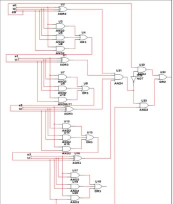
Fig. 2.1: Block diagram of Carry Skip Adder
In Fig2.1 we can analyze that a Carry Skip Adder consist of two inputs ‘a0’, ‘b0’, ‘c0’, ‘a1’, ‘b1’, ‘a2’, ‘b2’, ‘a3’ and ‘b3 whereas output ‘sum’and ‘carry’
In Fig 2.2 When the inputs are given through the respective labels gates present the circuits will process the data and perform the arithmetic operation subtraction and produce the Respective output sum and carry
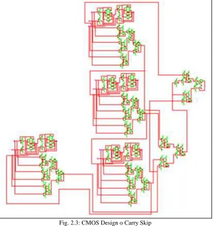
Fig. 2.3: CMOS Design o Carry Skip
In Fig 2.3The above Carry Skip Adder is designed using static cmos algorithm under 125 nm which is quite efficient and the results are same as the currently existing one When the inputs are given through the respective labels gates present the circuits will process the data and perform the arithmetic operation subtraction and produce the Respective output sum and carry
IV. RESULTS
Output
Waveform of CMOS design of Carry Skip Adder:
V. CONCLUSION
It has been observed from the simulation results that performance of adder architectures varies with various CMOS design. The output of these two designs of Carry Skip Adder are same. The current fabrication size of Carry Skip adder is 125nm.If the fabrication size reduced to less than 100nm, the adder performance varies and can be absorbed using static (CMOS) technology. From this research the (CMOS) can be achieved by operating point within 0.9v.This research is very useful and more advantageous in future microprocessor industries.
REFERENCES
[1] N.Weste and K.Eshraghian,--Principles of VLSI Design, A system perspective, Reading, MA:Addison-Wesley,1993.
[2] Shital Baghel, Pranay Kumar Rahi,Nishant Yadav,2015,”(CMOS) Half Adder Design & Simulation Using Different Foundry”, International al Journal
of Innovative Science, Engineering & Technology(IJISET),Vol.2 Issue 3,pp.195-622,Aug.2000.
[3] Ming-Bo Lin, “Introduction to VLSI systems A logic, circuit and system perspective,” Taylor & Fransis group,ch. 7
[4] Neil H.E.Weste,DavidHarris and Ayan Banaerjee,”CMOS VLSI Design”.Pearson Education,Inc.,pp.11,Third edition,2005.
[5] M. Morris Mano, Michael D. Cilleti “Digital Design”,4th edition,pp.143,2012..
[6] Kaushik Roy and S.C.Prasad,” Low power CMOS VLSI circuit design”,Willey,pp.1-129,2000
[7] E.M.M.Poncino,(1996)Power Consumption of Static and Dynamic CMOS circuits, IEEE,2nd International Conference on ASIC,pp.425-427.
[8] P.S.Aswale and S.S.Chopade,(2013) Comparative Study of Different Low Power Design Techniques for reduction of Leakage power in CMOS VLSI
Circuits,IJCA(0975-8887,Volume 70-NO.1
[9] R.L.Geiger, P.E.Allen, N.R.Strander(2013) VLSI Design techniques for Analog and Digital Circuits, McGraw Hill,New Delhi, India,.[page.No.597-ch7
[10] S. Shobana, R. Ramya, K.K. Rashika, G. Naveen Balaji, K. Boopathiraja, “Hamming Window Function based FFT Analysis of Advanced Approximate
Adder design in 125nm CMOS technology using Transmission gates”, International Journal of Science and Innovative Engineering & Technology, Vol. 5, Issue: May 2018.
[11] G.NaveenBalaji,P.Malini,T.Poovika, P.Shanmugavadivu, “14T Full Adder in 125nm CMOS technology for FFT applications using piecewise constant