Universal Asynchronous Receiver and Transmitter
Implementation on 40nm Technology
#Satyendra Kumar and Ankit Singh*
#Head of Department, *Student
Department of Electronics and Communication Engineering, Jaypee Institute of Information Technology Noida, India.
Date of publication (dd/mm/yyyy): 10/03/2018
Abstract – This paper presents the design of Universal Asynchronous Receiver and Transmitter module using various tools available in Cadence Design Systems and Xilinx namely: Cadence RC compiler, Cadence Encounter and Xilinx Design Suite 14.1i . Test bench simulation has been performed using the Xilinx Design in combination with Model Sim6.5e, while worst path analysis, power and timing analysis have been performed in Cadence RC Compiler. A UART module mainly consists of three components, a Transmitter, a Receiver, and a BAUD Rate Generator. A BAUD Rate Generator generates the clock for the Receiver and Transmitter. A BAUD rate is the symbol rate i.e. data rate thus higher the rate higher is the speed. For this simulation and analysis, we have use a baud rate of 9600 and the technology used is 40nm. For FPGA implementation a clock frequency of 25MHz has been used, and for slack timing and worst path analysis time periods ranging from 1000000ps to 1000ps, thus giving a frequency range of 100MHZ to 1GHz. NC Simulator is used for pre-simulation and post simulation which is done using the generated Netlist from Cadence and the 40nm Front End library from Cadence. For frequency analysis Cadence RC Compiler is used to generate schematic on a 40nm technology. Cadence SoC Encounter is used for the layout for optimization and routing.
Keywords – UART, Baud Rate, Frequency Analysis, Transmitter, Receiver.
I. I
NTRODUCTIONUART stands for Universal Asynchronous Receiver Transmitter. A UART module is an integrated circuit that consists of mainly three components, a Transmitter, a receiver and a baud rate generator. A UART chip is an electronic circuit that transmits and receives data through the serial port. A transmitter is in basic a shift register to which data is loaded parallel and then data is shifted out serially through the MSB or LSB. Thus, it converts bytes into serial bits for transmission, and vice versa. It also generates and removes extra bits like the start and stop bits that are appended to each symbol/character for communication configuration, these bits are called parity bits. The receiver on the other hand shifts the data in a register bit-by-bit thus reassembling the original data in another register with parity bits removed. A baud rate generator is used to generate a transmitter/ receiver specific clock and provide a specific baud rate for data transmission, similarly on the receiver UART baud rate generator is used to generate another clock for receiving and reassembly of the original data.
Since UART works in the asynchronous mode of data transmission both the transmission and the receiver ends need their own clocks separate from the system chocks to form an understanding in communication i.e. both the transmitter and receiver must agree on some sort of timing parameters in advance and special bits are added to each symbol which are used to synchronize both the units.
Whenever a symbol is given to the UART module for transmission a „Logic LOW‟ is sent representing the „START BIT‟. This „START BIT‟ tells the receiver that data transmission is about to begin which in turn forces the receiver clock to be in synchronisation with the transmitter. After the Start Bit, the individual bits of the word of data are sent, with the Least Significant Bit (LSB) being sent first. Each bit in the transmission is transmitted for exactly the same amount of time as all of the other bits, and the receiver “looks” at the wire at approximately halfway through the period assigned to each bit to determine if the bit is a 1 or a 0. Then at last one Stop Bit is sent by the transmitter. Because asynchronous data is “self-synchronous”, if there is no data to transmit, the transmission line can be idle. In this simulation analysis values are read half way through the period i.e. at the middle of the level. For example, if it takes four seconds to send each bit, the receiver will examine the signal to determine if it is a 1 or 0 after two seconds have passed because by this method chances of error in bit detection will be less as there will be less chance later in bit change from 1 to 0 or from 0 to 1, then it will wait for four seconds and then examine the next incoming bit. Thus, making the asynchronous data “self-synchronous”.
II. I
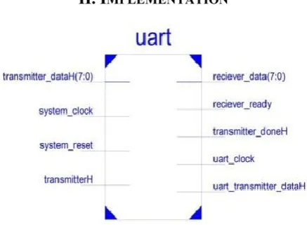
MPLEMENTATIONFig. 2. Block Diagram
Pin Description
system_clock The system clock supplied to the UART IC
system_reset Reset(Active LOW) transmitter_data(7:0) Parallel data input lines. transmitterH Transmitter ready receiver_ready Receiver Ready
uart_clock BUAD rate generated clock uart_transmitter_dataH UART Transmitter Pin
receiver_data(7:0) UART output data lines transmitter_doneH UART transmission status
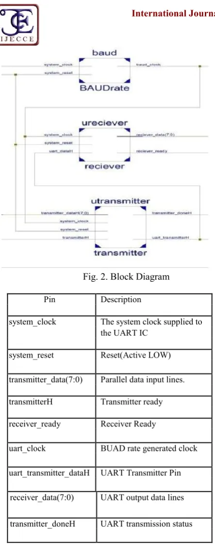
BAUD Generator:
Baud is a measurement of transmission speed. Baud Rate represents the number of bits that are actually being sent over the media, the Baud count includes the overhead bits Start, Stop and Parity that are generated by the sending UART and removed by the receiving UART. By the use of synchronisation and training bits in the transmission signal the two baud rate generators each at the transmitter and receiver generate the same clock.
Transmitter:
The above figure shows the block diagram for the UART Chip. As it can be seen in above there are two main pins for data transmitter_dataH (For Transmission) and receiver_data (For receiver operation). The parallel data input and output pins sets are marked as the
transmitter_dataH (7:0) and the receiver_data (7:0) respectively for inputting data for transmission and taking out the recovered data.
The basic data frame for a UART Transmission can be described as:
Start Bit ‘0’ 8 bit Data Stop Bit ‘1’
Initially a „1 to 0‟ or a „High to Low‟ transition is sent to let the receiver know that the transmission will begin shortly and the parity bits are sent to synchronize the receiver baud clock. In this case for simulation we have taken start bit as „LOW‟ and the stop bit as ‟HIGH‟. Thus, if the data to be sent is: 10110101 then the corresponding data frame sent will be as 0101101011. Thus at a time at least “ten” bits are sent for sending one byte of data. Using this approach increases the bits sent thus reducing the usable data rate. Thus, if data is to be transmitted and the transmitterH register is empty the data is immediately sent. Thus, a transmitter in simple terms performs parallel to serial conversion of the data. Using a shift register data is be shifted either right or left and bit by bit and sent. The either of the bits from the terminal in the register is sent. The whole process of shifting and transmitting is repeated till the time the last bit is sent. When all the bits are sent a „1‟ is sent to notify that the data has been sent and the transmission has ended.
Receiver:
III. F
INITES
TATEM
ACHINEFig. 3. Transmitter FSM
The above figures show the Receiver and the Transmitter Finite State Machines (FSMs). And describe the internal working of transmitter and the receiver modules of UART. The transmitter has five states: Idle, Start, Wait, Shift and Stop.
Idle for ready/free state. Start corresponding to initiation. Wait for delay and storing MSB and transmitting. Shift for rotating the data in the temporary register. Finally the Stop State is used to represent completion of transmission.
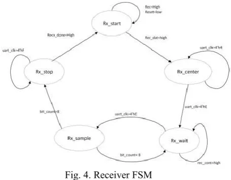
Fig. 4. Receiver FSM
Similarly, the receiver module also works in five states: Start: Here the receiver waits for a „LOW‟ until it receives it stays in this state.
Centre: once a LOW bit is received the receiver shift into this state and waits for the centre of the pulse and then goes to the next state.
Wait: once the first bit is transmitted receiver stores it in a shift register and proceeds to Sample state and once again records another bit at the centre. This process is repeated seven times.
Stop: once all eight bits are received and a HIGH is received, receiver shifts to this state and stays until data is reassembled and sent (i.e. for 16 clock cycles). Once this is done receiver_done is set high and the module returns to Start State.
IV. M
ODELS
IM ANDX
ILINXS
IMULATIONFig. 5. Waveform Generated on Model Sim
As in above generated waveforms from Model Sim initially receiver_data[7:0] register is empty and starts to be filled and rotated with bits till finally 8 bits are received and stored. Data for transmission is loaded on to the transmitter_dataH[7:0] register.
Baud Rate Generator:
In general acts as a frequency divider since the modules may not work at same clock supplied by the system. The division factor can be mathematically obtained by using the system clock frequency and the required baud rate. In this case the baud rate required is 9600bps and the system clock frequency is 25MHz thus the division factor is:
25 ∗ 106
Divide Factor = 16∗9600 = 162.7
Thus, the division factor is 163. This factor can be increased or decreased in order to decrease or increase the baud/ data rate thus allowing to control the rate of transmission. The same has been done using Cadence Simulator and same resulting waveforms have been generated thus showing uniformity in this simulation.
The Pre-Simulation results when used without any technology
Fig 6. Pre-Simulation
Fig. 7. Post-Simulation
V. C
ADENCEE
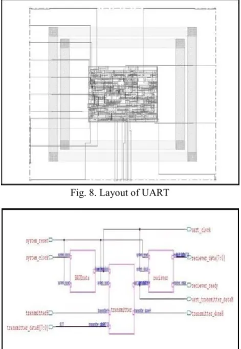
NCOUNTERWe have used 40nm Technology. This layout also shows advanced information like topology and rings. As seen above using the cadence SOC Encounter, a layout schematic has been generated for the IC Chip.
Fig. 8. Layout of UART
Fig. 9. Schematic Generated On Cadence RTL Compiler
VI. A
NALYSIS ANDR
ESULTSCadence Encounter uses the generated Netlist by RTL compiler. Encounter performs optimization and considers Timing, power and area and performs top-down global RTL design Synthesis to accelerate silicon realization. Using Cadence RTL Encounter tool various slack times, Cell Area and Power levels have been acquired and further plotted in the following graph:
Table 1. Frequency Analysis.
Frequencies Slack Cell Net
time(ps) Area Power(nw)
100 MHz 9378 310.82 1495.06
200 MHz 4378 310.82 1534.26
1000 MHz 378 310.82 1847.9
1250 MHz 178 310.82 1945.91
1644.7 MHz 0 310.82 2423.06
2000 MHz -108 312 2631.98
Fig. 10.
Fig. 11.
VII. C
ONCLUSIONR
EFERENCES[1] Nennie Farina Mahat, “Design of 9-bit UART Module Based on Verilog HDL," IEEE-ICSE2012 proc., 2012, Kuala Lumpur, Malaysia.
[2] Ritesh Kumar Agarwal, Vivek Ranjana Mishra, “The Design of High Speed UART” Proceedings of 2013 IEEE
[3] Conference on Information and Communication Technologies (ICT 2013)
[4] Garima Bandhawarkar and Iti Agarwal and Shweta Gaba, "Synthesis and Implementation of UART using VHDL codes" IEEE International Symposium on Computer, Consumer and Control, 2012.
[5] B. Venkataramana, P. Srikanth Reddy, P. Kishore Kumar, K Sivasankaran “ASIC Implementation of Universal Asynchronous Receiver and Transmitter using 45nm Technology” International Journal of Engineering and Technology (IJET) Vol 5 Jun-Jul 2013. ISSN: 0975-4024.
A
UTHOR’
SP
ROFILEAnkit Singh has completed his Bachelor of technology degree from Jaypee Institute of Information Technology, Noida. He has done his graduation in electronics and communication engineering.