This is an open access journal, and articles are distributed under the terms of the Creative Commons Attribution-Non Commercial-ShareAlike 4.0 License, which allows others to remix, tweak, and build upon the work non-commercially, as long as appropriate credit is given and the new creations are licensed under the identical terms.
© 2019 Journal of Advanced Pharmacy Education & Research | Published by SPER Publication
24
Characteristics of B doped ZnO thin films deposited on n and
p-type porous silicon for NH
3
and CO gas sensing
Rashid Hashim Jabbar, Israa Hadi Hilal, Warqaa Adnan Shakir, Mudar Ahmed Abdulsattar*
Ministry of Science and Technology, Baghdad, Iraq.
Correspondence:Mudar Ahmed Abdulsattar, Ministry of Science and Technology, Baghdad, Iraq. Email: mudarahmed3 @ yahoo.com
ABSTRACT
ZnO and ZnO:B thin films properties were studied. These films were deposited at 450 °C on n-type and p-type porous silicon (PS)
substrates using spray pyrolysis deposition (SPD) technique with a thickness of (250±10 nm) as a gas sensor for NH3 and CO gases.
Boron increasing led to increasing the roughness and decreasing the grain size. The structural details were obtained by using (XRD), (SEM) and (TEM). The sensitivity of the films for NH3 and CO gas increased by increasing boron doping.
Keywords:ZnO:B, NH3, CO, gas Sensing, boron-doped, porous silicon.
Introduction
Zinc oxide is useful for several pollutant gases such as CO, NH3. Zinc Oxide is approximately 3.3-3.4 eV direct band gap [1]. ZnO semiconductor is one of the most important materials
of II-VI for several applications in the last decades. The binding energy of Zinc Oxide was 60 meV which was a strong ionic bonding material. At the visible region, ZnO had high transparency [2, 3]. Zinc Oxide has been used for many
applications in the devices of optoelectronic, sensors, solar cells and photodetectors [4- 6]. The nanostructured materials has had
important applications in chemical, physical and structural properties so that the nanostructure thin films can be used as gas sensors [7]. ZnO can be deposited as a thin film by several
methods such as electron beam evaporation technique [4],
chemical spray pyrolysis technique [1], RF thermal plasma
evaporation [5] and precipitation methods [8-10].
Experimental:
ZnO thin films and ZnO:B have been prepared using the SPD
technique in the air from zinc nitrate (Zn(NO3)2.6H2O) and
boric acid (H3BO3) diluted with distilled water to molarities’
concentration equal to 0.1 M. Its molecular weight was (297.4 g/mole). The solutions were sprayed on the heated substrates held at 450 °C.
Porous silicon (PS) sheet of different thicknesses was made on the surface of n-type and p-type silicon substrate using two methods; Electrochemical Etching (ECE) used for p-type silicon substrate and Photo Electro-Chemical Etching (PECE) used for n-type silicon substrate as shown in figure (1) by using the halogen lamps of (100 W) applied on silicon substrate for electron excitation. The PS was prepared by two etching of 30 mA for 30 minutes.
(a)
Access this article online
Website: www.japer.in E-ISSN: 2249-3379
How to cite this article: Rashid Hashim Jabbar, Israa Hadi Hilal, Warqaa
Adnan Shakir, Mudar Ahmed Abdulsattar.Characteristics of B doped ZnO thin
films deposited on n and p-type porous silicon for NH3 and CO gas sensing. J
Adv Pharm Edu Res 2019;9(4):24-28.
Journal of Advanced Pharmacy Education & Research | Oct-Dec 2019 | Vol 9 | Issue4 25 (b)
Figure 1:(a) electrochemical etching (ECE) cell set-up and (b) photo electrochemical etching (PECE) cell set-up.
Figure (2) shows optical photographs of the samples of n-type and p-type PS before and after the deposition of ZnO and ZnO:B thin films, the different color of the samples of n-type and p-type was unrecognizable after the deposition of the thin films.
n-type(before)
n-type(after)
p-type(before)
p-type(after)
Figure 2:Optical photograph top view of n-PS and p- PS before and after the deposition of ZnO and ZnO:B thin films
Result and Discussion:
Structural properties:
The X-ray diffraction graphs of ZnO:B nanostructured thin films have been shown in figure (3). The nanostructured film had polycrystalline structure. The X-ray diffraction intensity of pure ZnO and ZnO:B 2% nanostructures film were larger than the intensity of ZnO:B nanostructure for (002) plane due to decreased crystallite size, where the crystallite size decreased with the increase of boron concentration due to the difference in ionic radius between B3+ (0.041 nm) and Zn2+ (0.074 nm) [8-11].
Figure 3:X-ray diffraction pattern of ZnO and ZnO:B nanostructure with concentration (2, 4, 6, and 8)%.
Surface Morphology
Transmission Electron Microscopy (TEM) showed the average size of the grains in a clearer view than the X-ray diffraction. This difference in the grain size referred to this fact that "TEM shows the particles size and XRD shows the crystallites size" [12-15]. The image of the particles showed that the ZnO is a
spherical nanoparticle lengthways with insufficient other neighbor nano rods experientially clear in figure (4). The grain sizes of spherical particles measured by TEM were found within the range of (6.5–23) nm.
20 25 30 35 40 45 50 55 60
Inte
nsity
(a.
u.)
2θ(deg.)
ZnO pure ZnO:B 2% ZnO:B 4% ZnO:B 6% ZnO:B 8%
26 Journal of Advanced Pharmacy Education & Research | Oct-Dec 2019 | Vol 9 | Issue4
Figure 4:TEM image of pure ZnO.
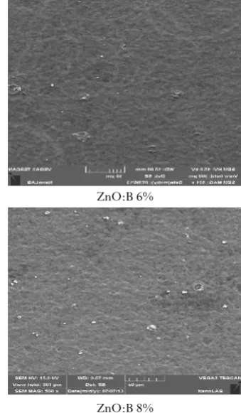
The thin films surface measured by (SEM) showed the upper view morphology of ZnO:B films as shown in images of the figure (5). The grain size of the films decreased with increasing boron doping concentration. The grain size of ZnO:B nanostructured thin films measured by SEM were within the range of (18-37) nm [16, 17].
ZnO
ZnO:B 2%
ZnO:B 4%
ZnO:B 6%
ZnO:B 8%
Figure 5:SEM image of ZnO and ZnO:B nanostructures with concentrations of 2, 4, 6 and 8%.
Sensing properties of NH3 gas:
New materials and treatment processes for applications of gas sensing that can detect gaseous molecules have attracted increasing attention for several years. Several types of gases, such as H2, NH3, CO2, and NO2, are toxic, flammable, or
harmful. Among these gases, NH3 is the most common and is
used in food processing, agriculture, environmental remediation, and medical diagnostics.
The mechanism of sensing of ZnO to NH3 gas depended on the
interactions between the reducing gas and the negatively charged O2− ions on the surface of ZnO thin films, thereby
causing a variation in conductance, as described by the following equation [10]:
2NH3 + 3O2−→ 3H2O + N2 + 3e − (1)
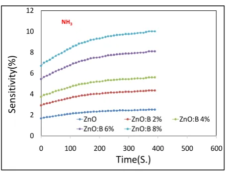
By the electrons released back into the ZnO conduction band and increasing the carrier-doped in the ZnO active layer, the resistance of the thin film was decreased upon exposure to a reducing gas. Figure (6) shows the sensitivity of ZnO and ZnO:B as a function of operating time for NH3 gas at the room
Journal of Advanced Pharmacy Education & Research | Oct-Dec 2019 | Vol 9 | Issue4 27 Figure 6:Sensitivity for ZnO, ZnO:B with doping
concentration 2, 4, 6 and 8%. Deposited on the p-PS substrate as a function of operating time for NH3 gas with a concentration
of 300 ppm at R.T.
Figure (7) shows the sensitivity of ZnO and ZnO:B as a function of operating time for NH3 gas at the room temperature with the
concentration of (300ppm) at R.T. prepared on n-type porous silicon (n-PS) substrate at 450oC. The sensitivity of the films
deposited on n-PS was higher than the sensitivity of the films deposited on p-type porous silicon p-PS due to the negative charge of n-PS. The sensitivity increased with the increase of the concentration of boron due to the increase of electrons in the thin films.
Figure 7:Sensitivity for ZnO, ZnO:B with doping concentration (2, 4, 6 and 8) %. Deposited on the n-PS substrate as a function of operating time for NH3 gas with the
concentration of 300ppm at R.T.
Sensing properties of CO gas:
The sensing mechanism of ZnO towards CO gas depended on the interaction between the reducing gas and the negatively charged O2− ions on the ZnO thin films surface, thereby causing
a variation in conductance, as described by equation [18]:
CO(gas)+ O-(ads)→ CO2 +e- (2)
So that, by the electrons released back into the ZnO conduction band and increasing the carrier-doped in the ZnO active layer, the resistance of the sensor was decreased upon the exposure to a reducing gas [19, 20]. Figure (8) shows the sensitivity of ZnO,
ZnO:B thin films of doping concentrations of (2, 4, 6 and 8)% deposited on the p-PS substrate as a function of operating time for CO gas with the concentration of 300 ppm at room temperature. The sensitivity increased with the increase of Boron concentration due to the increase of boron electrons in the thin films, so that the increase of Boron-doped led to improve the sensitivity [21].
Figure 8:Sensitivity for ZnO, ZnO:B with doping concentration 2, 4, 6 and 8%. Deposited on the p-PS substrate
as a function of operating time for CO gas with the concentration of 300ppm at R.T.
Figure (9) shows the Sensitivity of ZnO, ZnO:B thin films of doping concentrations of 2, 4, 6 and 8% deposited on the n-PS substrate as a function of operating time for CO gas with the concentration of 300 ppm at R.T. The sensitivity was increased with the increase of Boron concentration due to the increase of Boron electrons in the thin films, so that the increasing of Boron-doped led to improve the sensitivity.
Figure 9:Sensitivity for ZnO, ZnO:B with doping concentration (2, 4, 6 and 8) %. Deposited on the n-PS substrate as a function of operating time for CO gas with the
concentration of 300 ppm at R.T.
0 2 4 6 8 10 12
0 100 200 300 400 500 600
ZnO ZnO:B 2% ZnO:B 4%
ZnO:B 6% ZnO:B 8%
Time(S.) Se n sit iv it y(% ) NH3 0 2 4 6 8 10 12
0 100 200 300 400 500
ZnO ZnO:B 2% ZnO:B 4%
ZnO:B 6% ZnO:B 8%
NH3 S e n sit iv it y (% )
Time(S.)
0 0.1 0.2 0.3 0.4 0.5 0.60 200 400 600 800 1000
ZnO ZnO:B 2% ZnO:B 4% ZnO:B 6% ZnO:B 8% S e n si ti vity(% ) Time(s.) CO 0 0.1 0.2 0.3 0.4 0.5 0.6
0 200 400 600 800 1000
28 Journal of Advanced Pharmacy Education & Research | Oct-Dec 2019 | Vol 9 | Issue4
Conclusions
It was found from the results that the increasing of boron concentration in ZnO decreased the grain size and increased the roughness so that the surface area of the interaction of the films increased. The increase of boron concentration increased the sensitivity of the films. The sensitivity of the thin films deposited on the n-PS substrate was higher than the p-PS.
References
1. Hjiri M. Lassaad El. M. Leonard S. G. Donato N. and Neri G., "CO and NO2 Selective Monitoring by ZnO-Based Sensors", Nanomater., 2013, 3(3), 357-369. 2. Kayahan E., "White light luminescence from annealed
thin ZnO deposited porous silicon", Lumin., 2010, 130 (7), pp: 1295–1299.
3. Spitsina S.,"Growth, Doping, and Characterization of ZnO Nanowires: Application in a Miniaturized Gas Ionization Sensor", PhD. Thesis in the Department of Electrical and Computer Engineering, Concordia University, Canada, 2013.
4. Dwivedi V. K. Srivastava P. and Prakash G.V., "Photoconductivity and surface chemical analysis of ZnO thin films deposited by solution-processing techniques for nano and microstructure fabrication", J. Semi, 2013, 34(3), article id. 033001.
5. Spalenka J. W. Gopalan P. Katz H. E. and Evans P. G.,"Electron mobility enhancement in ZnO thin films via surface modification by carboxylic Acids Appl. Phys. Let., 2013, 102, 041602. https://doi.org/10.1063/1.4790155
6. Berestok T.O. Kurbatov D.I. Opanasyuk N.M. and Pogrebnjak A.D. "Structural Properties of ZnO Thin Films Obtained by Chemical Bath Deposition Technique" J. Nano Elect. Phys., 2013, 5 (1):1009. 7. Gültekin D. Alaf M. and Akbulut H., "Synthesis and
Characterization of ZnO Nanopowders and ZnO-CNT Nanocomposites Prepared by Chemical Precipitation Route", Acta Phys. Pol. A., 2013, 123(2), 274-275. 8. Agarwa M. Modi P. and Dusane R.O., "Study of Elect.,
Optical and Structural Properties of Al- Doped ZnO Thin Films on PEN Substrates", J. Nano Elect. Phys., 2013, 5(2), 02027.
9. Khan F. Mobin A. Husain M., "Formation of ZnO by Annealing of Thermally Evaporated Zinc in Oxygen Ambient for Solar Cell Application".International Journal of Electronics and Computer Science Engineering. 1956, 2277, 823-827.
10. Connolly J. R., "Elementary Crystallography for X-Ray Diffraction", 2012, EPS400-002.13 pages.
11. Mondal S. Bhattacharyya S. R. and Mitra P.,"Effect of Al doping on microstructure and optical band gap of ZnO thin film synthesized by successive ion layer adsorption and reaction", Paramana J. Phys., Indian Acad. Sci., 2013, 80 (2), 315–326.
12. Azarooff L.V., "Elementary of X-Ray Crystallography" Mc Graw-Hill Book Company, 1968, 552-556. 13. Wahab H., "Metal oxide catalysts for carbon nanotubes
growth: The growth mechanism using NiO and doped ZnO", PhD. Thesis Department of Electronic, University of York, York, British, 2012.
14. Trunk M., "Novel ZnO-based Ternary Oxides for Optoelectronic Applications", PhD. Thesis, Department of Physics, University of Oslo, Oslo, Norway, 2012.
15. Obata T. Komeda K. Nakao T. Ueba H., and Tasygama C.," Structural characterization of Si0.7Ge0.3 layers grown on Si(001) substrates by molecular beam epitaxy " J. Appl. Phys., 1997, 81 , 199-204.
16. Kumarb V. Singh R.G. Singh N. Kapoor A. Mehra R.M. and Purohit L.P., "Synthesis and characterization of aluminum–boron co-doped ZnO nanostructures", Mate. Res. Bull., 2013, 48 (2), 362–366.
17. Rashid Hashim Jabbar, " Study the Physical Properties of Aluminum and Boron co-doped Zinc Oxide Thin Films as Gas Sensor for NH3 and NO2 ", PhD. Thesis, Al – Mustansiriyah University, College of Science, 2015.
18. Prajapati C.S. Kushwaha A. and Sahay P.P., "Effect of Al dopants on the structural, optical and gas sensing properties of spray-deposited ZnO thin films", Materials Chemistry and Physics, 142 (1), Pages 276-285.
19. Jarrah R. M. Sh.. "Fabrication and Characteristics Study of ZnO/Si Heterojunction by DC Magnetron Sputtering", A thesis, Univ. Baghdad, Coll. Sci., Dep. Phys., Baghdad, Iraq, 2013.
20. Ioannis Kortidis, Hendrik C. Swart, Suprakas Sinha Ray, David E. Motaung, " Detailed understanding on the relation of various pH and synthesis reaction times towards a prominent low temperature H2S gas sensor based on ZnO nanoplatelets", https://www.researchgate.net/publication/33087327 9, 2019.