N A N O E X P R E S S
Open Access
Investigation on the passivated Si/Al
2
O
3
interface
fabricated by non-vacuum spatial atomic layer
deposition system
Shui-Yang Lien
1, Chih-Hsiang Yang
2, Kuei-Ching Wu
3and Chung-Yuan Kung
2*Abstract
Currently, aluminum oxide stacked with silicon nitride (Al2O3/SiNx:H) is a promising rear passivation material for high-efficiency P-type passivated emitter and rear cell (PERC). It has been indicated that atomic layer deposition system (ALD) is much more suitable to prepare high-quality Al2O3films than plasma-enhanced chemical vapor deposition system and other process techniques. In this study, an ultrafast, non-vacuum spatial ALD with the deposition rate of around 10 nm/min, developed by our group, is hired to deposit Al2O3films. Upon post-annealing for the Al2O3films, the unwanted delamination, regarded as blisters, was found by an optical microscope. This may lead to a worse contact within the Si/Al2O3interface, deteriorating the passivation quality. Thin stoichiometric silicon dioxide films prepared on the Si surface prior to Al2O3fabrication effectively reduce a considerable amount of blisters. The residual blisters can be further out-gassed when the Al2O3films are thinned to 8 nm and annealed above 650°C. Eventually, the entire PERC with the improved triple-layer SiO2/Al2O3/SiNx:H stacked passivation film has an obvious gain in open-circuit voltage (Voc) and short-circuit current (Jsc) because of the increased minority carrier lifetime and internal rear-side reflectance, respectively. The electrical performance of the optimized PERC with theVocof 0.647 V, Jscof 38.2 mA/cm
2
, fill factor of 0.776, and the efficiency of 19.18% can be achieved.
Keywords:PERC; Non-vacuum spatial atomic layer deposition; Al2O3/SiNx:H stacked rear passivation; Blister; Triple-layer SiO2/Al2O3/SiNx; H stacked passivation films
Background
For the past decade years, dielectric films have become promising materials applied in high-efficiency silicon solar cells due to their superior surface passivation ef-fect. An attractive candidate for outstanding Si surface passivation is aluminum oxide (Al2O3), which can be de-posited by physical vapor deposition (PVD) system [1], chemical vapor deposition (CVD) system [2-4], liquid-phase deposition (LPD) technique [5,6], and atomic layer deposition (ALD) system [7-9]. Generally, ALD system is the most suitable choice for the deposition of Al2O3 owing to some advantages: (i) capable of producing very thin conformal and uniform films, (ii) with large pro-cess temperature window, and (iii) able to deposit films on high-aspect-ratio substrates. However, traditional
plasma-assist ALD and thermal ALD have an extremely low de-position rate of the order of dozen picometers per second; the industrial application of this technique is chiefly lim-ited to CMOS and DRAM processes [10]. Recently, Al2O3 films are applied to a noted cell structure so-called passiv-ated emitter and rear cell (PERC) as the passivation layers. The PERC structure which offers the possibility of import-antly improved performance over traditional commercial cell design needing only little extra process steps can achieve the efficiency of around 22%. Hence, the PERC structure is going to be the next key product of most solar companies.
For the solar industrials, the deposition of Al2O3for PERC is mainly by turn-key plasma-enhanced chemical vapor deposition (PECVD) technique due to its higher production capacity in comparison with ALD system. But the uniformity of the PECVD Al2O3 films is diffi-cult to control well, making the film thicker at the cen-tral region and thinner around the edge of the wafer. A * Correspondence:[email protected]
2
Department of Electrical Engineering, National Chung Hsing University, 250 State Road, Taichung 402, Taiwan
Full list of author information is available at the end of the article
spatial-type ALD with both merits of a high deposition rate and producing films with a high-level uniformity has been proposed to provide a great passivation effect and enhance the production capacity. The precursor TMA (Al(CH3)3) and reactant water vapor (H2O) were used to proceed two half reactions to deposit the Al2O3 films in spatial ALD. A little amount of hydrogen (H2) and H2O may remain on the rear-side surface of Si sub-strate. The blisters which form at the Si/Al2O3interface occur under an external load in the presence of a ten-sile residual stress due to the effusion of H2 and H2O [11]. The blistering may deteriorate minority carrier lifetime. Several studies have claimed that treating the Al2O3 films with enough thermal budgets prior to the capping of SiNx:H and thinning the thickness Al2O3film are two possible ways to conquer this obstacle [12].
In this study, a non-vacuum spatial ALD with a de-position rate of 10 nm/min which is ten times faster than the traditional ALD systems is developed. The fast-growing Al2O3films are used as a rear-side passivation layer applied to the P-type PERC structure. In the begin-ning, the analysis of electrical and structural properties for pure Al2O3is characterized. The expected blistering formation is observed through an optical microscope. Two approaches tried to solve the blistering problem as well as to improve the efficiency of PERC. Firstly, a very thin stoichiometric silicon dioxide (SiO2) film deposi-ted by inductively coupled plasma chemical vapor depo-sition (ICPCVD) is inserted into the interface between Al2O3and silicon wafer to reduce blisters. In the mean-time, SiO2 film can further chemically passivate the interface defects. Secondly, reducing the thickness of the Al2O3 film to lower than 10 nm and increasing the post-annealing temperature to a higher tempera-ture of 650°C to enhance out diffusion of gas. After that, the SiNx:H films with abundant hydrogen con-tent prepared by ICPCVD are capped on the Al2O3 films to enhance the passivation effect by filling dangling bonds. The positive effect of the stacked passivation layer is proven from a quasi-steady-state photo-conductance (QSSPC). The electrical performance for the PERC devi-ces with various rear-side-passivated structures is even-tually investigated.
Methods
Few pieces of 15.6 cm × 15.6 cm shiny etched Cz-Si wa-fers (P-type, 5 Ω-cm, (100-oriented)) wafers of 200 μm thick were prepared. They were then etched in a chem-ical polishing solution to remove the saw damages at the edges followed by standard RCA clean. Subsequently, the identical Al2O3films were deposited on both sides of the Si wafers to evaluate the passivation effect. Various thicknesses of the Al2O3 films from 10 to 25 nm were firstly prepared before sending them to the furnace for
post-annealing process in N2ambient. The temperature was set from 450°C to 600°C. We prepared other wafers capped with identical thin SiO2films as an interlayer by ICPCVD. The Al2O3films were deposited on the top of SiO2films to form stacked structures. Those samples were also annealed in the range from 450°C, 500°C, 550°C, to 600°C, respectively. For a special case, the stacked struc-tures SiO2/Al2O3with thinner Al2O3of about 8 nm were fabricated for comparison. A higher annealing tempera-ture of 650°C was treated on these samples to drive more imbedded gas out diffused. The stacked structures capped with silicon nitride films doped hydrogen (SiNx:H) was made by ICPCVD, forming the triple-layer stacked struc-ture of SiO2/Al2O3/SiNx. These triple-layer stacked films were then annealed at 450°C for 20 min.
High-resolution scanning electrical microscope (HR-SEM) and optical microscope (OM) were used to observe the thicknesses of the Al2O3films and the distribution of blisters, respectively. The wafers were characterized by QSSPC effective lifetime measurement (Sinton Company WCT-120; Sinton Instruments, Boulder, CO, USA). Cross-sectional images of the stacked films were carried out by transmission electron microscope (TEM).
Results and discussion
Figure 2a shows the HR-SEM images for various cycles of deposition of the Al2O3films including 50, 100, 300, and 400 cycles. The regime marked by a double-sided arrow is the Al2O3 film. The aim of capping the SiNx film on the Al2O3film is to discriminate each layer to be observed clearly. From this figure, it can be seen that under different deposition cycles, all the Al2O3films are uniform without any rough morphology on the surface, revealing the feasibility and reproducibility of this ALD system. Thicknesses of 10.3, 34.8, 48.8, and 62.6 nm cor-respond to 50, 200, 300, and 400 cycles, respectively. The ALD process allows the deposition of Al2O3 films with an accurate thickness control is demonstrated in Figure 2b. It is shown that the Al2O3 film thickness scales near linear with the number of ALD cycles for
our non-vacuum spatial ALD. The slope in Figure 2b is defined as growth per cycle (GPC). The GPC here is around 0.16 nm/cycle, 1 s per cycle, so that the depos-ition rate is around 10 nm/min. Compared to traddepos-itional plasma-enhanced ALD and thermal ALD, the deposition rate of 10 nm/min is much faster, displaying its high po-tential for being used in the industrials.
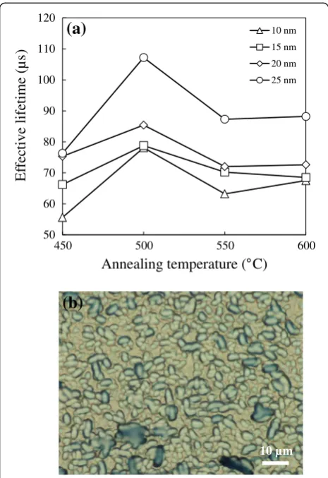
[image:3.595.61.536.87.349.2]The recombination rate at the Si wafer surface is nor-mally controlled by the excess concentration of minority carriers near the surface. Minimizing the concentration of minority concentration thus reduces the surface re-combination rate. Figure 3 shows the minority carrier lifetime for various Al2O3 film thicknesses with 10 to 25 nm annealed at 450°C to 600°C in the N2 ambient. As can be seen in Figure 3, the trends of lifetime for all curves are almost the same, increasing with the in-crease of temperature firstly and decreasing after at the annealing temperature of 500°C. The decreased lifetime after 500°C can be explained that little bonding struc-ture is broken, releasing few dangling bonds to trap mi-nority carriers. On the other hand, as the thickness of the Al2O3 film increases, the minority carrier lifetime increases as well. This can be attributed to a lower in-terface defect density deduced from capacitance voltage measurement for a thicker Al2O3 film [13]. The peak lifetime 85.5μs is achieved (the lifetime of bare wafer is
Table 1 Detailed thickness information of rear-side passivation films
Cell type
SiO2(nm) Al2O3(nm) SiNx:H (nm) Annealing temperature prior to cap SiNx:H (°C)
A N/A 25 N/A 500
B 3 25 N/A 500
C 3 8 N/A 650
D 3 8 70 650
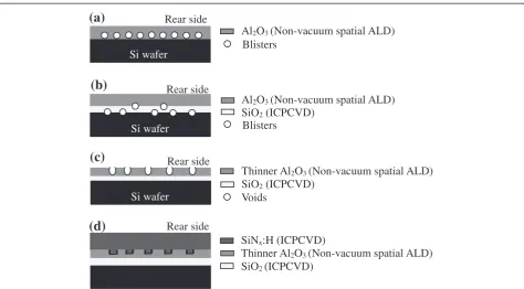
(a)
Blisters
(d)
Al2O3 (Non-vacuum spatial ALD)
Si wafer
(c)
Blisters
Si wafer
SiO2(ICPCVD)
(b)
Si wafer
Al2O3(Non-vacuum spatial ALD)
Thinner Al2O3(Non-vacuum spatial ALD)
SiO2(ICPCVD)
Rear side
Voids
Thinner Al2O3(Non-vacuum spatial ALD)
Rear side Rear side
SiO2(ICPCVD)
SiNx:H (ICPCVD) Si wafer
Rear side
[image:3.595.57.290.655.733.2]about 5 μs), while the thickness of the Al2O3 film is 25 nm and the annealing temperature is 500°C.
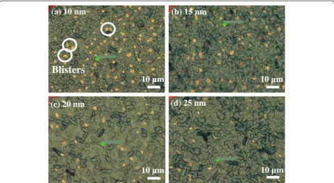
In most cases, blister formation caused by the effusion of H2O and H2 from the silicon bulk may occur upon post-annealing step. Those unwanted blisters are re-garded as defects, deteriorating both the chemical effect and field effect of the Al2O3films [14]. Figure 4 displays the optical microscope images for different thicknesses of the Al2O3 film annealed at 500°C: (a) 10 nm, (b) 15 nm, (c) 20 nm, and (d) 25 nm. All the samples have a large number of blisters shown as little spots highlighted by a circle symbol. The diameters of the blister are uni-form in the range of 3 ~ 4 μm. With the increase of
thickness, the blister density goes lower, resulting in a better passivation effect. The phenomenon can be ex-plained in terms of two aspects: (i) as the Al2O3 films deposited layer by layer, the weight of entire films be-comes heavier, making the blister under the Al2O3films dissipate literally; (ii) one Al2O3layer forms via the reac-tion between TMA and H2O in sequence on the surface of the silicon wafer. After dozens of cycles, the chem-ical reaction tends to be stable. The usage of H2O raises due to its up and down movement among each porous Al2O3 layer and chemical reaction with residual TMA at the bottom of the Al2O3films. Hence, the amount of the blisters decreases with an increase of the thickness of the Al2O3. Simultaneously, the distribution of blis-ters can also be an evidence to account for the lifetime trend in Figure 3.
The blister-blocking effect of SiO2 on silicon can be reflected in Figure 5. Figure 5a shows the minority car-rier lifetime for 3 nm of the SiO2films capped with vari-ous Al2O3films thicknesses of 10 to 25 nm annealed at 450°C to 600°C in the N2 ambient. Compared to the trend of Figure 3, it almost maintains unchanged, but the average lifetime of all samples has a little increase. The peak value of 107.2 μs is obtained still when the thickness of the Al2O3film is 25 nm, and the annealing temperature is 500°C. The increase of 21.7 μs between two peak lifetime values can be attributed to the enor-mous reduction of blisters, as shown in Figure 5b. The major reason to support SiO2 film to be our option is that the SiO2film has more stoichiometric configuration compared to native oxide (SiOx). When the Al2O3films 0
10 20 30 40 50 60 70
50 100 150 200 250 300 350 400
Number of ALD cycles
T
h
ickn
es
s (nm
)
SiNx:H Al2O3
(a)
[image:4.595.57.293.89.473.2](b)
Figure 2HR-SEM images for various cycles of deposition and
deposition rate of non-vacuum spatial ALD. (a)HR-SEM images
for various cycles of deposition of Al2O3films including 50, 200, 300, and 400 cycles and(b)deposition rate of non-vacuum spatial ALD. This figure can verify the basic characteristic of deposition rate for a self-developed non-vacuum spatial ALD. The image also shows the uniformity of the Al2O3films, revealing its reproducibility.
40 50 60 70 80 90
450 500 55 00
10 nm 15 nm 20 nm 25 nm
Annealing temperature ( C)
Ef
fective lifetime (µ
[image:4.595.306.539.89.279.2]s)
Figure 3Minority carrier lifetime for various thicknesses.
deposited directly on the silicon substrate without SiO2 films as interlayers, the oxygen atom of reactant H2O tends to bond with SiOx to form the stable SiO2; thus, the released H2and residual H2O may probably become the blisters after post-annealing process. The highly stoi-chiometric ICPCVD-SiO2 films inserted into the in-terface between the Al2O3 and silicon wafer effectively prevent the considerable amount of blisters from occur-ring. In addition, several studies have claimed that SiO2 film is a good candidate for chemical passivation to eliminate the dangling bonds on the surface of silicon wafer [15,16]. Also, it can help the Al2O3 films to rear-range their negative fixed charge distributed near the SiO2/Al2O3interface [17,18].
For further improvement for the blistering problem, we reduce the thickness of Al2O3to lower than 10 nm and increase the annealing temperature to 650°C, giving an enough thermal budget prior to the capping of the SiNx:H film. The out-gassing phenomenon can be found. Here, the blister number can further decrease, approa-ching near blister free. Some voids existing within the Al2O3film are caused by the out-gassing effusion. How-ever, the subsequent deposition of SiNx:H prepared by ICPCVD would provide abundant hydrogen atoms to fill the dangling bonds via the voids. The post-anneal (450°C for 20 min) performed after the deposition of SiNx:H is able to activate the passivation of the triple-layer stacked structure [19]. Figure 6 shows the injection
level dependent minority carrier lifetime for the stacked passivation film of Si/3 SiO2/8 Al2O3/70 SiNx:H film and of Si/3 SiO2/6 Al2O3/70 nm-SiNx:H film. The effective lifetime is calculated from the photoluminescence intensity by the self-consistent calibra-tion method proposed by Trupke et al. [20]. Both the triple-layer stacked films have the same structure except the thickness of the Al2O3 film. The former one has a higher average lifetime of 315 μs compared to the latter one of 147 μs. Two major factors, negative fixed charge and blisters, are found to influence the lifetime of the Al2O3 films. Generally, reducing the thickness of the Al2O3films to lower than 10 nm and increasing a post-annealing temperature to higher than 650°C can make blisters out-gassed. In this case, both 6- and 8-nm Al2O3 films are blister free, indicating the lifetime is determined only by negative fixed charge. According to our previous research and some references [21,22], the negative fixed charge may accumulate to enhance the passivation effect as the thickness increases. Hence, the sample with an 8-nm-thick Al2O3layer has a higher lifetime, displaying stronger field-effect passivation than the sample with a 6-nm-thick Al2O3 layer. The optimized lifetime of 315 μs is about three times higher than 107.2μs of the stacked film without SiNx:H. Note that the thickness of the Al2O3within the triple-layer stacked film is reduced to lower than 10 nm, decreasing its field-effect pas-sivation. However, according to some investigation of
10 µm
10 µm
10 µm
(c) 20 nm
(d) 25 nm
(a) 10 nm
(b) 15 nm
Blisters
[image:5.595.58.538.89.352.2]10 µm
[23-26], they demonstrate that a thin Al2O3 of about 10 nm is still sufficient for providing an excellent level of surface passivation. Despite the field-effect passiv-ation may become weaker in this case, the chemical passivation from SiNx:H dominates the whole perform-ance strongly. For a short summary, hydrogen atom in-deed plays a critical role in combing with the Al2O3 film as the passivation stacks.
Figure 7 displays the high-resolution transmission elec-tron microscope (HR-TEM) cross-sectional image of the stacked Si/3 nm-SiO2/8 nm-Al2O3/70 nm-SiNx:H film, in which we can see the three interfaces such as Si/SiO2, SiO2/Al2O3, and Al2O3/SiNx:H are all flattened without any vacancy or void to deteriorate the passivation effect. The very thin SiO2film with only 3 nm is deposited using the ICPCVD. The accurate control in thickness is based on the deposition rate determined by the past experi-ments. In the meanwhile, this TEM image confirms that the Al2O3 film deposited by self-developed non-vacuum spatial ALD is quite uniform.
Figure 8 shows the reproducible illuminated I-V curves and performance of PERC cells for the four kinds of rear-side passivation structure including cell (A) pure 25 nm-Al2O3film, (B) 3 nm-SiO2/25 nm-Al2O3stacked film, (C) 3 nm-SiO2/8 nm Al2O3 film without capping SiNx:H treated with an annealing temperature of 650°C, and (D) 3 nm-SiO2/8 nm Al2O3film/70 nm-SiNx:H trea-ted with an annealing temperature of 450°C for 20 min after the capping of SiNx:H. All the detailed external parameters are summarized in Table 2. We can find that the electrical performance of cells A and B are al-most the same, only with a slight difference in open-circuit voltage (Voc). To understand the performance Voc, we investigate the behavior of minority carrier life-time of the P-type Si wafer. B. Michl et al. have claimed that the excess carrier lifetime substantially affects the 50
60 70 80 90 100 110 120
450 500 550 600
10 nm 15 nm 20 nm 25 nm
Annealing temperature ( C)
Ef
fective lifetime (µ
s)
(a)
(b)
[image:6.595.57.290.88.427.2]10 µm
Figure 5The blister-blocking effect of SiO2on silicon. (a)Minority carrier lifetime for 3 nm SiO2films capped with various Al2O3film thicknesses of 10 to 25 nm annealed at 450°C to 600°C in N2ambient and(b)optical microscope image for 3 nm-SiO2/25 nm-Al2O3stacked film annealed at 500°C N2ambient.
Ef
fective lifetime
(s)
Injection level (cm-3)
0.0E+00 5.0E-05 1.0E-04 1.5E-04 2.0E-04 2.5E-04 3.0E-04 3.5E-04
5.0E+14 5.0E+15 5.0E+16
[image:6.595.56.291.493.695.2]Stacked film with 6nm aluminum oxide Stacked film with 8nm aluminum oxide (cell D)
Figure 6Injection level dependent minority carrier lifetime for
the stacked passivation film.Si/3 nm-SiO2/8 nm-Al2O3/70 nm-SiNx:H
film and Si/3 nm-SiO2/6 nm-Al2O3/70 nm-SiNx:H film.
Figure 7High-resolution transmission electron microscope
(HR-TEM) cross-sectional image of the stacked Si/3 nm-SiO2/8
[image:6.595.304.538.546.697.2]Vocin multi-crystalline materials [27]. Three equations which can describe the relation between minority car-rier lifetime andVoccan be expressed by:
VOC ¼ kTq In J JSC
os þ Job þ
1
ð1Þ
Job ¼ q n 2
i
NA
Dn
Wp − Xp 1 þ
Dn= Wp − Xp
Sback
−1
ð2Þ
1
τeff ¼
1
τbulk þ
Sfront þ Sback
W ð3Þ
where Joe and Job are the reverse saturation current,
respectively. NA is doping concentration, ni is the
in-trinsic carrier concentration,Sbackis the recombination
velocity of back side surface, andτeffandτbulkare effective
lifetime and bulk lifetime of devices, respectively. By Equation3, we can obtain thatSbackmay decrease with
the increase of effective lifetime. Whereas the smaller
Sbackleads to a lowerJobexpressed in Equation2.
Gen-erally, the value of Jobchanges its order of magnitude,
leading to a huge variation ofVoc. Hence, from Equation
1, an increasedVoccan be obtained by a reducedJob. The
deposition of very thin SiO2film in cell B can not only
re-duce the blister number but also help to rearrange the negative fixed charge near the surface of the Al2O3film,
thus improving the minority carrier lifetime. According to the explanation above, the higher lifetime of cell B leads to a higher Voc. As for cell C, it can be seen that
all the electrical performances are the worst, especially in fill factor (FF). The factor to influence FF in a solar diode is the contact resistance between metal and semi-conductor [28,29]. The blisters in cell C are almost out-gassed, resulting in random distribution of voids. After the laser ablation for the rear contact fabrication, the non-uniform openings can be obtained, forming an un-favorable rear contact. The following high series con-tact may bring a huge reduction in FF. In comparison with cells A, B, and C, cell D has the apparent improve-ment in Voc and short-circuit current (Jsc). The
triple-layer stacked film combines the chemical passivation with field-effect passivation at the same time, leading to a relatively high lifetime of 315 μs. Thus, an optimized
Voccan be acquired. As to the highJsc, this can be
ex-plained that an optimized rear-side triple-layer stacked passivation also acts as an excellent internal back side reflective coating. By reflecting more long-wavelength light, there is an obvious gain inJsc[30]. The final
opti-mal efficiency of the cell D achieves 19.18%.
Conclusions
In this study, the uniform Al2O3 films with high repro-ducibility are fabricated by self-developed non-vacuum spatial ALD system. We report two effective ways to im-prove the blistering problem upon the annealing after the deposition of Al2O3, including (i) depositing a thin stoichiometric SiO2 film on the surface of the silicon wafer by ICPCVD and (ii) further reducing the thickness of the Al2O3 film to below 10 nm and provide higher thermal budget to the stacked Si/SiO2/Al2O3film prior to capping with SiNx:H. An obvious improvement on blistering issue can be verified from OM images and minority carrier lifetime measurement. The blisters can be out-gassed when treating the 8-nm thin Al2O3film with a 650°C annealing temperature. The subsequent deposition of 70 nm-SiNx:H film can not only protect the Al2O3film from damage but also provide an effec-tive chemical passivation on the surface of the silicon wafer via the voids. The improved triple-layer stacked Si/3 nm-SiO2/8 nm-Al2O3/70 nm-SiNx:H passivation film is successfully applied to PERC device with distinct gains in Vocof about 0.03 V and in Jsc of about 0.6 mA/cm2. The final optimal conversion efficiency of 19.18% for the PERC device with the improved stacked passivation film is obtained.
Voltage (V)
Current densit
y
(mA/c
m
2 )
0 5 10 15 20 25 30 35 40 45
0 0.1 0.2 0.3 0.4 0.5 0.6 0.7 Cell A
Cell B
[image:7.595.56.291.88.278.2]Cell C Cell D
[image:7.595.55.290.663.734.2]Figure 8Reproducible illuminated I-V curves and performance of PERC cells for four PERC structures.
Table 2 Photovoltaic performance for PERC cells with various rear-side passivation films
Cell type Voc(V) Jsc(mA/cm2) FF Efficiency (%)
A 0.619 37.6 0.78 18.15
B 0.623 37.7 0.782 18.36
C 0.618 37.2 0.748 17.2
Abbreviations
ARC:anti-reflective coatings; ALD: atomic layer deposition system; CVD: chemical vapor deposition system; FF: fill factor; GPC: growth per cycle; HR-SEM: resolution scanning electron microscopy; HR-TEM: high-resolution transmission electron microscope; ICPCVD: inductively coupled plasma chemical vapor deposition; LPD: liquid-phase deposition technique; Voc: open-circuit voltage; PERC: passivated emitter and rear cell; PVD: physical vapor deposition system; QSSPC: quasi-steady-state photo-conductance; Jsc: short-circuit current; TEM: transmission electron microscope.
Competing interests
The authors declare that they have no competing interests.
Authors’contributions
SYL led the experimental and analytical efforts on the passivation effect of various stacked passivation films of PERC. CHY assisted in optimizing the performance of various stacked passivation films and drafted the manuscript. KCW assisted in fabricating the complete PERC. CYK contributed to the design and analysis of the experiments for the stacked passivation films and integrated the comments from all authors. All authors read and approved the final manuscript.
Authors’information
SYL is currently an Associate Professor in the Department of Materials Science and Engineering, DaYeh University, Changhua, Taiwan. He has done work in the field of solar cell materials by plasma-enhanced chemical vapor deposition and hot-wire chemical vapor deposition. CHY is presently a Ph.D. student at the Department of Electrical Engineering, National Chung Hsing University, Taichung, Taiwan, R.O.C., majoring high-efficiency mono-crystalline silicon solar cells. KCW is the leader of Crystalline Silicon R & D. Section, Mosel Vitelic Inc., Taiwan, R.O.C. CYK received the Ph.D. degree from the Department of Materials Science and Engineering, Northwestern University, Evaston, IL, USA in 1978. He has been working as staff scientist in Lawrence Berkeley Laboratory for 2 years and ITRI Hsinchu, Taiwan for 4 years. Currently, he is a Professor in the Department of Electrical Engineering, National Chung Hsing University, Taiwan. His research interests include the synthesis and application of semiconductor materials.
Acknowledgements
This work is sponsored by Mosel Vitelic Inc., Taiwan, R.O.C. and the Ministry of Science and Technology of the Republic of China under the grants No. 102-2221-E-212-021-MY2 and Hsinchu Science Park Bureau, Ministry of Science and Technology, Republic of China under the grants No. 102A24.
Author details
1Department of Materials Science and Engineering, DaYeh University, No. 168, Xuefu Road, Changhua 515, Taiwan.2Department of Electrical Engineering, National Chung Hsing University, 250 State Road, Taichung 402, Taiwan.3Crystalline Silicon R & D Section, Mosel Vitelic Inc, No. 1, Creation Road 1, Hsinchu 300, Taiwan.
Received: 16 November 2014 Accepted: 5 February 2015
References
1. Li TA, Ruffell S, Tucci M, Mansoulie’Y, Samundsett C, DeIullis S, et al. Influence of oxygen on the sputtering of aluminum oxide for the surface passivation of crystalline silicon. Sol Energ Mat Sol C. 2011;95:69–72. 2. Maruyama T, Nakai T. Aluminum oxide thin films prepared by chemical
vapor deposition from aluminum 2-ethylhexanoate. Appl Phys Lett. 1991;58:2079–80.
3. Klein TM, Niu D, Epling WS, Li W, Maher DM, Hobbs CC, et al. Evidence of aluminum silicate formation during chemical vapor deposition of amorphous Al2O3thin films on Si (100). Appl Phys Lett. 1999;75:4001–3. 4. Tristant P, Ding Z, Trang Vinh QB, Hidalgo H, Jauberteau JL, Desmaison J,
et al. Microwave plasma enhanced CVD of aluminum oxide films: OES diagnostics and influence of the RF bias. Thin Solid Films. 2001;390:51–8. 5. Sun J, Sun YC. Chemical liquid phase deposition of thin aluminum oxide
films. Chinese J Chem. 2004;22:661–7.
6. Basu S, Singh PK, Huang JJ, Wang YH. Liquid-phase deposition of Al2O3thin films on GaN. J Electrochem Soc. 2007;154:H1041–6.
7. Hoex B, Schmidt J, Bock R, Altermatt PP, van de Sanden MCM, Kessels WMM. Excellent passivation of highly doped p -type Si surfaces by the negative-charge dielectric Al2O3. Appl Phys Lett. 2007;91:112107–112107–3. 8. Benick J, Hoex B, van de Sanden MCM, Kessels WMM, Schultz O, Glunz SW.
High efficiency n-type Si solar cells on Al2O3-passivated boron emitters. Appl Phys Lett. 2008;92:253504–253504–3.
9. Dueñas S, Castán H, García H, de Castro A, Bailón L, Kukli K, et al. Influence of single and double deposition temperatures on the interface quality of atomic layer deposited Al2O3dielectric thin films on silicon. Appl Phys Lett. 2006;99:054902–054902–8.
10. Poodt P, Lankhorst A, Roozeboom F, Spee K, Maas D, Vermeer A. High-speed spatial atomic-layer deposition of aluminum oxide layers for solar cell passivation. Adv Mater. 2010;22:3564–7.
11. Bart V, Hans G, Veerle S, Ingrid DW, Johan M, Shuji T, et al. A study of blister formation in ALD Al2O3grown on silicon. In: PVSC’38: 38th Photovoltaic Specialists Conference IEEE, June 2012; Austin. Published by IEEE, New York; 2012. 1135–1138
12. Hennen L, Granneman EHA, Kessels WMM. Analysis of blister formation in spatial ALD Al2O3for silicon surface passivation. In: PVSC’38: 38th Photovoltaic Specialists Conference IEEE, June 2012; Austin. Published by IEEE, New York; 2012. 1049–1054
13. Saint-Cast P, Heo YH, Billot E, Olwa P, Hofmann M, Rentsch J, et al. Variation of the layer thickness to study the electrical property of PECVD Al2O3/c-Si interface. Energy Procedia. 2011;8:642–7.
14. Saint-Cast P, Kania D, Heller R, Kuehnhold S, Hofmann M, Rentsch J, et al. High-temperature stability of c-Si surface passivation by thick PECVD Al2O3with and without hydrogenated capping layers. Appl Surf Sci. 2012;258:8371–6.
15. Sameshima T, Sakamoto K, Tsunoda Y, Saitoh T. Improvement of SiO2 properties and silicon surface passivation by heat treatment with high-pressure H2O vapor. Jan J Appl Phys. 1998;37:L1452–4.
16. Schmidt J, Kerr M, Cuevas A. Surface passivation of silicon solar cells using plasma-enhanced chemical-vapour-deposited SiN films and thin thermal SiO2/plasma SiN stacks. Semicond Sci Technol. 2001;16:164–70.
17. Agostinelli G, Delabie A, Vitanov P, Alexieva Z, Dekkers HFW, Wolf SD, et al. Very low surface recombination velocities on p-type silicon wafers passivated with a dielectric with fixed negative charge. Sol Energ Mat Sol C. 2006;90:3438–43.
18. Gielis JJH, Hoex B, van de Sanden MCM, Kessels WMM. Negative charge and charging dynamics in Al2O3films on Si characterized by second-harmonic generation. J Appl Phys. 2008;104:073701–073701–5.
19. Dingemans G, van de Sanden MCM, Kessels WMM. Excellent si surface passivation by low temperature SiO2using an ultrathin Al2O3capping film. Phys Status Solidi-R. 2011;5:22–4.
20. Trupke T, Bardos RA, Abbott MD. Self-consistent calibration of photoluminescence and photoconductance lifetime measurements. Appl Phys Lett. 2005;87:184102–184102–3.
21. Boris V, Florian W, Dimitri Z, Rolf B, Jan S. Comparison of the thermal stability of single Al2O3layers and Al2O3/SiNxstacks for the surface passivation of silicon. Energy Procedia. 2011;8:307–12.
22. Teng YW, Cheng CL, Chien HH, Chen HD, Chung YK. Effect of annealing on aluminum oxide passivation layer for crystalline silicon wafer. J Energy Power Eng. 2013;7:1505–10.
23. Black LE, Allen T, McIntosh KR, Cuevas A. Effect of boron concentration on recombination at the p-Si–Al2O3interface. Appl Phys Lett. 2014;115:093707–093707–9.
24. Duttagupta S, Lin F, Shetty KD, Wilson M, Ma FJ, Lin JJ, et al. State-of-the-art surface passivation of boron emitters using inline PECVD AlOx/SiNxstacks for industrial high-efficiency silicon wafer solar cells. In: PVSC’38: 38th Photovoltaic Specialists Conference IEEE, June 2012; Austin. Published by IEEE, New York; 2012. 1036–1039
25. Wu J, Liu YY, Wang XS, Zhang LJ. Application of ion implantation emitter in PERC solar cells. IEEE J Photovoltaics. 2014;4:52–7.
26. Hoex B, Gielis JJH, van de Sanden MCM, Kessels WMM. On the c-Si surface passivation mechanism by the negative-charge-dielectric Al2O3. J Appl Phys. 2008;104:113703–113703–7.
28. Gatz S, Dullweber T, Brendel R. Evaluation of series resistance losses in screen-printed solar cells with local rear contacts. IEEE J Photovoltaics. 2011;1:37–42.
29. Meier DL, Good EA, Garcia RA, Bingham BL, Yamanaka S, Chandrasekaran V, et al. Determining components of series resistance from measurements on a finished cell. In: Photovoltaic Energy Conversion, Conference Record of the 2006 IEEE 4th World Conference on (Volume 2), May 2006; Waikoloa. Published by IEEE, New York; 2006. 1315–1318
30. Lin JW, Chen YY, Gan JY, Hseih WP, Du CH, Chao TS. Improved rear-side passivation by atomic layer deposition Al2O3/SiNxstack layers for high VOC industrial P-type silicon solar cells. IEEE Electr Device L. 2013;34:1163–5.
Submit your manuscript to a
journal and benefi t from:
7Convenient online submission 7Rigorous peer review
7Immediate publication on acceptance 7Open access: articles freely available online 7High visibility within the fi eld
7Retaining the copyright to your article