N A N O E X P R E S S
Open Access
Structural and electronic properties of
two-dimensional stanene and graphene
heterostructure
Liyuan Wu
1, Pengfei Lu
1,4*, Jingyun Bi
1, Chuanghua Yang
2, Yuxin Song
4, Pengfei Guan
3*and Shumin Wang
4,5Abstract
Structural and electronic properties of two-dimensional stanene and graphene heterostructure (Sn/G) are studied by using first-principles calculations. Various supercell models are constructed in order to reduce the strain induced by the lattice mismatch. The results show that stanene interacts overall weakly with graphene via van der Waals (vdW) interactions. Multiple phases of different crystalline orientation of stanene and graphene could coexist at room temperature. Moreover, interlayer interactions in stanene and graphene heterostructure can induce tunable band gaps at stanene’s Dirac point, and weak p-type and n-type doping of stanene and graphene, respectively, generating a small amount of electron transfer from stanene to graphene. Interestingly, for model Snpffiffiffi7=G 5ð Þ, there emerges a band gap about 34 meV overall the band structure, indicating it shows semiconductor feature.
Keywords:First-principles, Stanene, Graphene, Heterostructure, Structural properties
Background
Two-dimensional (2D) materials, such as graphene [1–6],
silicene [7–13], germanene [14–16], hexagonal boron
ni-tride (hBN) [17, 18], and transition metal dichalcogenides
(TMDs, such as MoS2) [19, 20], have received considerable
attention recently because of their outstanding properties and potential applications. These 2D layers can be inte-grated into a multilayer stack (vertical 2D heterostructure) and have been widely studied experimentally and theoretic-ally, such as graphene/silicene (G/Si) [21, 22], graphene/ hexagonal boron nitride (G/hBN) [23, 24], silicene/HBN [25], silicene/GaS [26, 27], TMDCs/graphene [28, 29], stacked TMDCs [30, 31], phosphorene/MoS2 [32], and phosphorene/graphene [33]. The resulting artificial 2D het-erostructures provide access to new properties and applica-tions far beyond their simplex components.
Most recently, a new 2D material, stanene (the form of 2D stannum), firstly proposed by Liu et al. [34], has been mentioned as a host material for topological insulator (TI), which are new states of quantum matter with an insulating
bandgap in the bulk while conducting states at the edges
and protected by time reversal symmetry [35–40]. For
in-stance, stanene and its derivatives could support a large-gap 2D quantum spin Hall (QSH) state and thus enable the dissipation less electric conduction at room temperature. Moreover, stanene could also provide enhanced thermo-electricity [41], topological superconductivity [42], and the near-room-temperature quantum anomalous Hall (QAH) effect [43]. Zhu et al. [41] have reported the successful
fab-rication of 2D stanene with metallic features on the Bi2Te3
(111) substrate by molecular beam epitaxy (MBE). Xu et al. [44] found that varying substrate conditions AB(111), where A = Pb, Sr, Ba and B = Se, Te, considerably tunes electronic properties of stanene, and the supported stanene gives either trivial or QSH states, with significant Rashba splitting induced by inversion asymmetry.
Technically, it is possible to fabricate a heterostructure of stanene on a suitable substrate, in order to form honeycomb-like bilayer atomic structure. Stanene has a hexagonal lattice, as well as the requirement of lattice status of the substrate. The lattice mismatch between the substrate and the stanene should be small, and it should be energetically favorable to stanene to grow in a quasi-two-dimensional growth mode. As one of the popular 2D materials, we propose a question whether
* Correspondence:[email protected];[email protected] 1
State Key Laboratory of Information Photonics and Optical Communications, Ministry of Education, Beijing University of Posts and Telecommunications, P.O. Box 72, Beijing 100876, China
3Beijing Computational Science Research Center, Beijing 100084, China Full list of author information is available at the end of the article
stanene can grow on a graphene substrate or stanene/ graphene (Sn/G) can form a 2D heterostructure with promising structural and electronic properties.
In this work, we design a new 2D stanene/graphene heterostructure and study its geometric and electronic properties by using first-principles calculations. The re-sults show that stanene interacts overall weakly with gra-phene via vdW interactions. Therefore, their intrinsic electronic properties can be preserved in stanene/gra-phene heterostructure. Moreover, interlayer interactions in stanene/graphene heterostructure can induce tunable
band gaps at stanene’s Dirac point, and weak p-type and
n-type doping of stanene and graphene, respectively.
Our paper is organized as follows. In the“Methods”
sec-tion, we describe the details of computational methods.
The results and discussions are presented in the“Results
and Discussion”section. Finally, a brief summary is
sum-marized in the“Conclusions”section.
Methods
Our theoretical calculations are performed in the frame-work of density functional theory (DFT) [45] as imple-mented in the Vienna ab initio simulation package (VASP) [46]. Valence wave functions are treated by the projector augmented wave (PAW) [47, 48] method that uses pseudopotential operators but keeps the full all-electron wave functions. The interlayer interaction is checked by various exchange-correlation energy func-tionals, including the local density approximation (LDA)
[49], the Perdew–Burke–Ernzerhof (PBE) [50]
general-ized gradient approximation (GGA), and the PBE with vdW corrections: the vdW-D2 functionals [51]. The plane-wave energy cutoff is set to be 400 eV. We have checked the convergence of k points, and a 5 × 5 × 1
k-sampling generated by the Monkhorst–Pack scheme
[52] with Gamma centered for the Brillouin zone is adopted. The structural optimization is allowed to re-laxed until the maximum force on each atom becomes at least less than 0.01 eV/Å and the maximum energy
change between two steps is smaller than 10−5 eV. A
vacuum layer of at least 20 Å is used.
Results and Discussion
Geometry and Energetics of Stanene/Graphene
For the monolayer graphene and free-standing low-buckled stanene, the lattice constants we obtained from LDA are 2.45 and 4.56 Å, respectively, which agree well with the re-ported values of 2.46 and 4.67 Å for graphene and stanene, respectively [53, 54]. Note that the lattice mismatch is as large as 7% even when a supercell consisting of 2 × 2 lateral periodicity of graphene and 1 × 1 stanene is employed. And the matched structure usually forms when the mismatch is small. An appropriate supercell in the bilayer system can be obtained by inducing relative rotations between the stanene and graphene substrates. For a 2D hexagonal lattice, it can be realized to get various lattice angles by longer lattice vec-tors from the primitive unit cell. For example, the angles
corresponding to the lattice vectors for pffiffiffi3pffiffiffi3, pffiffiffi7
p7ffiffiffi,pffiffiffiffiffi13pffiffiffiffiffi13,pffiffiffiffiffi21p21ffiffiffiffiffi,pffiffiffiffiffi31pffiffiffiffiffi31,pffiffiffiffiffi73pffiffiffiffiffi73, and pffiffiffiffiffi97pffiffiffiffiffi97 unit cells are 30°, 19.1°, 13.9°, 10.9°, 9.0°, 5.8°, and 15.3°, respectively.
The heterostructures along with their structural
parame-ters are listed in Table 1. Taking the 3=pffiffiffiffiffi31 for Sn/G as an
example, it corresponds to a heterostructure consisting of
3 × 3 stanene unit cell and pffiffiffiffiffi31pffiffiffiffiffi31 graphene unit cell
combined by a relative rotation of angleαequal to 9. This
configuration will be represented as Sn 3ð Þ=Gpffiffiffiffiffi31below.
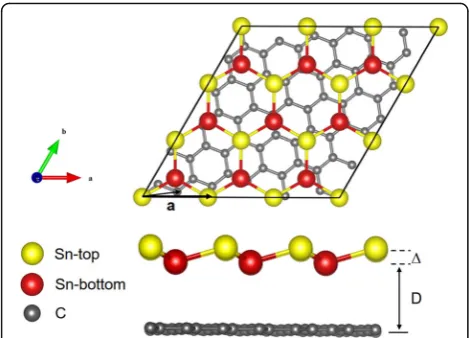
Figure 1 shows the atomic structure of the Sn/G bilayer heterostructure system. The yellow and red atoms repre-sent different types of Sn atoms in the low-buckled mono-layer. A Sn atom in the top layer of stanene is placed on the top of a C atom in graphene. After relaxing, the
buck-ling heightΔis found to be 0.8 Å in this system, and the
interlayer distance from graphene to the bottom Sn layer is 3.5 Å based on the LDA calculation (to be discussed below), indicating that it belongs to the class of vdW type of heterostructures.
LSn/Gin Table 1 is the heterostructure length of the fully
relaxed Sn/G bilayer determined by the LDA, whileLSnand
LG are the lattice constants for the particular unrelaxed
supercells of stanene and graphene, respectively. The lattice
parameter of Sn/G heterostructure is fixed to be (LSn+LG)/
[image:2.595.57.539.614.697.2]2 with a small lattice mismatch for both stanene and
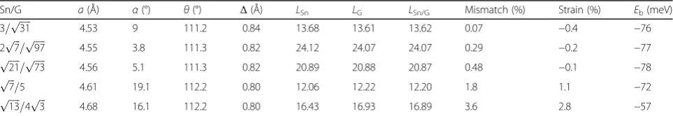
Table 1Heterostructure configurations for the stanene/graphene bilayers (abbreviated as Sn/G)
Sn/G a(Å) α(°) θ(°) Δ(Å) LSn LG LSn/G Mismatch (%) Strain (%) Eb(meV)
3=pffiffiffiffiffi31 4.53 9 111.2 0.84 13.68 13.61 13.62 0.07 −0.4 −76
2pffiffiffi7=pffiffiffiffiffi97 4.55 3.8 111.3 0.82 24.12 24.07 24.07 0.29 −0.2 −77
ffiffiffiffiffi
21
p
=pffiffiffiffiffi73 4.56 5.1 111.3 0.82 20.89 20.88 20.87 0.48 −0.1 −78
ffiffiffi
7
p
=5 4.61 19.1 112.2 0.80 12.06 12.22 12.20 1.8 1.1 −72
ffiffiffiffiffi
13
p
=4pffiffiffi3 4.68 16.1 112.2 0.80 16.43 16.93 16.89 3.6 2.8 −57
Each configuration is built by combining different supercells in individual layers with a relative rotational angleαbetween them.LSn/Gis the lattice constant of the
relaxed bilayer heterostructure and the correspondingais the effective lattice constant of stanene in the relaxed heterostructure, whileLSnandLGare the lattice
graphene. After fully relaxation, it is found thatLSn/Gis very
close toLG, which indicates that there is almost no strain in
graphene layer. The lattice mismatch between the periodic unrelaxed supercell of monolayer stanene and graphene is
defined as mismatch=|LSn−LG|/LG, and it is a quite small
value as shown in Table 1. The strain in the stanene layer is defined by
strain¼ a−a0
a0 ¼
LSn=G−LSn
LSn ; ð1Þ
where a and a0are the relaxed (bilayer) and unrelaxed
primitive lattice constants.
As shown in Table 1, we focus on the heterostructure models that induce a strain of less than 3%. The bond
anglesθand buckling heightΔin stanene will be slightly
affected by the strain as shown in Table 1. In
free-standing monolayer stanene, the bond angle θ is
uni-form, as shown as red circle in Fig. 2. With the presence of a substrate, the bond angles exhibit a small variation of a few degrees, as the lattice symmetry is slight broken
in the Sn layer.θ shown in Table 1 is the average value,
and all the distributions of bond angles are shown in Fig. 2. Obviously, when the strain < 0, the stanene layer is applied by a compressive strain, which causes the
bond angle θ to be slightly smaller and the buckling
height Δ to be higher. There are opposite results when
the strain > 0, the stanene layer is forced by a tensile strain. The change of electronic properties caused by the variation of bond angles will be discussed below.
The vdW interaction between the layers requires spe-cial attention. To quantitatively characterize the inter-layer interaction strength, we define a binding energy
(Eb, per Sn atom) in the Sn/G bilayer as
Eb ¼ESn=G−ESn−EG
NSn ; ð2Þ
whereESn/G,ESn, andEGrepresent the total energies of the
Sn/G heterostructure, corresponding monolayer stanene,
and monolayer graphene, respectively, andNSnis the
num-ber of Sn atoms in this structure. This binding energy for
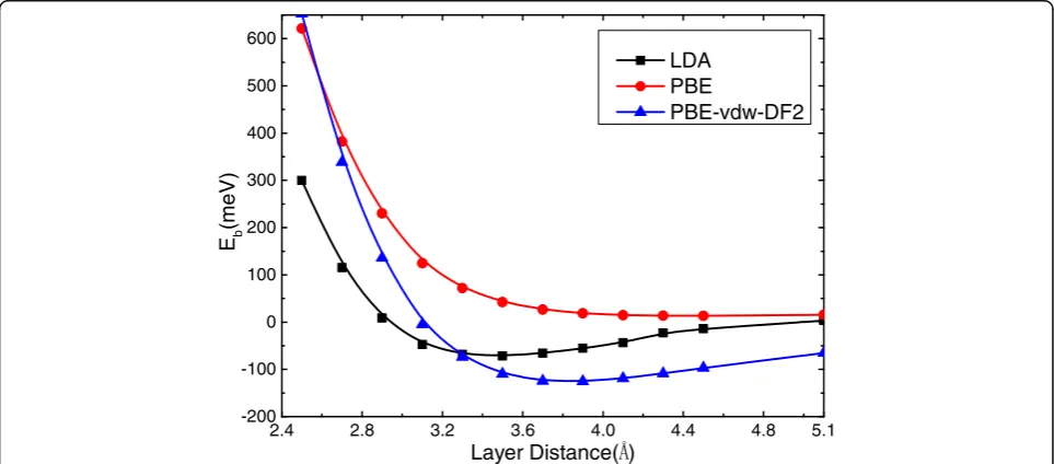
the Snpffiffiffi7=G 5ð Þbilayer is evaluated by various
exchange-correlation functionals, and the results as a function of the layer separation are shown in Fig. 3. Except for the PBE-GGA that fails to create any binding between the layers, other functionals (LDA and PBE-vdW-DF2) predict energy
minima at an interlayer separation around 3.5–3.7 Å. The
LDA gives an energy lowering of 72 meV per Sn atom due to the interlayer interaction, which is higher about 70 meV than the case of explicit PBE vdW calculations, suggesting that the results of PBE vdW method are more credible due to the interlayer interaction. Since we are mostly concerned with relative energies and the electronic structure in the present work, and the variation in the interlayer separation
around 3.5–3.7 Å is not expected to significantly affect the
results. In the following, we will report LDA results at an interlayer separation of 3.5 Å for the simplicity of the
calcu-lations. As shown in Table 1 andEbin Fig. 5b, the smallest
strain structure Snpffiffiffiffiffi21=Gpffiffiffiffiffi73has the lowest binding
energy, which is−78 meV per Sn atom, corresponding the
strongest binding effect. The value is similar to that of
gra-phene/silicene (−66 meV per C atom) within a plane-wave
basis set [40]. It indicates that our calculations forEbwere
reliable. The weak vdW interactions dominate between sta-nene and graphene, suggesting that graphene can be used as an ideal substrate for stanene. Moreover, to verify the
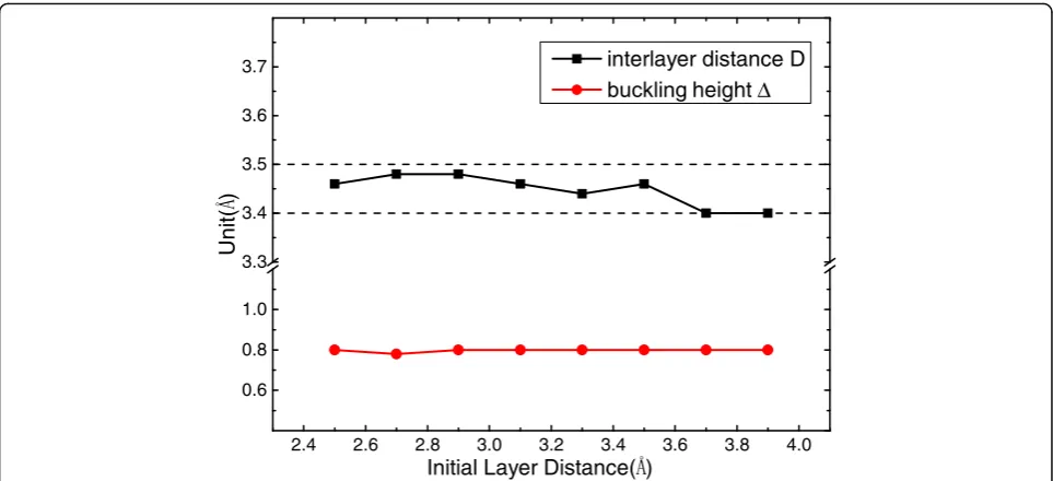
re-liability of the equilibrium interlayer distance D, different
initial layer distance (2.5–3.9 Å) between stanene and
gra-phene has been fully relaxed, getting up to an identical
dis-tance (3.4–3.5 Å) and a uniform buckling heightΔ= 0.8 Å
as shown in Fig. 4.
The energetics of the stanene overlayer can be ad-dressed by examining the energy per Sn atom defined as:
Ec¼ESn=G−EG
NSn −μSn; ð3Þ
where μSn is the chemical potential set to the energy per
atom of bulk Sn. The calculated energies per Sn atom using different heterostructures in Table 1 are plotted as a
func-tion of the strain in Fig. 5a. The value ofEcis positive,
indi-cating that the 2D structure is higher in energy than the 3D diamond structure. Among all the heterostructures we have
considered, Snpffiffiffiffiffi21=Gpffiffiffiffiffi73 has the smallest strain
[image:3.595.56.291.87.256.2](−0.1%) and the lowest energy as expected. The energy dif-ference per atom between different supercell models is smaller than the thermal energy at room temperature (about 26 meV), indicating that multiple phases of different crystalline orientation could coexist at room temperature.
Electronic Structure
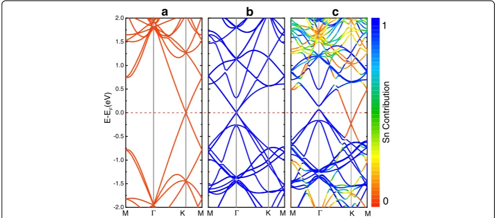
Two-dimensional honeycomb structures exhibit a sym-metry between the sublattices and therefore have a linear energy dispersion in the vicinity of the Dirac points at K point. Figure 6c shows the projected band structures of Sn
3
ð Þ=Gpffiffiffiffiffi31. The relative contribution of stanene is coded by color, in which blue (red) corresponds to the state originating only from stanene (graphene). For com-parison, the energy band structures of the corresponding graphene and isolated stanene monolayer are also show in
Fig. 6a, b. For Sn 3ð Þ=Gpffiffiffiffiffi31, the electronic structure is
not a simple sum of those of each constituent. Forcing on the position of Dirac point reference to the Fermi level, we found a significant change. The Dirac point of stanene
locates at Γshift 0.1 eV above the Fermi level, while
gra-phene moves 0.2 eV below the Fermi level. Meanwhile, it
2.4 2.8 3.2 3.6 4.0 4.4 4.8 5.1 -200
-100 0 100 200 300 400 500 600
Eb
(m
e
V
)
Layer Distance( )
LDA PBE
PBE-vdw-DF2
Fig. 3Interlayer binding energy per Sn atom of the bilayer Snpffiffiffi7=G 5ð Þas a function of interlayer spacing. Results using different exchange-correlation functionals are shown. See text for the geometry and the binding energy definition
-0.5 0.0 0.5 1.0 1.5 2.0 2.5 3.0
110 111 112 113
Sn layer in Sn/G Monolayer Stanene
Angl
e
(
°
)
Strain (%)
[image:4.595.57.540.88.308.2] [image:4.595.57.539.489.701.2]can be seen that, at the Γpoint, theπ and π* bands re-pulse each other, forming a band gap as large as 67 meV. The Fermi level crosses the two Dirac zones of stanene and graphene, inducing weak p-type and n-type doping of them, respectively, and generating a small amount of elec-tron transfer from stanene to graphene. Based on the
lin-ear Dirac-like dispersion relation E(k) = ±ℏνF|k| around
the Fermi levels [55], the charge carrier (hole or electron) concentration of doped graphene can be estimated by the following equation [56, 57]:
Nh=e¼ ðΔEDÞ
2
πℏνFÞ2; ð4Þ
where ΔED is the shift of graphene’s Dirac point (ED)
relative to the Fermi level (EF), that is ΔED=ED−EF.
Our calculated charge carrier concentrations are Nh
(Sn) = 1.4 × 1012 cm−2 and Ne (G) = 1.6 × 1011 cm−2 for
stanene and graphene in bilayer, respectively. These values are larger than the intrinsic charge carrier
con-centration of graphene at room temperature ( n
=πkB2T2/6ℏνF2= 6 × 1010cm−2) [58]. Furthermore, the
charge carrier concentrations of both stanene and gra-phene in Sn/G heterostructure can be tuned via the interfacial spacing [59]. The self-doping phenomenon in Sn/G heterostructure provides an effective and tunable way for new optoelectronic devices.
Figure 7 shows the band structure of other four super-cell models. We can find that the position of the Dirac point located at different high-symmetry point results from the band-folding caused by the various supercell. The graphene substrate introduces an inhomogeneous po-tential that breaks the sublattice symmetry of stanene. For a free-standing stanene monolayer, the bond angles are uniform. For the graphene-supported layer, the bond an-gles have a variation, as shown in Fig. 2; hence, the sublat-tice symmetry is broken, and a gap is opened. And the
opened gaps at the Dirac point for Snpffiffiffi7=G 5ð Þ, Sn 3ð Þ=
Gpffiffiffiffiffi31, Snpffiffiffiffiffi13=G 4 p3ffiffiffi, Snpffiffiffiffiffi21=Gpffiffiffiffiffi73, and Sn 2pffiffiffi7
=Gpffiffiffiffiffi97 are 34, 67, 53, 44, and 22 meV,
respect-ively. The spin–orbit coupling effect is also calculated, and
2.4 2.6 2.8 3.0 3.2 3.4 3.6 3.8 4.0
0.6 0.8 1.0 3.3 3.4 3.5 3.6 3.7
Uni
t(
)
Initial Layer Distance( )
interlayer distance D height Δ
Fig. 4Equilibrium interlayer distanceDof the bilayer Sn(7)/G(5) and buckling heightΔof Sn layer obtained from optimized structure of different initial interlayer distance
[image:5.595.57.539.87.307.2] [image:5.595.56.290.492.683.2]the gap at the Dirac point will reduce after adding the SOC. The results suggest that the gap in the bilayer het-erostructure could be tuned by the interplay between the substrate and SOC effects, moreover by voltage or strain. The characteristics of the Dirac fermions are preserved as shown in Fig. 7b, c accompanied with a small amount of charge transfer from stanene to graphene, as discussed in Sn 3ð Þ=Gpffiffiffiffiffi31.
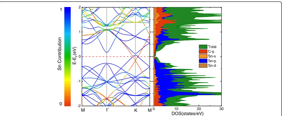
When focusing on Fig. 7a, d, we find that the Dirac points of stanene and graphene are located at the same high-symmetry point K. To investigate the mechanisms of action more clearly, the projected band structure and
density of states (DOS) of Snpffiffiffi7=G 5ð Þ is shown in
Fig. 8. It is clearly seen that there exists a band inversion
around the Fermi level at K point. For stanene, the ori-ginal valence band shifts up to the conduction band, while for graphene, the original conduction band turns into valence band which is below the Fermi level. Mean-while, both the maximum valence band and minimum
conduction band are transformed from the “cone shape”
to the“Mexican-hat shape,”leading to the appearance of
two Dirac feature points with the band gap about 34 meV around the K point. The band inversion associ-ated with the change of band shapes is reminiscent of many topological insulators (TIs) [60, 61]. In order to
ascertain the topological phase transition in the Snpffiffiffi7
=G 5ð Þ heterostructure, we calculate the Z2 topological
invariants. We implement the method proposed by Soluyanov and Vanderbilt [62], in which the 2D Z2
-2.0 -1.5 -1.0 -0.5 0.0 0.5 1.0 1.5 2.0
E-E
F
(e
V)
0.000 0.06667 0.1333 0.2000 0.2667 0.3333 0.4000 0.4667 0.5333 0.6000 0.6667 0.7333 0.8000 0.8667 0.9333 1.000
0 1
S
n
Cont
ri
but
io
n
Fig. 6Electronic structures of theamonolayer graphene,bmonolayer stanene, andcbilayer Sn 3ð Þ=Gpffiffiffiffiffi31. Thered linerepresents the Fermi level, which set to be zero. The relative contribution of stanene is coded by color:blue(red) corresponds to the state originating only from stanene (graphene). The substrate-induced gap is 67 meV for Sn (Γ) and 3 meV for graphene (K)
-2.0 -1.5 -1.0 -0.5 0.0 0.5 1.0 1.5 2.0
Energy(eV)
[image:6.595.55.539.88.301.2] [image:6.595.58.540.528.691.2]invariant is obtained by counting the number of jumps
of the “biggest gap” among the 1D hybrid Wannier
charge centers [63] (WCCs) during the evolution. Although the results have shown that it exhibits a topo-logically trivial phase, it would provide a way and useful guideline for the investigation the QSH insulator and the grown of stanene or other 2D vdW heterostructures.
Conclusions
In conclusion, by first-principle calculations, we found it is possible to synthesize stanene on the graphene sub-strate without destroying its characteristics of the Dirac-fermion-like linear dispersion around Dirac points, due to the weak van der Waals interlayer interaction. In addition, multiple phases of different crystalline orienta-tion of stanene and graphene could coexist at room temperature based on our energetics analysis. Moreover, interlayer interactions in stanene and graphene
hetero-structure can induce tunable band gaps at stanene’s
Di-rac point, and weak p-type and n-type doping of stanene and graphene, respectively, generating a small amount of electron transfer from stanene to graphene. For stanene on graphene, the gap created by the substrate effect is of the same order as that induced by the SOC effect.
Inter-estingly, for model Snpffiffiffi7=G 5ð Þ, there exists a band
in-version around the Dirac zones at K point and emerges a band gap about 34 meV overall the band structure, indicating that it shows a semiconductor feature. Our fundamental study of the structural and electronic prop-erties of these stanene/graphene heterostructures may provide important insight and useful guideline for the grown and applications of stanene or other 2D vdW heterostructures.
Acknowledgements
This work was supported by the National Basic Research Program of China (973 Program) under Grant No. 2014CB643900, the Open Program of State Key Laboratory of Functional Materials for Informatics, the National Natural Science Foundation of China (No. 61675032), the Shanghai Pujiang Program (Grant No. 14PJ1410600), the National Natural Science Foundation for Theoretical Physics Special Fund“Cooperation Program”(No. 11547039), and Shaanxi Institute of Scientific Research Plan projects (No. SLGKYQD2-05).
Authors’Contributions
LYW carried out the calculations. LYW and PFL wrote the manuscript. JYB, CHY, YXS, and SMW helped in the discussions and analysis of the results. PFL and PFG proposed the initial work, supervised the analysis, and revised the manuscript. All authors read and approved the final manuscript.
Competing Interests
The authors declare that they have no competing interests.
Author details 1
State Key Laboratory of Information Photonics and Optical Communications, Ministry of Education, Beijing University of Posts and Telecommunications, P.O. Box 72, Beijing 100876, China.2School of Physics and
Telecommunication Engineering, Shanxi University of Technology (SNUT), Hanzhong 723001, Shaanxi, China.3Beijing Computational Science Research Center, Beijing 100084, China.4State Key Laboratory of Functional Materials for Informatics, Shanghai Institute of Microsystem and Information Technology, Chinese Academy of Sciences, Shanghai 200050, China. 5
Photonics Laboratory, Department of Microtechnology and Nanoscience, Chalmers University of Technology, 41296 Gothenburg, Sweden.
Received: 3 August 2016 Accepted: 9 November 2016
References
1. Novoselov KS, Geim AK, Morozov SV, Jiang D, Zhang Y, Dubonos SV, Firsov AA et al (2004) Electric field effect in atomically thin carbon films. Science 306:666–669
2. Geim AK, Novoselov KS (2007) The rise of graphene. Nat Mater 6:183–191 3. Zhang S, Zhou J, Wang Q, Chen X, Kawazoe Y, Jena P (2015)
Penta-graphene: a new carbon allotrope. Proc Natl Acad Sci 112(8):2372–2377 4. Wang FQ, Yu J, Wang Q, Kawazoe Y, Jena P (2016) Lattice thermal
conductivity of penta-graphene. Carbon 105:424–429 -2
-1 0 1 2
1
Sn
C
o
ntr
ibution
E-EF
(e
V
)
0
Total C-p Sn-s Sn-p Sn-d
[image:7.595.59.539.86.284.2]5. Li X, Zhang S, Wang FQ, Guo Y, Liu J, Wang Q (2016) Tuning the electronic and mechanical properties of penta-graphene via hydrogenation and fluorination. Phys Chem Chem Phys 18(21):14191–14197
6. Zhang S, Zhou J, Wang Q, Jena P (2016) Beyond graphitic carbon nitride: nitrogen-rich penta-CN2 sheet. J Phys Chem C 120(7):3993–3998 7. Cahangirov S, Topsakal M, Aktürk E,Şahin H, Ciraci S (2009) Two-and
one-dimensional honeycomb structures of silicon and germanium. Phys Rev Lett 102:236804
8. Liu H, Gao J, Zhao J (2013) Silicene on substrates: a way to preserve or tune its electronic properties. J Phys Chem C 117(20):10353–10359
9. Gao J, Zhao J (2012) Initial geometries, interaction mechanism and high stability of silicene on Ag (111) surface. Sci Rep 2:861
10. Resta A, Leoni T, Barth C, Ranguis A, Becker C, Bruhn T, Le Lay G et al (2013) Atomic structures of silicene layers grown on Ag (111): scanning tunneling microscopy and noncontact atomic force microscopy observations. Sci Rep 3:2399
11. Guo Y, Zhang S, Zhao T, Wang Q (2016) Thermal exfoliation of stoichiometric single-layer silica from the stishovite phase: insight from first-principles calculations. Nanoscale 8(20):10598–10606
12. Kaloni TP, Singh N, Schwingenschlögl U (2014) Prediction of a quantum anomalous Hall state in Co-decorated silicene. Physical Review B 89:035409 13. Ju W, Li T, Su X, Cui H, Li H (2016) Engineering magnetism and electronic
properties of silicene by changing adsorption coverage. Appl Surf Sci 384:65–72 14. Dávila ME, Xian L, Cahangirov S, Rubio A, Le Lay, G (2014). Germanene: a
novel two-dimensional germanium allotrope akin to graphene and silicene. New J Phys 16(9):095002
15. Li L, Lu SZ, Pan J, Qin Z, Wang YQ, Wang Y et al (2014) Buckled germanene formation on Pt (111). Adv Mater 26(28):4820–4824
16. Singh N, Schwingenschlögl U (2014) Topological phases of silicene and germanene in an external magnetic field: quantitative results. Physica status solidi (RRL)-Rapid Research Letters 8(4):353–356
17. Watanabe K, Taniguchi T, Kanda H (2004) Direct-bandgap properties and evidence for ultraviolet lasing of hexagonal boron nitride single crystal. Nat Mater 3(6):404–409
18. Song L, Ci L, Lu H, Sorokin PB, Jin C, Ni J et al (2010) Large scale growth and characterization of atomic hexagonal boron nitride layers. Nano Lett 10(8):3209–3215
19. Hong J, Hu Z, Probert M, Li K, Lv D, Yang X et al (2015) Exploring atomic defects in molybdenum disulphide monolayers. Nature communications 6:6293 20. He H, Lu P, Wu L, Zhang C, Song Y, Guan P, Wang S (2016) Structural
properties and phase transition of Na adsorption on monolayer MoS2. Nanoscale Res Lett 11(1):1–8
21. Cai Y, Chu CP, Wei CM, Chou MY (2013) Stability and electronic properties of two-dimensional silicene and germanene on graphene. Physical Review B 88(24):245408
22. Liu B, Baimova JA, Reddy CD, Dmitriev SV, Law WK, Feng XQ, Zhou K (2014) Interface thermal conductance and rectification in hybrid graphene/silicene monolayer. Carbon 79:236–244
23. Roth S, Matsui F, Greber T, Osterwalder J (2013) Chemical vapor deposition and characterization of aligned and incommensurate graphene/hexagonal boron nitride heterostack on Cu (111). Nano Lett 13(6):2668–2675
24. Yang W, Chen G, Shi Z, Liu CC, Zhang L, Xie G et al (2013) Epitaxial growth of single-domain graphene on hexagonal boron nitride. Nat Mater 12(9): 792–797
25. Kaloni TP, Gangopadhyay S, Singh N, Jones B, Schwingenschlögl U (2013) Electronic properties of Mn-decorated silicene on hexagonal boron nitride. Physical Review B 88(23):235418
26. Ding Y, Wang Y (2013) Electronic structures of silicene/GaS heterosheets. Appl Phys Lett 103(4):043114
27. Feng JW, Liu YJ, Wang HX, Zhao JX, Cai QH, Wang XZ (2014) Gas adsorption on silicene: a theoretical study. Comput Mater Sci 87:218–226
28. Roy K, Padmanabhan M, Goswami S, Sai TP, Ramalingam G, Raghavan S, Ghosh A (2013) Graphene-MoS2 hybrid structures for multifunctional photoresponsive memory devices. Nat Nanotechnol 8(11):826–830 29. Zhang W, Chuu CP, Huang JK, Chen CH, Tsai ML, Chang YH et al (2014)
Ultrahigh-gain photodetectors based on atomically thin graphene-MoS2 heterostructures. Scientific reports 4(7484):3826–3826
30. Bernardi M, Palummo M, Grossman JC (2013) Extraordinary sunlight absorption and one nanometer thick photovoltaics using two-dimensional monolayer materials. Nano Lett 13(8):3664–3670
31. Yu Y, Hu S, Su L, Huang L, Liu Y, Jin Z, Purezky AA, Geohegan DB, Kim KW, Zhang Y, Cao L et al (2014) Equally efficient interlayer exciton relaxation and improved absorption in epitaxial and nonepitaxial MoS2/WS2
heterostructures. Nano Lett 15(1):486–491
32. Liu H, Neal AT, Zhu Z, Luo Z, Xu X, Tománek D, Ye PD (2014) Phosphorene: an unexplored 2D semiconductor with a high hole mobility. ACS Nano 8(4):4033–4041
33. Padilha JE, Fazzio A, da Silva AJ (2015) van der Waals heterostructure of phosphorene and graphene: tuning the Schottky barrier and doping by electrostatic gating. Phys Rev Lett 114(6):066803
34. Liu CC, Jiang H, Yao Y (2011) Low-energy effective Hamiltonian involving spin-orbit coupling in silicene and two-dimensional germanium and tin. Physical Review B 84(19):195430
35. Xu Y, Yan B, Zhang HJ, Wang J, Xu G, Tang P, Zhang SC et al (2013) Large-gap quantum spin Hall insulators in tin films. Phys Rev Lett 111(13):136804 36. Fang Y, Huang ZQ, Hsu CH, Li X, Xu Y, Zhou Y et al (2015) Quantum spin
Hall states in stanene/Ge (111). Scientific reports 5:14196
37. Zhang GF, Li Y, Wu C (2014) Honeycomb lattice with multiorbital structure: topological and quantum anomalous Hall insulators with large gaps. Physical Review B 90(7):075114
38. Gao J, Zhang G, Zhang YW (2016) Exploring Ag (111) substrate for epitaxially growing monolayer stanene: a first-principles study. Sci Rep 6:29107 39. Zhou H, Cai Y, Zhang G, Zhang YW (2016) Quantum thermal transport in
stanene. Physical Review B 94(4):045423
40. Zhang RW, Ji WX, Zhang CW, Li P, Wang PJ (2016) Prediction of flatness-driven quantum spin Hall effect in functionalized germanene and stanene. Phys Chem Chem Phys 18(40):28134–28139
41. Xu Y, Gan Z, Zhang SC (2014) Enhanced thermoelectric performance and anomalous Seebeck effects in topological insulators. Phys Rev Lett 112(22): 226801
42. Wang J, Xu Y, Zhang SC (2014) Two-dimensional time-reversal-invariant topological superconductivity in a doped quantum spin-Hall insulator. Physical Review B 90(5):054503
43. Wu SC, Shan G, Yan B (2014) Prediction of near-room-temperature quantum anomalous Hall effect on honeycomb materials. Phys Rev Lett 113(25): 256401
44. Zhu FF, Chen WJ, Xu Y, Gao CL, Guan DD, Liu CH, Jia JF et al (2015). Epitaxial growth of two-dimensional stanene. Nat Mater 14(10):1020-1025
45. Kohn W, Sham LJ (1965) Self-consistent equations including exchange and correlation effects. Phys Rev 140(4A):A1133
46. Kresse G, Furthmüller J (1996) Efficiency of ab-initio total energy calculations for metals and semiconductors using a plane-wave basis set. Comput Mater Sci 6(1):15–50
47. Blöchl PE (1994) Projector augmented-wave method. Physical Review B 50(24):17953
48. Kresse G, Joubert D (1999) From ultrasoft pseudopotentials to the projector augmented-wave method. Physical Review B 59(3):1758
49. Ceperley DM, Alder BJ (1980) Ground state of the electron gas by a stochastic method. Phys Rev Lett 45(7):566
50. Perdew JP, Burke K, Ernzerhof M (1996) Generalized gradient approximation made simple. Phys Rev Lett 77(18):3865
51. Grimme S (2006) Semiempirical GGA‐type density functional constructed with a long‐range dispersion correction. J Comput Chem 27(15):1787–1799 52. Monkhorst HJ, Pack JD (1976) Special points for Brillouin-zone integrations.
Physical review B 13(12):5188
53. Riedl C, Coletti C, Starke U (2010) Structural and electronic properties of epitaxial graphene on SiC (0 0 0 1): a review of growth, characterization, transfer doping and hydrogen intercalation. J Phys D Appl Phys 43(37):374009 54. Wang D, Chen L, Wang X, Cui G, Zhang P (2015) The effect of substrate and
external strain on electronic structures of stanene film. Phys Chem Chem Phys 17(40):26979–26987
55. Neto AC, Guinea F, Peres NM, Novoselov KS, Geim AK (2009) The electronic properties of graphene. Rev Mod Phys 81(1):109
56. Wang Y, Ni Z, Liu Q, Quhe R, Zheng J, Ye M et al (2015) All-metallic vertical transistors based on stacked Dirac materials. Adv Funct Mater 25(1):68–77 57. Qin R, Wang CH, Zhu W, Zhang Y (2012) First-principles calculations of
mechanical and electronic properties of silicene under strain. Aip Advances 2(2):022159
59. Hu W, Yang J (2016) First-principles study of two-dimensional van der Waals heterojunctions. Comput Mater Sci 112:518–526
60. Du A, Ng YH, Bell NJ, Zhu Z, Amal R, Smith SC (2011) Hybrid graphene/ titania nanocomposite: interface charge transfer, hole doping, and sensitization for visible light response. J Phys Chem Letters 2(8):894–899 61. Ristein J, Mammadov S, Seyller T (2012) Origin of doping in
quasi-free-standing graphene on silicon carbide. Phys Rev Lett 108(24):246104 62. Soluyanov AA, Vanderbilt D (2011) Computing topological invariants
without inversion symmetry. Physical Review B 83(23):235401 63. Marzari N, Vanderbilt D (1997) Maximally localized generalized Wannier
functions for composite energy bands. Physical review B 56(20):12847
Submit your manuscript to a
journal and benefi t from:
7Convenient online submission
7Rigorous peer review
7Immediate publication on acceptance
7Open access: articles freely available online
7High visibility within the fi eld
7Retaining the copyright to your article